quantum wells
DISSERTATION
zur Erlangung des akademischen Grades doctor rerum naturalium
(Dr. rer. nat.) im Fach Physik eingereicht an der
Mathematisch-Naturwissenschaftlichen Fakultät I Humboldt-Universität zu Berlin
von
Herr M.Sc.-Phys. Odilon D. D. Couto Jr.
geboren am 30.11.1979 in Guaxupé/Brasilien
Präsident der Humboldt-Universität zu Berlin:
Prof. Dr. h.c. Christoph Markschies
Dekan der Mathematisch-Naturwissenschaftlichen Fakultät I:
Prof. Dr. Lutz-Helmut Schön Gutachter:
1. Prof. Dr. K. H. Ploog 2. Prof. Dr. O. Benson 3. Prof. Dr. F. Iikawa
eingereicht am: 26. Mai 2008
Tag der mündlichen Prüfung: 29. September 2008
manipulate optically generated spin ensembles in (110) GaAs quantum wells (QWs). The strong carrier confinement into the SAW piezoelectric potential allows for the transport of spin-polarized carrier packets along well-defined channels with the propagation velocity of the acoustic wave. In this way, spin transport over distances exceeding 60 µm is achieved, corresponding to spin lifetimes longer than 20 ns. The demonstration of such extremely long spin lifetimes is enabled by three main factors: (i) Suppression of the D’yakonov-Perel’ spin relaxation mechanism for z-oriented spins in (110) III- V QWs; (ii) Suppression of the Bir-Aronov-Pikus spin relaxation mechanism caused by the type-II SAW piezoelectric potential; (iii) Suppression of spin relaxation induced by the mesoscopic carrier confinement into narrow stripes along the SAW wave front direction.
A spin transport anisotropy under external magnetic fields (Bext) is demonstrated for the first time. Employing the well-defined average carrier momentum impinged by the SAW, we analyze the spin dephasing dynamics during transport along the [001] and[1¯10]in-plane directions. For transport along [001], fluctuations of the internal magnetic field (Bint), which arises from the spin-orbit interaction associated with the bulk inversion asymme- try of the crystal, lead to decoherence within 2 ns as the spins precess around Bext. In contrast, for transport along the[1¯10]direction, the z-component of the spin polarization is maintained for times one order of magnitude longer due to the non-zero average value of Bint. The dephasing anisotropy be- tween the two directions is fully understood in terms of the dependence of the spin-orbit coupling on carrier momentum direction, as predicted by the D’yakonov-Perel’ mechanism for the (110) system.
semiconductor, spin transport, (110) GaAs quantum wells, surface acoustic waves
Im Mittelpunkt dieser Arbeit stehen der Transport und die Manipulation optisch angeregter Elektronen-Spins in (110) Quantenfilmen (quantum wells, QWs) mittels akustischer Oberflächenwellen (surface acoustic waves, SAWs).
Der starke räumliche Einschluss der Ladungsträger im akustisch erzeugten Potenzial erlaubt spinerhaltenden Ladungsträgertransport mit der akusti- schen Geschwindigkeit. Auf diese Weise wird langreichweitiger Spintransport über Distanzen > 60 µm demonstriert, welche Spinlebenszeiten von mehr als 20 ns entsprechen. Erreicht werden diese extrem langen Spinlebenszei- ten durch drei Effekte: (i) Der D’yakonov-Perel’-Mechanismus ist für Spins in Wachstumsrichtung von (110)-QWs in III-V-Halbleitern unterdrückt. (ii) Aufgrund des Typ-II piezoelektrischen Potenzials der akustischen Oberflä- chenwelle ist der Bir-Aronov-Pikus Spinrelaxations-Mechanismus sehr schwach.
(iii) Der starke Einschluss der Ladungsträger in mesoskopische Bereiche sta- bilisiert den Spin zusätzlich.
In der vorliegenden Arbeit wird erstmals eine Anisotropie des Spintrans- ports in einem externen Magnetfeld (Bext) nachgewiesen. Hierzu wurde die elektronische Spindynamik während des akustischen Transports entlang der [001]- bzw.[1¯10]-Richtung untersucht. Während des Transports entlang der [001]-Richtung führt die Präzession der Elektronenspins um das fluktuie- rende interne Magnetfeld (Bint), das vom Fehlen eines Inversionszentrums im GaAs-Kristallgitter herrührt, zu Spinkohärenzzeiten von etwa 2 ns. Im Gegensatz hierzu ist beim Transport entlang der [1¯10]-Richtung die Spin- relaxation für Spins in Wachstumsrichtung um eine Größenordnung langsa- mer. Grund hierfür ist die endliche mittlere Größe des internen effektiven Magnetfeldes Bint für Transport entlang dieser Richtung. Die beobachtete Anisotropie in der Spindynamik für die beiden Transportrichtungen wird vollständig im Rahmen der Spin-Bahn-Kopplung und des D’yakonov-Perel’- Mechanismus beschrieben und quantitativ erklärt.
Halbleiter, Elektronenspinrelaxation, (110) Quantenfilmen, akustischer Oberflächenwellen
Contents
List of Figures xi
List of Tables xvii
1 Introduction 1
1.1 Spintronics . . . 1
1.2 Acoustically induced transport . . . 3
1.3 (110) quantum wells . . . 5
1.4 This work . . . 5
2 Surface acoustic wave on GaAs (110) surfaces 9 2.1 Surface acoustic wave dynamics . . . 9
2.1.1 Mathematical description . . . 10
2.1.2 Abbreviated notation . . . 11
2.2 SAW propagation on (110) GaAs surfaces . . . 14
2.2.1 Numerical calculation of the SAW eigenmodes . . . 14
2.2.2 Propagation along the [001] direction . . . 18
2.2.3 Propagation along the[1¯10] direction . . . 19
2.3 Band structure modulation by SAWs . . . 19
2.3.1 Strain field . . . 19
2.3.2 Piezoelectric field . . . 22
3 Spin relaxation in (110) GaAs quantum wells 29 3.1 Introduction . . . 29
3.2 Spin-orbit interaction . . . 30
3.2.1 Spin-splitting in quasi-2D zinc-blende semiconductors 31 3.2.2 Sources of inversion asymmetry . . . 33
3.2.3 Selection rules and optical orientation . . . 34
3.3.1 D’yakonov-Perel’ mechanism . . . 38
3.3.2 Bir-Aronov-Pikus mechanism . . . 41
3.4 Spin dephasing under external magnetic fields . . . 42
3.4.1 Spin dephasing during transport along the [001] direction 43 3.4.2 Spin dephasing during transport along the[1¯10]direction 46 3.5 SAW induced spin relaxation . . . 48
3.5.1 Bychkov-Rashba mechanism . . . 48
3.5.2 The influence of strain on spin relaxation . . . 50
3.6 Discussion . . . 52
4 Experimental details 57 4.1 Sample preparation . . . 57
4.1.1 MBE growth of (110)-oriented structures . . . 57
4.1.2 (110) GaAs quantum wells for acoustic transport . . . 59
4.1.3 ZnO sputtering . . . 62
4.2 SAW generation . . . 63
4.3 Optical experiments under surface acoustic wave . . . 68
5 Acoustically induced spin transport 73 5.1 Acoustic carrier transport . . . 74
5.1.1 The role of the ZnO layer for carrier transport . . . . 75
5.1.2 Transport efficiency . . . 76
5.1.3 Band gap modulation . . . 77
5.2 Acoustic spin transport . . . 82
5.2.1 The role of the ZnO layer for spin transport . . . 82
5.3 Spin relaxation during acoustic transport . . . 84
5.3.1 Light intensity . . . 85
5.3.2 Temperature . . . 86
5.3.3 Acoustic power . . . 87
6 Spin manipulation during acoustic transport 96 6.1 Coherent spin transport . . . 97
6.1.1 Spin relaxation along the [001] direction . . . 97
6.1.2 Spin relaxation along the [1¯10] direction . . . 99
6.2 Spin transport anisotropy . . . 100
6.2.2 Spin dephasing along the[1¯10]direction . . . 105
7 Conclusions 109
Bibliography 113
A Parameters 127
A.1 Fundamental constants . . . 127 A.2 Material parameters for GaAs . . . 128
Abbreviations 129
Acknowledgements 130
Selbständigkeitserklärung 132
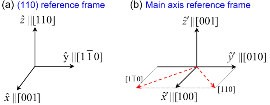
2.1 (a) Rotated reference frame oriented along the main axes of the (110) zinc blende surface. (b) Conventional reference sys- tem for GaAs/AlGaAs cubic crystal structures. . . 16 2.2 Linear dispersion calculated for the surface acoustic modes
along the xˆ k [001] andyˆk [1¯10] directions of the (110) QW structure described in Table 2.1 . . . 18 2.3 (a) Characteristic particle displacements fields ux and uz of
a Rayleigh SAW. (b) Profiles for the vertical displacementuz along the z direction for the Rayleigh wave propagating along the [001] direction of the (110) oriented multilayer structure depicted in Table 2.1. The calculation was performed forλSAW
= 5.6µm andPl = 200 W/m. . . 19 2.4 (a) Particle displacement fielduxfor a Bleustein-Gulyaev SAW
propagating along the [1¯10] direction of the (110) GaAs sur- face. (b) Calculated depth dependence ofuxwithPl= 200 W/m for the multilayer structure presented in Table 2.1. . . 20 2.5 Carrier transport mechanism: the SAW piezoelectric field in-
duces a moving type-II potential modulation, spatially sepa- rating the optically generated carriers (electrons are denoted by ’-’ and holes by ’+’). ¯hωcorresponds to the photon energy used to excite the electron to the CB. . . 22 2.6 Calculated depth profiles for the piezoelectric potential ampli-
tudeφsaw for the acoustic modes propagating along the [001]
and [1¯10] directions for the multilayer structure presented in Table 2.1 (a) without ZnO and (b) with the 500 nm thick ZnO film on top. . . 24
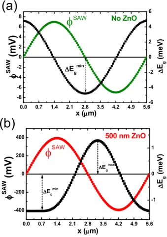
for propagation along the [001] (filled dots) and[1¯10](squares) directions for the structure presented in Table 2.1. The same calculations performed without ZnO are presented by opened circles, where the modulation amplitude of Ez is multiplied by a factor of 10 (opened dots) for better visualization. . . 25 2.8 Calculated piezoelectric potential amplitude and bandgap mod-
ulation (a) in the absence and (b) presence of a 500 nm-thick ZnO layer. The relative phase between φsaw and ∆Eg de- termines the occupation of carriers along one cycle of the Rayleigh SAW propagating along the [001] direction. For the calculations,Pl = 200 W/m. . . 26 3.1 Energy splitting of the conduction (CB) and the valence (VB)
bands of a quasi-2D semiconductor system when the SO-interaction is present. ∆ESOis the energy splitting of the CB, which gives rise to a carrier momentum-dependent internal magnetic field BSO(k). . . 32 3.2 Optical selection rules at theΓ-point for 3D and 2D semicon-
ductor systems. Due to the SO coupling, incident left circu- larly polarized light σ− excites electrons with spin 1/2 with 3 times higher probability than -1/2 into the CB. The same rules hold for the recombination of the excited carriers to the ground state. . . 35 3.3 Internal magnetic field configuration in (110) QWs. Bintpoints
always along the growth direction, preserving thez-componentˆ of the electron spin and avoiding fast spin relaxation. . . 41 3.4 Vector scheme illustrating the longitudinal (s`) and the trans-
verse (st) spin polarization components (with respect toBR) for spin transport along the[1¯10]direction. . . 47 3.5 Effective magnetic field in the QW plane introduced by the
SIA contribution to the SO-coupling. The internal Bychkov- Rashba fieldBbr lies in the QW plane and points always per- pendicularly to the carrier momentum direction. . . 49
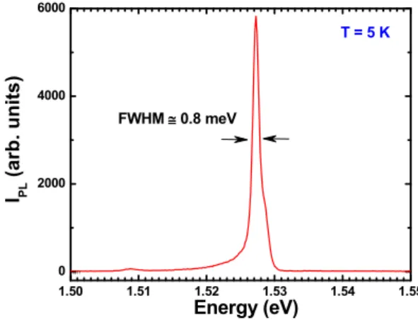
[1¯10] directions. . . 53 4.1 PL emission of the 18 nm-thick GaAs QW structure of Ta-
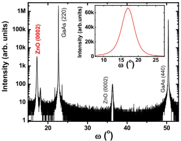
ble 4.1. The small FWHM of 0.8 meV reflects the high degree of structural perfection. . . 61 4.2 X-ray diffraction curve of sample A after the ZnO sputtering
(cf. Table 4.1). The ZnO (0002) diffraction peak from the ZnO crystallites with c-axis orientation perpendicular to the film surface is detected at ω = 17.23◦. The inset shows a rocking curve taken around this peak. . . 63 4.3 (a) Configuration of the IDTs on top of a (110) GaAs QW
sample with (Al,Ga)As barriers. The sample is coated with a piezoelectric ZnO film. IDTs were designed to launch SAW beams along the [001] and[1¯10]surface directions. (b) Finger shape of a focusing IDT, defining the angular apertureφand focusing distancer0 of the acoustic beam. . . 64 4.4 Sample surface image after the processing procedure. The
dark area corresponds to the ZnO film, on top of which four metal IDTs (Al) are deposited. The focusing acoustic beams are generated by the IDTs fingers indicated by arrows. . . 66 4.5 rf-reflection coefficient s11 measurements on IDTs along the
[001] and [1¯10] for sample A, (a) and (b), respectively; the corresponding curves for sample B are shown in (c) and (d). . 67 4.6 Experimental setup for the optical studies: a linearly polarized
laser pulse becomes right circularly polarized after passing a λ/4 plate; an objective focuses the beam on the SAW path to generate spin polarized carriers; the emitter PL is collected by the same objective. Before entering the monochromator, the right (IR) and left (IL) circularly polarized PL compo- nents are separated by a polarization displacement prism and simultaneously detected in different areas of a CCD camera. . 69
optically generated at a spot G and transported by the SAW, which creates a lateral confinement potential with periodicity given by λSAW. The PL emitted along the path gives the degree of spin polarization of the electrons. . . 74 5.2 PL images of the acoustic transport in (a) Sample B, (b)
Sample A, which was ZnO-coated. The transport takes place within the 18 nm-thick GaAs QWs in both structures [cf. Ta- bles 4.1 and 4.2]. Note the difference in magnitude between the horizontal axes in both pictures. . . 75 5.3 PL intensity (IPL) integrated across the SAW beam recorded
for sample A under different acoustic powersPrf. IPL reduces as the acoustic power increases, demonstrating the quenching ofe-hh recombination at the generation spot G and the sub- sequent carrier transport. The squares (right vertical axis) present the PL intensity in the absence of the SAW [IPL(no SAW)]. . . 77 5.4 PL spectra as a function of SAW power for sample B. The
inset corresponds to a zoom in the emission line of the GaAs substrate, showing the band splitting caused by the penetra- tion of the SAW strain field. . . 78 5.5 Experimental PL line splitting ∆E (filled squares) as a func-
tion of the effective acoustic power for sample B. The calcu- lated values for∆Eg taking into account the modulation due to the SAW strain field are shown by empty squares. . . 79 5.6 PL spectra as a function of SAW power sample A, which has
a 500 nm-thick ZnO layer on top. . . 80 5.7 Experimental∆Egmin (filled squares) as a function of the ef-
fective acoustic power for sample A. The calculated values of
∆Egmin taking into account only the modulation due to the strain field (empty squares) and strain plus the piezoelectric- field-induced QCSE (circles) are also shown. . . 81 5.8 PL profiles of the rightIRand leftILcircularly polarized light
demonstrating a net spin transport along the SAW channel in (a) sample B (without ZnO) and (b) sample A (ZnO-coated).
The solid lines show the PL profiles in the absence of a SAW. 83
ple A (circles), respectively. The solid lines correspond to exponential fits. . . 85 5.10 Dependence of spin polarization during transport on light ex-
citation powerPex for sample A, recorded at T = 15 K and using Prf = 10 dBm. The solid lines are exponential decay fits to the data. . . 86 5.11 Spin depolarization along the transport channel recorded at
different temperatures usingPrf = 9 dBm and Pex = 4µW. . 87 5.12 Normalized PL intensity emitted along the transport channel
for different effective acoustic powersPSAW, recorded at 15 K. 88 5.13 (a) Dependence of the spin relaxation time (left) and spin
transport length (right) on the effective acoustic power for sample A. The lifetimes were obtained from the relationτz = Ls/vx, with vx = 2930 m/s. (b) Spin polarization profiles for different acoustic power obtained for sample B. . . 89 5.14 Illustration of the spin scattering in the SAW potential (φsaw):
(a) An electron crosses the confinement direction and scat- ters at the potential boundary. IfλSO >> xc, the precession around BSO is small and the spin orientation is expected to be preserved. (b) WhenλSO < xc, spin memory is lost after scattering. . . 91 5.15 (a) Larmor precession frequencies ΩRs and ΩRbr induced by
the SAW strain and piezoelectric fields, respectively, over one SAW cycle. On the right vertical axis, the amplitude of the SAW piezoelectric field is displayed. (b) Calculated effective magnetic field induced by the SIA like contribution of the SAW fields to spin relaxation, analyzed at the minimum of the electronic energy (−eφsaw) in (a). . . 94 6.1 (a) Stroboscopic images showing thee-hh PL emitted during
acoustic transport along the [001] direction at∆t= 0.2, 4.2, 8.2, and 12.2 ns. (b) PL intensity with right IR (filled dot profiles) and leftIL (empty dot profiles) circular polarization measured for the delays∆t shown in (a). . . 98
for transport along the [001] direction. The dashed line is an exponential fit. (b) Mean position of the PL (xc) emitted by the transported carriers as a function of∆t. The linear fit pro- vides the spin transport velocity along the SAW propagation direction. . . 99 6.3 (a) Spin polarization decay as a function of time delay (∆t)
relative to the excitation pulse for transport along the [1¯10]
direction. The dashed line is an exponential fit. (b) Mean packet position (yc) as a function of∆t, from which we obtain the spin transport velocity along this direction. . . 100 6.4 Spin polarization ρz during transport along xˆ under differ-
ent external magnetic fields Bext applied along y. The topˆ horizontal axis shows the spatial coordinates (x =vx∆t) cor- responding to the delays∆t on the bottom axis. The dashed and solid lines are fits to exponential decay and to the spin dephasing model, respectively. . . 102 6.5 (a) Spatial dependence of the spin polarization decay under
different external magnetic fields obtained in CW measure- ments. (b) Average value of ρ¯z as a function of the applied fieldBext. . . 104 6.6 Spin polarizationρzduring transport alongyˆk[1¯10]under ex-
ternal magnetic field. The dashed and solid lines are fittings to an exponential decay and to the spin dephasing model, re- spectively. The inset shows a vector scheme illustrating the longitudinal (s`) and transverse (st) spin polarization compo- nents relative to the direction of the resultant fieldBR. . . 106 6.7 Magnetic field dependence ofρz measured at fixed delays ∆t
during transport along xˆ (circles) and yˆ (dots and squares).
The dashed and solid lines are fittings to the dephasing models for motion alongxˆ andy, respectively. . . 107ˆ
2.1 (110)-oriented multilayer structure used in the calculation of the SAW propagation modes containing a 18 nm wide GaAs QW with Al0.3Ga0.7As barriers. The ZnO film was deposited on the III-V surface after MBE growth. . . 17 4.1 Layer structure of sample A consisting of a 18 nm-thick GaAs
QW with Al0.3Ga0.7As barriers. . . 60 4.2 Layer structure of sample B consisting of a 18 nm-thick GaAs
QW with Al0.3Ga0.7As barriers. . . 62
Introduction
This introductory chapter describes our motivation to study spin transport phenomena using surface acoustic waves (SAWs) in (110) GaAs quantum wells (QWs). We start with a brief introduction to spintronics, a broad and intensive research field devoted to the understanding and control of the spin degree of freedom in solid-state systems. In the following, we show that SAWs provide a powerful tool for transport and manipulation of carriers, as well as spins, in a variety of physical systems. In the last two sections, we comment on the special characteristics of III-V QWs oriented along the [110]
direction for spin transport and, in particular, the advantages of employing them for acoustic transport. Besides basic physics interests, controllable spin transport in (110) QWs has the potential for future applications in devices based on SAW-induced spin transport.
1.1 Spintronics
The goal of spintronics is to understand the interaction between the particle spin and its environment, mostly aiming at the application of the acquired knowledge in useful devices. Fundamental studies on spintronics include in- vestigations of spin generation, injection, transport, and manipulation. The fact that spintronics offers an opportunity for combining standard microelec- tronics with spin-dependent effects has recently lead to an increasing interest to this field [10, 11, 145, 151].
Some of the potential advantages of spin-based devices in comparison to charge-based ones include higher operation speeds and lower switching
energies. In charge-based devices the speed is limited by the capacitance of the device and the drive current. In the case of semiconductor spintronics, the device operation relies on coherent processes, the speed limitations are given by the typical precession frequencies of the electron spins, which, in general, range from GHz to THz. For example, in order to rotate a spin by 180◦ at THz frequencies, an energy splitting of the order of 4 meV must be generated between the up and down spins. This energy is approximately an order of magnitude lower than the thermal energy at room temperature.
The small energy differences between spin levels is, nevertheless, a benefit and a challenge for semiconductor spintronics. Thermal equilibrium cannot be relied on to keep the information ’safe’, and the development of room temperature operating devices is one of the main challenges.
New ways of information processing can also be implemented using spin- tronics. Spin-based solid-state approaches for quantum computation provide the potential for fixing isolated quantum degrees of freedom in space, by em- bedding quantum dots or ions within a solid matrix, and then address those degrees of freedom optically or with small electrical contacts. This is a highly successful field of spin manipulation in semiconductors for solid-state quan- tum computation. For a review, see Ref. [70]. The two-level spin system has also called attention for its potential application on quantum communica- tion [11]. The preparation of entangled pairs of qubits and the transmission of information via quantum states has focused efforts on issues like spin transport and coherence for information transmission [44]. Security of in- formation exchange is also enhanced in such cases. Promising proposals for quantum key distribution schemes rely, in general, on the important security features provided by quantum cryptography [18]. In most of the approaches proposed for the quantum computation, communication and information se- curity, a very small number of particles is considered. In this work, however, we focus on ensembles of spins.
Spintronic device manufacturing was boosted by the discovery of the gi- ant magnetoresistance (GMR) [12, 19], the huge variation of electrical resis- tance with the magnetization. GMR enabled the development of information storage technologies based on metallic spintronic devices, such as read heads for hard disks and magnetic random access memories (MRAM). Informa- tion processing using the spin degree of freedom (not necessarily restricting the number of particles) has received considerable attention since the pro-
posal of an electronic analog of the electro-optic modulator1 by Datta and Das [40]. Maybe, the discovery of GMR and the Datta and Das proposal, can be considered the two spintronics headstones2. After them, a search for materials with intrinsic high spin polarization and/or interesting properties for applications employing spin phenomena has been witnessed. Recently, the employment of thin ferromagnetic films for injection and detection of spin polarized electrons in a Si transport channel lead to the demonstration of the first spin-FET [7, 78, 79].
Simultaneously with the materials investigations, the experimental tech- niques were also developed in order to accurately probe the new phenomena.
With the accomplishment of time-resolved techniques [9], very long room- temperature spin-coherence times in non-magnetic semiconductors could be demonstrated [87, 88]. They were followed by the convincing demonstration of high-efficiency spin injection in semiconductors from spin-polarized mate- rials [38, 56, 104] and by coherent spin transport in semiconductors [59, 86].
Current-induced spin orientation was also demonstrated, calling the atten- tion for potential applications employing spin manipulation without the need of external magnetic fields [85, 124, 127]. Rapid progress towards room- temperature effects has been seen [61], suggesting that a variety of room- temperature devices based on semiconductor spintronics may soon be possi- ble.
1.2 Acoustically induced transport
The initial interest for applications of elastic waves in electronics was mo- tivated by their very low propagation velocities as compared to those of electromagnetic waves. Typical elastic wave velocities in solids range ap- proximately from 1 to 10×103 m/s. These velocities are roughly 105 times lower than characteristic velocities for electromagnetic waves. As a result of the much smaller wavelength for a given frequency, an elastic wave resonator is typically 105 times smaller than an electromagnetic wave resonator for the same frequency. The typical size of acoustic resonators for the MHz-GHz frequency range used in common electronic devices lies in the micrometer
1Generally called the Datta-Das spin transistor.
2The term magnetoelectronics is often used by some authors for the spin-related phe- nomena in metals, while spintronics is left for semiconductors. Other authors use the term equivalently for both areas.
range. Acoustic filters and resonators can, therefore, be easily fabricated with dimensions comparable to those of the electronic components.
The pioneering work of Lord Rayleigh on waves propagating along solid surfaces was motivated by earth tremor studies [111]. The advantage of such waves in comparison to bulk waves for electronic applications is the compati- bility with planar electronic structures. The constraint of being at the surface means that one can generate and detect SAWs using electrodes deposited on the surface and that one can alter the wave velocity or propagation direction with surface treatments involving deposited layers.
The surface propagation also opens the way for using acoustic waves for the modulation of planar solid-state systems. In nanostructured systems, the electric and strain fields associated with the SAW have been successfully used to modulate structures situated on or just below the surface like quan- tum wells [120], quantum wires [4, 123], and quantum dots [83]. The moving character of the acoustic fields has been applied to transport excitations in nanostructures. Acoustic charge transport dates from the 80’s [76, 137].
The introduction of optical techniques to probe acoustic transport allowed for a precise analysis of carrier dynamics via the conversion of photons into carriers and the subsequent retrieval of information via the detection of the luminescence emitted due to carrier recombination [113, 114]. This tool was extremely important in studies of acoustically induced ambipolar car- rier [113, 120], spin [129], and exciton transport [116] in quantum wells.
In the field of spintronics, proposals for devices based on acoustic trans- port for quantum computation have been considered for potential future applications [14, 60, 64]. The demonstration of acoustically-induced spin transport [129] was followed by the achievement of long-range spin trans- port in (001) QWs [132]. In the latter, interference between two acoustic beams was employed to induce carrier confinement into dynamic quantum dots, which allowed for the demonstration of spin transport over distances of approximately 100 µm. Spin manipulation during acoustic transport using external magnetic fields provided a feasible platform for spintronics applica- tions.
1.3 (110) quantum wells
The general interest for spin manipulation in (110) QWs based on III-V semiconductors started after the prediction of very long spin lifetimes for these structures [47, 54]. The spin-orbit coupling associated with the bulk inversion asymmetry, which, in general, provides an important channel for spin relaxation in III-V semiconductors was predicted to be suppressed for spins parallel to the growth direction of (110) QWs. Several experiments have confirmed these predictions [45, 82, 105]. Spin lifetimes of a few nanoseconds were demonstrated, which are one order of magnitude longer than the ones achieved in (001) counterparts [39, 102].
At low temperatures, the spin lifetimes in (110) QWs appeared to be lim- ited by spin scattering due to the electron-hole interaction [105]. Different approaches to overcome this limitation were developed and spin lifetimes up to 10 ns have been demonstrated [1]. Following the general trend of spin- tronics, rapid advance towards room temperature has been observed. Gate control of spin memory in GaAs QWs at high temperature (170 K) [82] was followed by room-temperature control of the electron spin in (110) InAs QWs using very low electric powers [68]. A nonmagnetic spin transistor, which ex- plores the particular properties of (110) heterostructures, was proposed [67], calling attention for potential applications employing this system.
1.4 This work
The combination of acoustically induced transport with spin phenomena in (110) QWs is then faced as a challenge with promising perspectives. The SAW piezoelectric field can be used as a mechanism for reducing the ex- change interaction between optically generated electrons and holes and lead, consequently, to longer spin lifetimes, as demonstrated in (001) QWs [129].
Carrier lateral confinement by the SAW potential offers another possibil- ity for enhancing the spin lifetimes, analogously to the effects demonstrated in dynamic quantum dots [132] and quasi one-dimensional structures [74].
These perspectives, however, depend on a number of important accomplish- ments. Firstly, the development of high-quality (110) structures is necessary, since ambipolar acoustic transport requires a high degree of structural per- fection. Secondly, one has to ensure the generation of strong piezoelectric
fields on (110) surfaces. Calculations predict that these fields are, in gen- eral, weaker as compared to the ones associated with SAWs on (001) GaAs surfaces. High piezoelectric fields are essential for efficient carrier and spin transport.
These issues are addressed in the next six chapters of this work, which are organized as follows.
Chapter 2briefly describes the SAW propagation dynamics in solids and, in particular, on (110) surfaces. Using a numerical procedure, we characterize the propagating acoustic modes along the in-plane [001] and [1¯10] surface directions. The band gap energy modulation induced by the SAW strain and piezoelectric fields is also analyzed.
Chapter 3discusses the most relevant spin relaxation mechanisms in un- doped and symmetric (110) GaAs QWs. The description of the spin relax- ation mechanisms considers the intrinsic ones, as well as the those induced by the SAW propagating fields. Firstly, spin relaxation and dephasing is dis- cussed on the grounds of the D’yakonov-Perel’ spin relaxation mechanism, which occurs due to the spin-orbit coupling associated with the bulk inver- sion asymmetry of the GaAs matrix. We demonstrate how it is suppressed for spins oriented along the growth direction in (110) III-V QWs, but turns out to be important when external fields interact with the electron spins.
The spin relaxation via the electron-hole exchange interaction is also dis- cussed. Considering spin relaxation mechanisms associated with the SAW fields, we show that they occur as a consequence of the structural inversion asymmetry induced by the SAW strain and piezoelectric fields.
Chapter 4 brings the experimental procedures employed in our studies.
The multilayer structure growth process is discussed, as well as the sample processing for SAW generation. The optical technique for analyzing the acoustic spin transport is also explained.
Chapter 5 presents the experimental results characterizing the acous- tic spin transport in (110) QWs. We demonstrate the achievement of spin lifetimes above 20 ns, which correspond to spin transport lengths of ap- proximately 70µm. The role of the relevant spin relaxation mechanisms is discussed in details.
Chapter 6addresses the spin manipulation during transport using exter- nal magnetic fields. The dephasing spin dynamics along different in-plane directions is analyzed. A spin transport anisotropy is demonstrated, which
can be well understood in terms of the dependence of the spin-orbit coupling on the carrier momentum direction, as expected from the D’yakonov-Perel’
dephasing process.
In Chapter 7, we summarize the main achievements of this work and comment on future perspectives.
Surface acoustic wave on GaAs (110) surfaces
This chapter reviews the properties of Surface Acoustic Waves (SAWs) on GaAs (110) structures. We start by introducing the basic concepts of elas- ticity theory and their application to determine the acoustic properties of (Al,Ga)As multilayers. We will be particularly interested in the modulation properties induced by SAWs propagating along the [001] and [1¯10] direc- tions of the GaAs (110) surface, which were the directions employed for the spin transport studies. We will show that, as a consequence of the crystal symmetry, there are different propagating surface modes along these two di- rections, with distinct strain and piezoelectric properties. We will describe the strain fields associated with the two modes and comment on their effect on the band structure of the material. In the final section, emphasis is given to the mechanism for carrier capture and transport induced by the SAW piezoelectric potential. The effects of the acoustic fields on the electron spin dynamics are discussed in chapter 3.
2.1 Surface acoustic wave dynamics
In this section, we give a general introduction to the mathematical descrip- tion of elastic wave dynamics in solids. We will present the mathematical formalism and notation used in elasticity theory to describe SAW propaga- tion and its effects on the physical properties of the hosting material.
2.1.1 Mathematical description
From elasticity theory, the three bulk elastic eigenmodes propagating with a given wave vectorkbulk in a homogeneous solid result from the solution of the elastic wave equation for the acoustic displacement fieldu, which can be stated as [115]:
∂Tij
∂xj =%∂2ui
∂t2 . (2.1)
Here, T is the stress tensor, % the density of the medium, xj = x, y, z, and ui the particle displacement field component along the ith direction (i, j=x, y, z).
If the solid is perfectly elastic and non-piezoelectric, the stressTand the strainSare related by Hooke’s law:
Tij =cijklSkl, (2.2)
where cijkl are the elastic stiffness constants of the material. The strain tensor componentSkl is defined as:
Skl = 1 2
∂uk
∂xl + ∂ul
∂xk
, (2.3)
whereuk is the particle displacement in the kth direction.
In a piezoelectric solid, an electric field accompanies the elastic wave.
Equation (2.1) has to be solved then by taking into account the piezoelectric equations of state, which can be written in the form [115]:
Tij =cijklSkl−eijmEm (2.4) Dn=enklSkl+εnmEm.
Here, Em = −∇φ~ and Dn (with m, n = x, y, z) are the electric and elec- tric displacement fields components, respectively, while φ denotes the wave piezoelectric potential. The relevant material parameters in equations (2.4) include, besides the elastic stiffness componentscijkl, the piezoelectric eijm and the static dielectricεnm tensor components.
Surface acoustic waves are low-frequency acoustic phonons localized close
to the surface. In an homogeneous medium, the SAW modes have a linear en- ergyversus wave vector (kSAW) dispersion. The solutions of equations (2.4) providing SAW eigenmodes are the ones obtained by imposing the condi- tions that the free surface is indeed free, i.e., zero stress components Tiz
(i=x, y, z), as well as continuity of the normal component of the dielectric field Dz across the surface [80]. In case of layered structures, the proce- dure is extended by imposing these conditions at the interfaces between the constituent layers. The continuity of the stress and electrical displacement at the interface at z = zint between two adjacent layers grown along the z-direction can be expressed as:
Tiz(zint+) = Tiz(z−int), (2.5) Dz(zint+) =Dz(z−int),
wherei=x, y, z and (+) indicates that the corresponding quantity is evalu- ated at the layer located atz > zint and (−) atz < zint, respectively. On the surface, the condition if fulfilled by imposing Tiz(zsurf− ) = 0.
Besides the boundary conditions imposed by equations (2.5), SAW modes have also to be localized near the surface. It is thus also required that the amplitude of the SAW decays to zero as |z| → ∞.
2.1.2 Abbreviated notation
In acoustics, abbreviated subscripts for tensor components involved in equa- tion (2.4) are normally introduced in order to simplify the notation. In the case of equation (2.3), the invariance of the strain under rotation of the sys- tem imposes thatSkl= Slk. As a result, the strain tensor can be represented by a six-element column matrix rather than a nine-element square matrix.
The abbreviated notation (also called engineering notation) is then defined according to Ref. [8] as:
S = (Sxx, Syy, Szz, 2Syz, 2Sxz, 2Sxy)T , (2.6) where the componentsSkl are defined by equation (2.3).
The number of independent components of the tensors defined by equa- tion (2.4) depends on the symmetry of the solid. In a similar way as the 3×3 strain tensor S can be represented as a 1×6 vector, the independent
components of the stiffness and piezoelectric tensors can also be reduced.
For the rank four stiffness tensor, the number of independent components cijkl is limited by symmetry and by thermodynamic considerations. Due to the symmetry requirement for the strain tensor, the pairs (i, j) and (k, l) of indices of the stiffness tensor can only assume six independent values. In common acoustics notation, these values are numbered from 1 to 6 according to:
(xx)→ 1, (yy)→ 2, (zz) → 3
(yz) = (zy) → 4, (zx) = (xz)→ 5, (xy) = (yx) → 6.
cijkl can then be described by a 36 elements 6×6 tensor written in the form cαβ.
Using thermodynamic considerations it can be further shown thatcijkl= cklij, thus reducing the number of independent components to 21. The crys- tal symmetry further limits the number of independent components of the stiffness tensor for each type of material [115]. Here, we are particularly interested in cubic AlxGa1−xAs layers with different composition values x.
For these materials, as well as for other crystals of cubic symmetry, there are only three independent components for the stiffness tensor, which are conventionally calledc11,c12, and c44. The stiffness tensor is written in the form [115]:
[cαβ](GaAs) =
c11 c12 c12 0 0 0 c12 c11 c12 0 0 0 c12 c12 c11 0 0 0 0 0 0 c44 0 0 0 0 0 0 c44 0
0 0 0 0 0 c44
(2.7)
Throughout the numerical calculations to be described in the next sec- tion, we assume the following values for the elastic constants for GaAs (provided by ref. [8]): c11 = 11.83 × 10¹⁰, c12 = 5.32 × 10¹⁰, and c44 = 5.93 × 10¹⁰ N/m2. The corresponding constants for AlAs (from ref. [6]) are given by 12.02 × 10¹⁰, 5.7 × 10¹⁰, and 5.89 × 10¹⁰ N/m2, respectively. The density of GaAs and AlAs are% = 5316.5 kg/m3 [58] and
% = 3760 kg/m3 [6], respectively. Note that the elastic constants for these two materials have very similar values. It is, therefore, reasonable to obtain
the stiffness components for AlxGa1−xAs alloys by interpolating between the values for GaAs and AlAs.
The piezoelectric fields associated with the SAW on GaAs are normally very weak. In order to obtain higher piezoelectric fields for the transport experiments in QWs, we have deposited on top of one of our AlxGa1−xAs surfaces a 500-nm-thick piezoelectric ZnO layer. For the hexagonal symmetry of ZnO there are five independent elastic components: c11,c12,c13,c33, and c44. The stiffness tensor has the following form [115]:
[cαβ](ZnO) =
c11 c12 c13 0 0 0 c12 c11 c13 0 0 0 c13 c13 c33 0 0 0
0 0 0 c44 0 0
0 0 0 0 c44 0
0 0 0 0 0 c11−c2 12
(2.8)
We adopt throughout the calculations the values ofc11 = 20.9 × 10¹⁰, c12 = 12.03 × 10¹⁰, c13 = 10.46 × 10¹⁰, c33 = 21.06 × 10¹⁰, and c44 = 4.23 × 10¹⁰ N/m2, respectively. The density of ZnO is
% = 5660 kg/m3 [115].
The number of independent components of the rank-three piezoelectric tensor eijm is also reduced by the symmetry of the strain tensor from 27 (for an arbitrary tensor of rank three) to 18. Indeed, the last two indicesj andm form a pair which can only take six distinct values represented byα.
According to the abbreviated conventioneijm can then be written as:
eiα = eijm i= 1,2,3 α= (j, m) = 1,2, ...6
The remaining number of independent components is again determined by the symmetry of the crystal unit cell. The cubic symmetry of GaAs and AlAs entails that the piezoelectric tensor for both materials has only one nonzero componente14. The piezoelectric tensor has the form:
[eiα](GaAs) =
0 0 0 e14 0 0 0 0 0 0 e14 0 0 0 0 0 0 e14
(2.9)
The values of e14 used in our calculations are 0.16 C/m2 for GaAs and 0.12 C/m2 for the AlAs. [115]
ZnO has three nonzero piezoelectric constants, namely e15,e31, ande33, which characterize the tensor:
[eiα](ZnO) =
0 0 0 0 e15 0 0 0 0 e15 0 0 e31 e31 e33 0 0 0
(2.10)
The values ofe15,e31, ande33used in the numerical analysis are 0.573, 0.48, and 1.321, respectively. [115]
The static dielectric tensors for GaAs and AlAs have a single non-zero componentε11, forming a diagonal matrix. The values used in the calcula- tions areε11 = 9.73 × 10⁻¹¹F/m for GaAs andε11 = 8.29 × 10⁻¹¹F/m for AlAs [6]. ZnO has two non-zero dielectric tensor components,ε11 = ε22
= 7.38 × 10⁻¹¹F/m and ε33 = 7.83 × 10⁻¹¹ F/m. [115]
2.2 SAW propagation on (110) GaAs surfaces
In this section, we determine and discuss the properties of SAW modes propagating along the [001] and [1¯10] directions on the (110) GaAs sur- face. We start by introducing the numerical procedure to determine the acoustic modes, which is based on the elasticity theory principles discussed in the last section. We then show that, due to the tetragonal symmetry of the hosting matrix, distinct acoustic modes propagate along the two main surface directions of the (110) zinc blende surface. The modes possess strain and piezoelectric fields with different distribution profiles, leading to distinct effects on the material properties, like the band gap modulation along the two propagation directions.
2.2.1 Numerical calculation of the SAW eigenmodes
For a given acoustic wave vector kSAW (kSAW = 2π/λSAW, with λSAW be- ing the acoustic wavelength) there are, in general, three independent elas- tic modes characterized by an angular frequency ωi = vi ·kSAW, where i= 1,2,3 is the mode index. The phase velocity vi is specified by the ra- tio vi = p
ci/%. The effective elastic constantci is a linear combination of the elastic and piezoelectric constants of the material. The phase velocity vi and the displacement field for the SAW modes are obtained by solving
equations (2.4) and by applying the boundary conditions [equation (2.5)] for the structure of interest. This procedure is described in detail in Ref. [130], and has been applied in Ref. [126] to obtain analytical expressions for the eigenmodes of a SAW propagating along the [011] surface direction on a (100) GaAs/AlxGa1−xAs structure containing a two dimensional electron gas (2DEG).
Throughout this work, we will calculate the acoustic properties for the specific case of a (110) GaAs/AlGaAs layer structure with an embedded QW, based on numerical solutions of equations (2.1), (2.4), and (2.5). The nu- merical procedure (instead of the analytical method of Ref. [126]) is required due to the complexity of the multilayer structure employed in the experi- ments. The calculations follow the procedures described in Refs. [6, 136].
According to this procedure, one first determines for each layer the solu- tions of equation (2.1) for a given angular frequencyωSAW and wave vector k = (kx, ky, kz)T. Note that the in-plane component of the wave vector kSAW = (kx, ky)T is conserved throughout the layer structure. The so- lution within each layer can be stated as an eigenvalue problem, where the z-component of the wave vector kz is associated with the eigenvalues and the corresponding eigenvectors are written as a four-dimensional vector
−
→v = (ux, uy, uz, φSAW)T. In a second step, the coefficients of the eigen- vectors −→v in neighboring layers are related to each other by imposing the appropriate boundary conditions for the stress and displacement fields at the interfaces between adjacent layers [equation (2.5)]. By iterating across the layer structure, the eigenvector coefficients of the layers can be related to those in the substrate. In the final step, one seeks for angular frequencies ωSAW yielding surface modes, i.e., solutions which simultaneously decay in the substrate and satisfy the acoustic and electric boundary conditions at the surface. This is usually done by numerically searching for solutions within the frequency range expected for the surface modes.
For the calculation of the acoustic modes, it is convenient to use a refer- ence frame with axes oriented along the main axes of the surface. In the case of the (110) zinc blende surface, we will use the frame defined byxˆ= [001], ˆ
y= [1¯10], andzˆ= [110], as shown in Fig. 2.1(a). The latter can be obtained by rotating the conventional reference frame, i.e., the one with axes defined by xˆ0 = [100], yˆ0 = [010], and zˆ0 = [001] [shown in Fig. 2.1(b)], by using the appropriate Euler angles (ϕ, θ, ψ). These angles describe clockwise se-
quential rotations of the main frame around the crystal directions defined by thezˆ0,yˆ0 and againzˆ0 axes, respectively. The first rotation is performed by an angle ϕ∈[0,2π]around the zˆ0 axis. The reference frame obtained after the first rotation is then rotated around yˆ0 k [010] by an angle θ ∈ [0, π].
The third clockwise rotation by ψ ∈ [0,2π] is performed around the direc- tion defined byzˆ0 k [001] after the previous two rotations1. In the rotated frame of Fig. 2.1(a), the z-axis is parallel to the growth direction, i.e., the [110] direction. The in-plane directions (ˆx and y) can be chosen to matchˆ the propagation direction of interest for the acoustic waves. Such a rotated frame is obtained from the one in Fig. 2.1(b) by using the angles ϕ = π, θ=π/2, and ψ=π/4.
(b)
Main axis reference frame] 001 [ ˆ ||
z ′
] 010 [ ˆ ||
y ′
] 100 [ ˆ ||
x ′
[110]0]
1 [1
(a)
(110) reference frame] 110 [
||
z ˆ
0]
1 [1
||
yˆ
] 001 [ ˆ ||
x
Figure 2.1: (a) Rotated reference frame oriented along the main axes of the (110) zinc blende surface. (b) Conventional reference system for GaAs/AlGaAs cubic crystal structures.
It is important to remark that equations (2.1) and (2.4) are general, i.e., they apply independently on the choice of the coordinate system. The tensors describing the material parameters, however, depend on the chosen set of axes. Therefore, when the reference frame rotation is performed, the stiffness, piezoelectric, and dielectric tensors have to be transformed to the new reference frame. The new components can be written in the abbreviated notation in terms of the tensor components of equations (2.7) through (2.10), following the procedure described in Refs. [23, 24].
The sample structure used in the calculations, containing an 18 nm-thick GaAs QW with Al0.3Ga0.7As barriers, is presented in Table 2.1. This struc-
1Note, however, that different authors may use different sets of angles to describe the rotations, or different notations for the same angles. Therefore, a reference frame rotation employing Euler angles should always be preceded by their definition.
ture is slightly simplified in comparison to the real multilayer structure of sample A used in the experiments2, which will be described in Chapter 4. A set of AlxGa1−xAs alloy layers in the real structure of the sample, composed of a short-period GaAs/AlAs superlattice with 20 repetition periods, was replaced in the calculation by an homogeneous 112 nm-thick Al0.15Ga0.85As layer with the same average composition x, as shown in Table 2.1. This simplification is not expected to affect the results obtained from the calcula- tions, since the composition of the layers is very similar and no changes in the acoustic properties of the (110) GaAs/AlxGa1−xAs structure are expected.
We also included in Table 2.1 a 500 nm-thick piezoelectric ZnO film, which was deposited on the surface of sample A after the epitaxial growth. The calculations were carried out for a SAW with wavelength λSAW = 5.6 µm and an acoustic linear power densityPl = 200 W/m. The latter is a typical value for the acoustic power employed in the experiments to be discussed later. Pl is defined as the total acoustic power flow per unit length across the SAW beam.
Material Thickness (nm)
ZnO 500
GaAs 10
Al0.1Ga0.9As 370 Al0.3Ga0.7As 10
GaAs 18 (QW)
Al0.3Ga0.7As 30 Al0.15Ga0.85As 112
GaAs 310
Table 2.1: (110)-oriented multilayer structure used in the calculation of the SAW propagation modes containing a 18 nm wide GaAs QW with Al0.3Ga0.7As barriers. The ZnO film was deposited on the III-V surface after MBE growth.
In the sample reference frame shown in Fig. 2.1(a), the SAW propagating along thexˆ k [001] direction is described by a wavevectorkSAW = (kx,0)T while the SAW along theyˆk[1¯10]haskSAW = (0, ky)T. Figure 2.2 shows the dispersion for these two SAW modes calculated for the multilayer structure
2Another sample (B) with a similar structure was also studied. However, since most of the experimental results presented in this work concern to sample A, and no new physical aspect is gained by rigorously considering the structure of sample B, we decided to concentrate the calculations on the structure described in Table 2.1.
presented in Table 2.1. The dispersion curves are approximately linear with a slightly higher propagation velocity for a SAW propagating along yˆthan along x. For the SAW wavelengthˆ λSAW = 5.6 µm, the calculated acoustic propagation velocities alongxˆandyˆarevx= 2905.7 m/s andvy= 3301 m/s, respectively.
0.0 0.5 1.0 1.5 2.0 2.5 3.0 3.5 0.0
0.5 1.0 1.5
y || [110]
ωωωω saw / 2ππππ (GHz)
kx, ky (rad/µµµµm) x || [001]
_
Figure 2.2: Linear dispersion calculated for the surface acoustic modes along thexˆk[001] andyˆk[1¯10]directions of the (110) QW structure described in Table 2.1
2.2.2 Propagation along the [001] direction
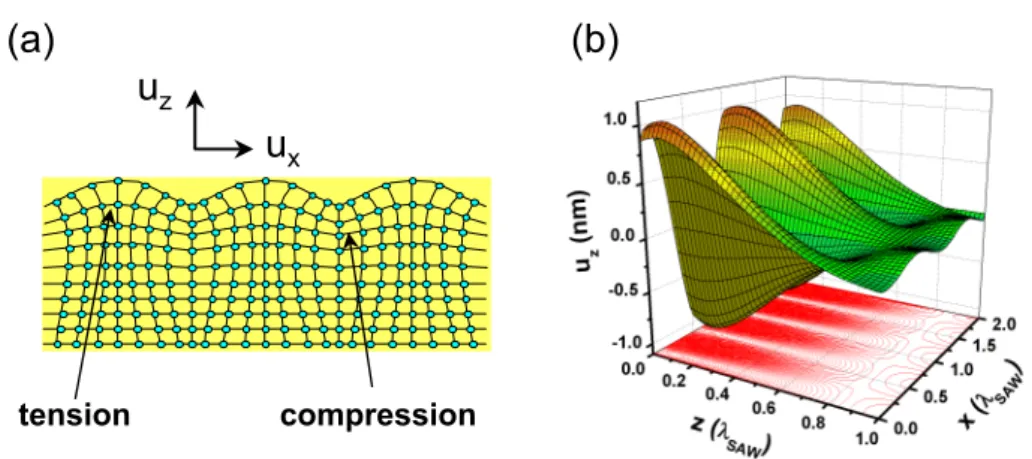
The SAW mode propagating along the [001] direction of a GaAs (110) sur- face is a Rayleigh mode [23]. Rayleigh SAWs consist of a superposition of a longitudinal acoustic (LA) mode with a transverse acoustic (TAz) one po- larized perpendicular to the surface, leading to a displacement field u with components uR = (ux,0, uz)T, as illustrated in Fig. 2.3(a). In general, the amplitudes of the two displacement components ux and uz decrease with depth at different rates. The spatial distribution of the vertical component uzcalculated for a SAW propagating along the [001] direction of the structure in Table 2.1 is displayed in Fig. 2.3(b). For this wave,uz ux. As shown in the figure, the amplitude of the vertical displacement reaches about 1 nm at the surface and decays away from it, with a decay length of approximately λSAW/2.
(a) (b)
tension compression
u
xu
zFigure 2.3: (a) Characteristic particle displacements fields ux and uz of a Rayleigh SAW. (b) Profiles for the vertical displacement uz along the z direction for the Rayleigh wave propagating along the [001] direction of the (110) oriented multilayer structure depicted in Table 2.1. The calculation was performed for λSAW = 5.6µm andPl = 200 W/m.
2.2.3 Propagation along the [1¯10] direction
The SAW mode which propagates along the[1¯10]direction of the (110) sur- face is a Bleustein-Gulyaev wave, which consists essentially of a horizontally polarized shear wave having no displacement component perpendicular to the surface [21, 23, 65]. The displacement pattern for this mode is illus- trated in Fig. 2.4(a). In the sample reference system, this wave is described by a displacement vector given byuBG= (ux,0,0)T. The component ux os- cillates along the propagation directionyˆand decays away from the surface with a longer decay length than the one for the Rayleigh wave componentuz propagating along the [001] direction. As shown in the profile in Fig. 2.4(b), the magnitude of the transverse displacementuxcan reach about 1 nm at the surface and is thus comparable to the surface vertical displacementuz of the Rayleigh SAW in Fig. 2.3(b). The decay length of ux, however, approaches 2λSAW.
2.3 Band structure modulation by SAWs
2.3.1 Strain field
The periodic particle displacement induced by a mechanical wave also gives rise to a modulation of the propagating strain field, as defined by equa-
(b)
x || [001]
z || [110]
y || [110]
_
u
x(a)
Figure 2.4: (a) Particle displacement fieldux for a Bleustein-Gulyaev SAW propagating along the[1¯10]direction of the (110) GaAs surface. (b) Calcu- lated depth dependence ofuxwithPl= 200 W/m for the multilayer structure presented in Table 2.1.
tion (2.3). This is illustrated in Fig. 2.3(a), which shows the lattice vertical displacement modulation by the Rayleigh wave. The spatial modulation of the strain leads to a periodic modulation of the band structure of the under- lying material [42, 120]. The deformation potential modulation of the band gap Eg is caused by local variations of volume and symmetry of the crystal lattice induced by the strain field. In general, Eg reduces in the regions where the crystal is under tension and increases where the crystal is com- pressed, thus creating a periodic band gap modulation along the propagation direction of the SAW.
The (110) surface has two SAW modes with different symmetries propa- gating along the [001] and[1¯10]in-plane directions. It is, therefore, expected that the propagating strain fields [given by equation (2.6)] will have differ- ent effects on the band gap of the underlying material. The strain field for the Rayleigh wave propagating along the xˆ k [001] direction, with the two component displacement vector uR = (ux,0, uz)T, has three non-zero com- ponents. Using the abbreviated notation, the strain fieldSR can be written as:
SR= (Sxx, 0, Szz, 0, 2Sxz, 0)T, (2.11) where the zero components appear becauseuy =∂ux/∂y=∂uz/∂y= 0.
In contrast, the displacement field uBG = (ux,0,0)T for the Bleustein- Gulyaev wave propagating along the yˆ k [1¯10] direction has only one non-
vanishing component. In the sample reference frame, the strain fieldSBGfor this wave has only two non-zero components given by:
SBG = (0, 0, 0, 2Sxz, 0, 2Sxy)T . (2.12) The band-edge states of the conduction (CB) and valence (VB) bands have different symmetries and, accordingly, respond in different ways to the acoustic field. The CB states are s-like and primarily sensitive to the volume changes introduced by the hydrostatic strain componentS0=Sxx+Syy+Szz. The shift in the CB energy is given by ∆ECB = aCBS0, where aCB is the hydrostatic CB deformation potential. The VB states are also modified by S0. In general, however, the energy shifts of the VB are much smaller than the ones for the CB for most semiconductors due to the smaller values for the hydrostatic deformation potential of this band. The VB states are also sensitive to uniaxial strain components, which change the energy and mix heavy-hole (hh) and light-hole (lh) levels. In the case of the strain modulation induced by a Rayleigh SAW, the energy shift due to strain can be written as [42]:
∆Eg= (aCB+aVB)S0±bVB
Szz−Sxx
2
, (2.13)
where the deformation potential of the conduction band aCB is typically about ten times larger thanaVB, the hydrostatic deformation potential of the valence band [149]. The signs + and - apply forhhandlh states, respectively.
The VB uniaxial deformation potentialbVBaccounts for the mixing between thehh andlh states. For QWs, the second term of equation (2.13) becomes relevant only at very high acoustic powers, when the strain-induced shifts become comparable to the splitting between thehh and lh levels associated with the confinement.
Since the CB modulation is mainly affected by S0, the band gap mod- ulation should be small for the Bleustein-Gulyaev waves whereS0 vanishes [compare equations (2.11) and (2.12)]. In this case, the band modulation becomes dominated by shear strain components, which do not affect the CB. The calculation of the band gap modulation in our multilayer struc- ture will be presented in the next subsection, where we discuss the transport mechanisms and the effects of the SAW piezoelectric field.
2.3.2 Piezoelectric field
The moving piezoelectric field which follows the strain plays a key role in the carrier capture and transport processes. In this subsection, we will discuss the distribution of piezoelectric fields in our sample and show how these fields can be enhanced by coating the sample with a piezoelectric ZnO layer.
Like the strain field, the SAW piezoelectric potentialφsaw is modulated along the SAW propagation direction. This field induces a type-II potential modulation of the band edges, which spatially separates optically generated electrons (e) and holes (h) and traps them in the maxima and minima of φsaw, respectively. Figure 2.5 illustrates the type-II modulation created by the piezoelectric field after the optical excitation of electrons and holes with energy¯hω. The spatial separation reduces the overlap between the electron and hole wavefunctions, thus increasing the carrier lifetimes. Long lifetimes allow for long acoustic transport distances.
0.0 0.7 1.4 2.1 2.8 3.5 4.2 4.9 5.6
-1.0 -0.8 -0.6 -0.4 -0.2 0.0 0.2 0.4 0.6 0.8 1.0
φφφφSAW (arb. units)
x (µµµµm)
ω h
v
SAWFigure 2.5: Carrier transport mechanism: the SAW piezoelectric field in- duces a moving type-II potential modulation, spatially separating the opti- cally generated carriers (electrons are denoted by ’-’ and holes by ’+’). ¯hω corresponds to the photon energy used to excite the electron to the CB.
The transport efficiency can be discussed by analyzing the amplitude of φsaw in the QW, which determines the carrier confinement into the SAW po- tential during transport. Figure 2.6(a) shows the depth dependence ofφsaw for the Rayleigh SAW propagating along [001], as well as for the Bleustein- Gulyaev wave propagating along the[1¯10]direction. The profiles were calcu- lated for the multilayer structure presented in Table 2.1 excluding the ZnO
![Figure 2.2: Linear dispersion calculated for the surface acoustic modes along the xˆ k [001] and y ˆ k [1¯ 10] directions of the (110) QW structure described in Table 2.1](https://thumb-eu.123doks.com/thumbv2/1library_info/5579242.1690267/34.892.287.607.329.562/figure-linear-dispersion-calculated-acoustic-directions-structure-described.webp)
![Figure 2.4: (a) Particle displacement field u x for a Bleustein-Gulyaev SAW propagating along the [1¯ 10] direction of the (110) GaAs surface](https://thumb-eu.123doks.com/thumbv2/1library_info/5579242.1690267/36.892.188.704.188.409/figure-particle-displacement-bleustein-gulyaev-propagating-direction-surface.webp)
![Figure 2.6: Calculated depth profiles for the piezoelectric potential amplitude φ saw for the acoustic modes propagating along the [001] and [1¯ 10] directions for the multilayer structure presented in Table 2.1 (a) without ZnO and (b) with the 500 nm thic](https://thumb-eu.123doks.com/thumbv2/1library_info/5579242.1690267/40.892.282.610.467.984/calculated-piezoelectric-potential-amplitude-propagating-directions-multilayer-structure.webp)
![Figure 2.7: Calculations for the out-plane component E z in one SAW cycle for propagation along the [001] (filled dots) and [1¯ 10] (squares) directions for the structure presented in Table 2.1](https://thumb-eu.123doks.com/thumbv2/1library_info/5579242.1690267/41.892.271.613.192.446/figure-calculations-component-propagation-squares-directions-structure-presented.webp)
![Figure 3.6: Effective magnetic field induced by the SAW fields during acous- acous-tic transport in (110) QWs along the (a) [001] and (b) [1¯ 10] directions.](https://thumb-eu.123doks.com/thumbv2/1library_info/5579242.1690267/69.892.187.707.839.1013/figure-effective-magnetic-field-induced-fields-transport-directions.webp)