in Disordered
Quantum Wells and Nanowires
DISSERTATION
Zur Erlangung des
DOKTORGRADES DER NATURWISSENSCHAFTEN (DR. RER. NAT.) der Fakultät für Physik der Universität Regensburg
vorgelegt von
Michael Dieter Kammermeier
aus Regensburg im Jahr 2018
Prüfungsausschuss: Vorsitzender: Prof. Dr. Dominique Bougeard 1. Gutachter: Prof. Dr. John Schliemann
2. Gutachter: Prof. Dr. Thomas Schäpers (FZ Jülich) weiterer Prüfer: Prof. Dr. Klaus Richter
Termin des Promotionskolloquiums: 18.09.2018.
“Not only is the universe stranger than we think, it is stranger than we can think.”
— Werner Heisenberg.
A central theme in semiconductor spintronics is the control of spin-polarized charge carriers. In order to utilize the spin for information processing, a long spin lifetime is essential. In this thesis, we address this issue for important types of semicon- ductor systems: disordered quantum wells and nanowires. Typically, the most prominent process that limits the spin lifetime in inversion-asymmetric systems is the D’yakonov-Perel’ mechanism. It results from the random spin precessions due to the combined effect of impurity scattering and spin-orbit coupling. One very convenient experimental tool to gather information about the spin-relaxation prop- erties, as well as transport parameters, are magnetoconductance measurements of the weak (anti)localization. In particular, the latter is mainly determined by the spin lifetime of the long-lived spin states.
After giving a comprehensive introduction of the underlying theoretical funda- mentals, we identify spin-preserving symmetries in quantum wells of zinc-blende structure. First, we focus on electron systems and prove that persistent spin states can be found due to the interplay of Rashba and Dresselhaus spin-orbit coupling if at least two growth-direction Miller indices agree in modulus. Additionally, a general closed-form expression for the weak (anti)localization is provided to en- able an experimental verification. Secondly, we show that also in [001]-oriented hole systems such symmetries can be realized if in addition uniaxial shear strain is present.
Semiconductor nanowires can have very distinct mesoscopic characteristics. We concentrate on three important kinds of nanowires with diffusive transport chan- nels: (i) tubular zinc-blende nanowires as well as cylindrical (ii) zinc-blende and (iii) wurtzite nanowires. In each of these cases, the impact of a gate-induced Rashba effect is taken into account which allows an external manipulation of the spin relaxation. Employing a Cooperon-based approach, we theoretically analyze the spin-relaxation features, identify the long-lived spin states, and compute the weak (anti)localization correction. The obtained expressions for both types of zinc-blende nanowires are fitted to the experimental data of magnetoconductance measurements of InAs nanowires. We find good agreement between theory and ex- periment and extract reasonable transport parameters. Regarding the spin relax- ation, in contrast to the cylindrical counterpart, the tubular zinc-blende nanowires exhibit a growth-direction dependence. In the cylindrical channels, the spin re- laxation is sensitive to the wire diameter and suppressed in narrow wires due to boundary-induced motional narrowing. The suppression is particularly pronounced in wurtzite nanowires as the relaxation due to the intrinsic linear-in-momentum spin-orbit terms becomes ineffective. Yet, the corresponding long-lived spin states possess a complex helical spin texture which is difficult to realize. This can yield very dissimilar values for the spin lifetimes when extracted from distinct experi- ments. We explicitly demonstrate the arising discrepancies for optical and magne- totransport measurements.
A major part of the present thesis also appears in the following publications:
[1] F. Dirnberger,M. Kammermeier, J. König, M. Forsch, P. E. Faria Junior, T. Campos, J. Fabian, J. Schliemann, C. Schüller, T. Korn, P. Wenk, D.
Bougeard,
Ultralong Spin Lifetimes in One-Dimensional Semiconductor Nanowires, to be published,
[2] M. Kammermeier, P. Wenk, F. Dirnberger, D. Bougeard, and J. Schliemann, Spin Relaxation in Wurtzite Nanowires,
Phys. Rev. B 98, 035407 (2018),
[3] M. Kammermeier, P. Wenk, J. Schliemann, S. Heedt, T. Gerster, and Th.
Schäpers,
Magnetoconductance Correction in Zinc-Blende Semiconductor Nanowires with Spin-Orbit Coupling,
Phys. Rev. B 96, 235302 (2017),
[4] M. Kammermeier, P. Wenk, and J. Schliemann, Control of Spin Helix Symmetry in Semiconductor Quantum Wells by Crystal Orientation,
Phys. Rev. Lett. 117, 236801 (2016),
(selected for the front cover of issue 23, vol. 117)
HYSICAL EVIEW ETTERS
P R L
American Physical Society Member Subscription Copy
Library or Other Institutional Use Prohibited Until 2017 Articles published week ending2 D ECEMBER 2016
Volume 117, Number 23 Published by
[5] M. Kammermeier, P. Wenk, J. Schliemann, S. Heedt, and Th. Schäpers, Weak (Anti-)Localization in Tubular Semiconductor Nanowires with Spin- Orbit Coupling,
Phys. Rev. B 93, 205306 (2016), ( Editor’s Suggestion)
[6] P. Wenk,M. Kammermeier, and J. Schliemann,
Conserved Spin Quantity in Strained Hole Systems with Rashba and Dressel- haus Spin-Orbit Coupling,
Phys. Rev. B 93, 115312 (2016),
[7] T. Dollinger, M. Kammermeier, A. Scholz, P. Wenk, J. Schliemann, K.
Richter and R. Winkler,
Signatures of Spin-Preserving Symmetries in Two-Dimensional Hole Gases, Phys. Rev. B. 90115306 (2014).
Also, due to their relevance, revised sections of my Master thesis, Ref. [8], on Strained Hole Systems with Rashba and Dresselhaus Spin-Orbit Coupling, submit- ted in 2014 at the University of Regensburg, were adopted.
The related research results have been presented in form of oral or poster contri- butions at the following conferences, workshops, Winterschools, and journal clubs.
2018:
• DPG Meeting in Berlin, Germany, Talk.[3]
• International Winterschool in Mauterndorf, Austria, Poster.[3]
2017:
• Journal Club at CNyN in Ensenada, Mexico, Talk.[4]
• SPIE X in San Diego, USA, Poster. [4]
• International Workshop on 1D Systems in Regensburg, Germany,Poster.[4,5]
• International Workshop on Collective Spin Transport in Natal, Brazil,Poster.[4]
• DPG Meeting in Dresden, Germany, Poster. [4]
• NTSD Workshop in Sao Carlos, Brazil, Talk& Poster.[4]
2016:
• International Workshop on Emergent Relativistic Effects in Regensburg, Ger- many, Talk &Poster. [4–6]
• PASPS 9 in Kobe, Japan, Poster. [5]
• ICPS in Beijing, China, Poster.[5] (FBest-Poster-Award Winner)
• DPG Meeting in Regensburg, Germany, Poster. [5]
• International Winterschool in Mauterndorf, Austria, Poster.[5]
2015:
• Journal Club at CNyN in Ensenada, Mexico, Talk.[6,7]
• Gordon Research Seminar and Conference in Hong Kong, China, Talk &
Poster. [6,7]
• DPG Meeting in Berlin, Germany, Talk.[6,7]
List of Symbols 1
Introduction 3
I Theoretical Foundation 9
1 Band Structure of Semiconductors 11
1.1 The Origin of Spin-Orbit Coupling . . . 11
1.2 k·p Method and the Envelope Function Approximation . . . 13
1.3 Extended Kane Model . . . 16
1.4 Effective Electron and Hole Hamiltonian . . . 21
1.4.1 Centrosymmetric Crystals . . . 22
1.4.2 Bulk Inversion Asymmetry . . . 23
1.4.3 Structure Inversion Asymmetry . . . 25
1.4.4 Quantum Confinement . . . 28
1.4.5 Quantum Wells of General Crystal Orientation . . . 31
1.5 Strain Effects . . . 33
1.5.1 Relation between Strain and Stress . . . 34
1.5.2 Strain ink·p Theory . . . 37
Appendix 1.A Löwdin Perturbation Theory . . . 40
Appendix 1.B Spin and Total Angular Momentum Matrices . . . 41
Appendix 1.C Parameters and Spin-Orbit Coupling Coefficients . . . 42
Appendix 1.D 6×6 Kane Model. . . 45
2 Types of Spin-Relaxation Processes 47 2.1 D’yakonov-Perel’ Mechanism . . . 47
2.2 Elliott-Yafet Mechanism . . . 51
2.3 Bir-Aronov-Pikus Mechanism . . . 52
2.4 Hyperfine Interaction. . . 53
3 Quantum Transport Corrections 55 3.1 Kubo Formula for the Conductivity. . . 55
3.1.1 Linear Response Theory . . . 55
3.1.2 Electrical Conductivity Tensor . . . 56
3.1.3 Longitudinal Static Conductivity . . . 57
3.2 Diagrammatics in Disordered Systems . . . 58
3.2.1 Green’s Functions and the Dyson Equation . . . 58
3.2.2 Impurity-Averaged Propagator . . . 61
3.3 Conductivity for Weak Disorder. . . 63
3.3.1 Drude-Boltzmann Conductivity . . . 64
3.3.2 Weak (Anti)Localization. . . 66
Appendix 3.A Auxiliary Function . . . 71
Appendix 3.B Singlet-Triplet Representation . . . 71
Appendix 3.C Sum Formula . . . 72
Appendix 3.D Relation between Triplet Basis and Spin Density Compo- nents. . . 73
II Persistent Spin Textures in Quantum Wells 75 4 Electrons in Quantum Wells with General Crystal Orientation 77 4.1 2D Electron Model Hamiltonian. . . 77
4.2 Spin Diffusion Equation . . . 78
4.3 Conditions for Persistent Spin States . . . 78
4.4 Imprints on Weak (Anti)Localization . . . 81
4.5 Magnetoconductivity near SU(2) Symmetry . . . 82
4.6 Summary . . . 84
Appendix 4.A Key Requirement for Miller Indices . . . 85
Appendix 4.B Impact of Higher Angular Harmonics . . . 86
Appendix 4.C Spin Diffusion Operator for Two Identical Miller Indices . 88 5 Strained 2D Hole Systems 91 5.1 Motivation . . . 91
5.2 Hole Model Hamiltonian . . . 93
5.2.1 Effective 4×4 Hole Hamiltonian . . . 93
5.2.2 Effective 2×2 Model for the First Subband . . . 94
5.2.3 Summarized Results . . . 98
5.3 Conserved Spin Quantity . . . 99
5.3.1 Conserved Spin Quantity in Case of a HH-like Ground State 100 5.3.2 Conserved Spin Quantity in Case of a LH-like Ground State. 103 5.3.3 Example: p-doped InSb . . . 104
5.4 Summary . . . 107
Appendix 5.A Utilized Approximations . . . 109
5.A.2 LH-like Valence Band Ground State: Mixing of the Electric
Field and Dresselhaus Term . . . 110
Appendix 5.B Uniaxial Strain via Piezo Crystals. . . 110
Appendix 5.C Domain . . . 111
III Spin Relaxation and Conductivity in Nanowires 113 6 Zinc-Blende Nanowires with 2D Tubular Conductive Channel 115 6.1 Model Hamiltonian for Tubular 2DEG . . . 115
6.1.1 Bulk Model . . . 115
6.1.2 Coordinate Transformation . . . 116
6.1.3 Tubular System. . . 117
6.1.4 Spin Conservation on the Tubular Surface . . . 120
6.2 Quantum Correction to the Conductivity . . . 121
6.2.1 Cooperon Hamiltonian . . . 121
6.2.2 Spectrum Analysis . . . 123
6.2.3 Magnetoconductivity Correction . . . 129
6.2.4 Experimental Data Fitting: InAs Nanowire . . . 131
6.3 Summary . . . 134
Appendix 6.A Pauli Matrices in Cylindrical Coordinates . . . 137
Appendix 6.B Commutator Relations . . . 137
Appendix 6.C Matrix Elements . . . 137
Appendix 6.D Radial Momentum Expectation Value . . . 137
Appendix 6.E Auxiliary Function in the Tubular System . . . 138
Appendix 6.F Spin-Orbit Coupling Matrices . . . 138
7 Cylindrical 3D-Diffusive Zinc-Blende Nanowires 141 7.1 Formulation of the Bulk Problem . . . 141
7.1.1 Hamiltonian for Bulk Electrons . . . 141
7.1.2 3D Conductivity Correction and Cooperon . . . 142
7.2 Finite-Size Effects on the Diffusion in Mesoscopic Nanowires. . . 143
7.2.1 Impact of a Radial Boundary Condition . . . 143
7.2.2 Zero-Mode Approximation. . . 145
7.2.3 Spin Relaxation in Narrow Wires . . . 146
7.2.4 General Remarks . . . 147
7.3 Magnetoconductance Correction . . . 148
7.3.1 Magnetic Dephasing . . . 148
7.3.2 Zero-Mode Magnetoconductance Correction . . . 149
7.3.3 Experimental Data Fitting . . . 150
7.4 Summary and Perspective . . . 153
Appendix 7.A Zero-Mode Cooperon Hamiltonian . . . 155
Appendix 7.B Experimental Data Fitting with Kurdaket al.’s Formula . 155 8 Cylindrical 3D-Diffusive Wurtzite Nanowires 159 8.1 Theoretical Groundwork . . . 159
8.1.1 Electrons in the Wurtzite Lattice . . . 159
8.1.2 3D Cooperon and the Radial Boundary . . . 160
8.2 Intrinsic Spin Relaxation. . . 162
8.2.1 Spin Relaxation in the Bulk . . . 162
8.2.2 Spin Dynamics in the Nanowire. . . 163
8.2.3 Conclusive Remarks and Example . . . 170
8.3 Magnetoconductance Correction . . . 173
8.3.1 Nanowire with a Lateral Gate Electrode . . . 173
8.3.2 Zero-Mode Magnetoconductance Correction . . . 176
8.4 Summary and Conclusion . . . 176
Appendix 8.A Intrinsic Spin-Orbit Coupling . . . 179
Appendix 8.B Diffusive-Ballistic Crossover . . . 179
Future Prospects 181
Acknowledgments 185
References 187
Throughout this thesis we frequently use the following notations and abbreviations.
Notations
A magnetic field induced vector potential
As spin-orbit induced vector potential
B magnetic field
C/ˆ HˆC Cooperon/Cooperon Hamiltonian
∆G (magneto)conductance correction
∆σ weak (anti)localization correction
De diffusion constant
e >0 electron charge
E electric field
ij strain tensor components
EF/vF/kF Fermi energy/velocity/wave vector
G Green’s function in the first Born approximation
H Hamiltonian
J vector of total-angular-momentum-32 matrices le/τe elastic mean free path/scattering time
lφ/τφ dephasing length/time
ls/τs spin-relaxation length/time lB/τB magnetic dephasing length/time
Lso spin precession length
m0 bare electron mass
m∗ effective electron mass
Ω spin-orbit field
R rotation operator
S vector of spin-1 matrices
σ vector of Pauli matrices
[A, B] =AB−BA commutator {A, B}=AB+BA anti-commutator
{A, B}(s)= 12(AB+BA) symmetrized anti-commutator
Abbreviations
1BA first Born approximation
1D/2D/3D one/two/three-dimensional
2DEG/2DHG two-dimensional electron/hole gas
BIA bulk inversion asymmetry
c.p. cyclic permutation
DP D’yakonov-Perel’
EY Elliott-Yafet
GMR giant magnetoresistance
HH/LH heavy/light hole
MOSFET metal-oxide-semiconductor field-effect transistor
SIA structure inversion asymmetry
SOC spin-orbit coupling
SOF spin-orbit field
WL/WAL weak localization/antilocalization
Although electrons carry charge and spin, in the history of information technology both properties have been employed separately. While classical data storage uses the manifestation of spins as the magnetization of ferromagnets, data processing employs the transport of charges in response to applied electric fields.
This individual focus started to fade in the late 80th with the discovery of the giant magnetoresistance (GMR) by Grünberg and Fert who were jointly awarded the Nobel Prize in 2007. This effect is based on the influence of magnetic materials on charge currents and is used in thespin-valve device. Here a non-magnetic layer is sandwiched between two magnetic layers of either parallel or antiparallel mag- netization. In one magnetic layer, the magnetization is pinned while in the other one it can be rotated by an applied magnetic field. An antiparallel configuration of the two magnetizations yields a significantly larger resistance than the parallel one. This makes it possible to detect tiny magnetic fields even at room temper- ature with high sensitivity and allows to read-out data stored in great density.
As a result, the spin-valve GMR along with other successive devices based on the same principles have triggered a large increase in memory capacity and processing speed and are by now indispensable in state-of-the-art hard disc drives. Yet, the GMR is only a paradigmatic example to demonstrate how the combined utilization of charge and spin can largely impact the modern information world. In fact, a rapidly growing field of research and technology has emerged, which is today well known asspintronics.
While spintronic devices based on magnetic materials have already found its place in the modern data storage industry, spin-dependent data processing devices are yet to be developed. In this context, the most important component is the field-effect transistor, which is predominantly built from semiconductor materials.
Today’s computer processors host millions of transistors. This number follows the trend of an exponentially increasing transistor density on integrated circuits, which was observed already in 1965 by Moore [9]. The continuing miniaturization allowed us to steadily enhance the functionality and processing speed of computer chips without significantly increasing the power dissipation. However, at some point the down-scaling naturally comes to an end. A practical reason is that the channel length between source and drain becomes so short that quantum tunneling makes it possible to transport charge carriers despite a potential barrier. The arising off-state leakage current leads to static power consumption and makes it hard to distinguish between an on-state and off-state (or 1 and 0 in binary language) of the transistor [10–12]. Hence, it becomes apparent that in order to obtain further improvements in functionality or performance, alternative device concepts
Source Drain Gate
(a) VG= 0 (OFF)
Source Drain
Gate
(b) VG6= 0 (ON)
Fig. 1: Datta-Das spin field-effect transistor. (a) Off-state: The injected spins do not precess and are antiparallel to the spin orientation in the drain: The transistor is locked. (b) On-state: The spins precess in a way that they are parallel to the spin orientation in the drain: The transistor is conducting.
are needed which do not rely on classical physical laws. One of the ideas is to develop a device that operates on a more fundamental level, using the spin degree of freedom. In contrast to conventional electronics, we do not manipulate charge currents but the currents of spin-polarized electrons.
A prominent and inspiring example for such a prototypical device is the spin field-effect transistor as proposed by Datta and Das in 1990 [13]. Its functional principle is illustrated in Fig. 1. The source and drain are modeled by ferromag- nets (blue regions) which have a certain fixed antiparallel magnetization. Due to the magnetization, the source injects carriers of a well-defined spin polarization into a gated region (yellow), which is assumed to be a ballistic n-doped semiconductor channel. For a vanishing gate voltage, the spin orientation of the electrons remains unchanged while they are transported through the channel. Since the spin orienta- tion is antiparallel to the magnetization in the drain, the transmission is suppressed and the transistor is locked (cf. Fig.1a). The conducting state can be realized by applying a gate voltage. As a consequence ofRashba spin-orbit coupling, the elec- tron spins precess in the gated region about an angle that is controlled by the gate voltage. If the final spin polarization at the drain is parallel to its magnetization, the electrons can pass through the drain and the transistor is conducting (cf. Fig.
1b).
For practical applications above device yields several conceptual problems and its realization has so far not been too successful although a few working examples have been presented [14, 15]. Aside from the obstacle of inefficient spin injection due to the conductance mismatch at the ferromagnet-semiconductor interface [16], one major issue is that the spin in solids is not a good quantum number. Ironically, the key mechanism that allows for an all-electric manipulation of the spin orien- tation, the spin-orbit coupling, at the same time constitutes the primary source of spin relaxation. Since a realistic semiconductor is rarely free of impurities, the disorder scattering in combination with spin precession due to spin-orbit coupling causes an efficient spin relaxation process called D’yakonov-Perel’ mechanism [17].
coupling, as well as the initial spin polarization texture. Hence, there exist several ways to manipulate the spin relaxation or even suppress it. To identify such sce- narios in semiconductor quantum wells and nanowires constitutes a central theme of this thesis.
One possibility to overcome this issue is to find special parameter configurations which yield spin-preserving symmetries. These symmetries allow for long-lived or even persistent spin states which remain intact in the presence of spin-independent disorder. In a structurally confined two-dimensional electron gas (2DEG) such persistent solutions have been predicted by Schliemann et al. in 2003 [18]. The necessary ingredient is a crystal orientation along the [001]-direction of the zinc- blende lattice and a certain ratio between the linear-in-momentum Dresselhaus and Rashba spin-orbit coupling coefficients. As a consequence, the spin of the electrons traversing the system undergoes a well-defined rotation which is indepen- dent of the propagated path but solely determined by the initial and final posi- tion. The controlled spin rotation opens the possibility to build a spin transistor whose functionality is not only restricted to the ballistic case. This phenomenon is known today aspersistent spin helix [19] and its existence has been unambiguously confirmed in numerous experiments by means of optical and transport measure- ments [20–24]. The latter exploit the impact of spin-orbit coupling on the weak (anti)localization correction to the conductivity. Other systems that are known to host persistent spin states comprise rolled-up as well as [110] and [111]-oriented 2DEGs [25]. Aside from that, spin-preserving symmetries in two-dimensional hole gases (2DHGs) were also predicted but with the requirement for rather unusual bandstructure parameters [7,26]. In this thesis, we determine the necessary con- ditions for such symmetries in zinc-blende 2DEGs of arbitrary crystal orientation and derive analytic expressions for the weak (anti)localization correction to support experimental probing. In particular, it is shown that at least two growth-direction Miller indices have to agree in modulus and the Rashba and Dresselhaus coeffi- cients must be appropriately tuned. Moreover, it is demonstrated that persistent spin states can be also found in [001]-oriented zinc-blende 2DHGs for realistic pa- rameter configurations if a uniaxial shear strain is present.
Modern techniques enable the fabrication of semiconductor devices at the na- noscale. At this size, the dephasing length can become comparable to the system size and the effects of coherent quantum mechanics become important. And yet, at the same time, these systems are often too large and complex for a pure micro- scopic description. In this so-called mesoscopic regime, quantum effects are often combined with statistical and classical features [27]. Here, the quantum interfer- ence correction to the Drude conductivity, the weak (anti)localization, is a prime example. The properties of a mesoscopic system crucially depend on the relation of the characteristic length scales, such as the system size, the Fermi wavelength, the dephasing length, the elastic mean free path, and - for spin-related phenom- ena - the spin precession length. Nanowires are typical objects that fall into that mesoscopic range.
Semiconductor nanowires are very popular within the nanoscience community as they form the cornerstone for several fundamental discoveries [28–31] and repre- sent a key element of future electronic and spintronic devices [32–40]. To support this technical progress, a sound knowledge and reliable control of the system’s transport parameters, the spin-orbit coupling, and the spin relaxation are essen- tial. Low-field magnetoconductance measurements of the weak (anti)localization provide convenient access to the desired information [41–50]. Since the weak (anti)localization characteristics are primarily determined by the spin-relaxation minima, they are particularly suited to determine the lifetime of the long-lived spin states. The method requires experimental data fitting with the appropriate theoretical model, which depends on the mesoscopic details of the system. Yet, this becomes problematic since the huge degree of freedom in the device preparation process allows to manipulate many of the nanowire properties over a wide range.
More precisely, one is able to effectively control the size, morphology, potential landscape, carrier and impurity concentration, or even crystal structure [51–60].
The great diversity makes it difficult to build up a general suitable theoretical de- scription of the weak (anti)localization correction. In fact, a variety of theoretical models is needed to appropriately characterize the differing nanowires.
In the diffusive regime, where the elastic mean free path is much smaller than the system size, the weak (anti)localization was analyzed by Kettemann for pla- nar quantum wires with a zinc-blende lattice [61]. In accordance with other stud- ies [21,62–67], it is shown that the D’yakonov-Perel’ spin-relaxation process suffers a considerable slowdown for certain spin polarizations in narrow wires of widths much smaller than the spin precession length. This results from motional narrowing due to spin-conserving scattering at the boundaries and becomes relevant as soon as the wire width is shorter than the dephasing length. Complimentary to this, the present thesis covers an important class of diffusive semiconductor nanowires with spin-orbit coupling. Analytical expressions are derived for the magnetoconductance correction due to weak (anti)localization and the D’yakonov-Perel’ spin-relaxation rates. Depending on the type of surface states, the doping, or the appropriate bandgap engineering in core/shell nanowires, the electrons form either a tubular or cylindrical conductive channel [55,59,68]. We develop theoretical models for zinc- blende systems accounting for both situations and employ them to fit experimen- tal data of magnetoconductance measurements. The comparison with experiment shows good agreement and delivers reasonable transport parameters. In the last chapter, we provide an analogous model for wurtzite nanowires with a cylindrical diffusive channel. With regard to spin-relaxation properties, we observe that the tubular zinc-blende nanowires exhibit a growth-direction dependence opposed to the cylindrical counterpart. Similar to the planar quantum wires, the finite wire diameter yields a suppression of the spin relaxation in the cylindrical systems. The impact of the boundary is particularly pronounced in wurtzite due to the presence of linear-in-momentum spin-orbit terms. As a consequence, the intrinsic spin re- laxation can be significantly reduced in comparison to the bulk system. At the same time, the corresponding long-lived spin states assume a complex helical spin texture which is sensitive to the system parameters and difficult to realize. This
This thesis is falls into three parts:
• Part I: Theoretical Foundation
In the first part, we introduce the relevant theoretical fundamentals. We discuss the bandstructure in zinc-blende and diamond-type semiconductors with a particular focus on the spin-orbit effects. Also, the most important spin-relaxation phenomena are briefly described. At last, we give a detailed derivation of the weak (anti)localization correction which is based on linear response theory and Green’s function techniques.
• Part II: Persistent Spin Textures in Quantum Wells
In the second part, we focus on the identification of system configurations which yield spin-preserving symmetries. The investigated objects comprise electrons and holes in two-dimensional zinc-blende quantum wells with Rashba and Dresselhaus spin-orbit coupling. In case of holes, the ramifications of strain are also considered.
• Part III: Spin Relaxation and Conductivity in Nanowires
In the last part, we perform a detailed study of the spin-relaxation properties and the weak (anti)localization correction to the conductivity in semicon- ductor nanowires. We cover diffusive tubular zinc-blende systems and diffu- sive cylindrical transport channels with an underlying zinc-blende or wurtzite lattice.
Theoretical Foundation
CHAPTER
1
Band Structure of Semiconductors
1.1 The Origin of Spin-Orbit Coupling
In contrast to traditional electronics, spintronics exploits the spin degree of freedom of the electron in addition to its charge. The essential effect, which allows an effective control of the spin, is the spin-orbit coupling (SOC). For this reason, it is quite illuminating to recall its origins.
It can be traced back to the Lorentz-invariant formulation of quantum mechan- ics. Here, electrons and positrons with spin-1/2 are simultaneously described by theDirac equation, which can be written in the stationary case as
(cα·p+β m0c2+V 14×4) |ψi=E |ψi, (1.1) where
α=
0 σ σ 0
, β =
12×2 0 0 −12×2,
,
pdenotes the kinetic momentum,m0 the bare electron mass,cthe speed of light in vacuum,σ the vector of Pauli matrices,E the energy, and|ψithe four-component spinor. The potentialV is considered in this context as purely electrostatic as we are interested in the interaction with atomic potentials, i.e.,V =V(r). We further include electromagnetic interactions by substitutingp→pc+eAwith the canonical momentum pc=−i~∇. The above matrix representation assumes the basis order {|A↑i,|A↓i,|B ↑i,|B ↓i}, where A labels the electrons,B the positrons and the arrow the spinz-component. It becomes obvious, that the mixing of the different spin species occurs only due to the coupling of electrons and positrons. In the following, we apply Löwdin perturbation theory (cf. App.1.A) to derive an effective HamiltonianHeA for the electrons that perturbatively includes the spin mixing.
At rest, the electron and positron branches are separated by the energy gap
∆ = 2m0c2. In the non-relativistic limit, this gap largely exceeds the kinetic energy and we may decompose the Dirac Hamiltonian as
H0 =β m0c2, (1.2)
H0 =cα·p+V 14×4, (1.3)
whereH0 constitutes a small perturbation to H0. SinceH0 is diagonal in the given basis, the effective HamiltonianHeA for the electrons yields in third-order Löwdin perturbation theory, according to Eqs. (1.A.3)-(1.A.6),
HeA= H(0)A +H(1)A +H(2)A +H(3)A , (1.4) with
H(0)A =m0c212×2, (1.5)
H(1)A =V 12×2, (1.6)
H(2)A = p2
2m0 12×2+ e~
2m0
σ·B, (1.7)
H(3)A = e~2
8m2c2∇ ·E12×2− e~
4m2c2σ·(p×E), (1.8) whereB=∇ ×Ais the magnetic field associated with the vector potentialAand E= 1e∇V the internal electric field.
Including terms up to second-order gives rise to the Pauli equation,1 which extents the (non-relativistic) Schrödinger equation by taking into account the in- teraction of the electron spin with an external electromagnetic field [69]. Respon- sible for this coupling is the second term in H(2)A , which is denoted as Zeeman term. It underlines the close relation of the electron spin S and the magnetic moment µ, which becomes obvious through the substitution µ = −gµBS/~ and S = ~2σ, where µB = 2me~0 is the Bohr magneton and g ≈2 the electron g-factor.
It is common practice to rewrite the SOC term as Zeeman term with an effec- tive momentum-dependent magnetic field Beff and a modified effective g-factor.
Third-order relativistic corrections include the Darwin term and the SOC term, the first and second term in H(3)A , respectively. These two terms reflect the non- commutativity of p and V, that is, [p, V] = −ie~E [70]. The Darwin term is related to theZitterbewegung of the relativistic electron and is relevant in the fine structure of s-type atomic orbitals [71]. Our major interest concerns the second term inH(3)A , which represents the SOC and will be labeled byHso hereafter. For convenience, we will frequently rewrite it in terms of aspin-orbit field (SOF)Ω(k) withk=p/~, that is,
Hso=Ω(k)·σ. (1.9)
As previously mentioned, we are interested in the influence of atomic potentials, which means, in general, an average Coulomb field of the nuclei and the other electrons. For an approximately radial symmetric electrostatic potential V(r) =
−eφ(r) and the according electric fieldE =−(dφ/dr)er, the SOC can be rewritten in terms of the orbital angular momentumL as
Hso=− e~
4m20c2σ·(p×E)
1The rest energy is usually excluded.
=− e~ 4m20c2
1 r
dφ dr
σ·(r×p)
=λS·L, (1.10)
withλ=− e
2m20c2 1 r
dφ
dr. In this form, the coupling of the spin to the orbital angular momentum becomes obvious. Notably, the above expression can also be derived in classical relativistic electrodynamics by taking into account the Thomas preces- sion [72].
Summarizing, we see that the intrinsic degree of freedom, the spin, emerges from the non-relativistic approximation to the Lorentz-invariant description of fermions in quantum mechanics. The resulting SOC HamiltonianHsois essential for describ- ing the electronic band structure in a solid, which will be the task of the following section.
1.2 k· p Method and the Envelope Function Approximation
Beyond question, the most important material class for building data processing devices is the semiconductor. The fundamental property that distinguishes semi- conductors from other materials is the small energy gap between conduction and valence band (typically<3 eV), which opens vast possibilities for external manip- ulation. A prime example of this is the transistor, which allows switching between a conducting and an insulation state by applying a gate voltage. Therefore, it is of central importance to have a sophisticated understanding of its unique band structure, which will be investigated in the following.
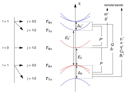
Several different methods have been developed to model the band structure in a semiconductor, such as the free electron model, the pseudopotential method, tight-binding or LCAO (Linear Combination of Atomic Orbitals) approach, or the k·p method. Each of these computation techniques involves approximations that tend to emphasize some aspect of the electronic properties while at the same time de-emphasizing others [73]. Most suitable for our purpose will be thek·pmethod and its generalization the Envelope Function Approximation (EFA). This method can deal with distinct geometries of quantum structures and perturbations such as magnetic fields, strain, and internal or external potentials. It provides a comprehen- sive analytical description of the band dispersion in the vicinity of a givenk0-point in the Brillouin zone and pictures subtleties like non-parabolicity, spin splitting, and coupling between heavy and light hole-like states [70]. The obtained analytical expressions are related to optical matrix elements and energy gaps, which can be directly extracted from experiments. Usually, the expansion pointk0 corresponds to a high-symmetry point in the Brillouin zone, which allows taking advantage of symmetry properties of the crystal lattice. Thereby, the number of contributing input parameters can be significantly reduced [16]. The physics of semiconductors is predominantly determined by the states close to the band extrema. In direct bandgap semiconductors, which are important for spintronics, such as GaAs, InAs,
or InSb, the valence band maximum, and the conduction band minimum are lo- cated at the Γ-point, i.e.,k0= 0, which is, therefore, the relevant symmetry point to determine many properties of the materials [74].
The Schrödinger equation for Bloch electrons in the microscopic lattice-periodic potentialV0(r) in absence of any fields forms the basis of both thek·ptheory and the EFA. For the Bloch functions Ψνk(r) =eik·ruνk(r), it reads as
"
p2
2m0 +V0(r)
#
Ψνk(r) =Eν(k) Ψνk(r), (1.11) whereuνk(r) =hr|νki is the lattice-periodic part, k the wave vector, ν the band index, andm0 the free electron mass. The principle idea now consists of expand- ing the lattice periodic part|νki in terms of known band edge functions {|νk0i}, which constitute a complete orthonormal basis. In the following, we give a brief description of the EFA formalism, which is more general than thek·p approach as it also accounts for spatial dependent fields. A consideration of these fields is, for instance, essential to explain the Rashba spin splitting in inversion-asymmetric quantum wells, an effect that is of central importance in this work.
From here on, let us consider a semiconductor crystal lattice in the presence of electric and magnetic fields that modulate slowly in comparison with the lat- tice constant. As shown in the previous section, the Schrödinger equation with relativistic corrections (disregarding the Darwin term and the rest energy) reads as
p2
2m0 +V(r)− ~
4m20c2σ·(p× ∇V(r)) +µBσ·B
!
Ψ(r) =EΨ(r), (1.12) wherep =−i~∇+eA(r) denotes thekinetic momentum and B =∇ ×A(r) the magnetic field with the according vector potentialA(r). The potentialV =V0+V1
is composed of the lattice-periodic potentialV0(r) and an additional potentialV1(r), which typically results from built-in or external electric fields as well as step-like potentials2due to the position-dependent band edges in heterostructures. Since the strong Coulomb potentialV0in the vicinity of the atomic core region largely exceeds V1, we can drop the latter in the SOC term. As mentioned above, we expand the wave functions in terms of band edge functions including the spin degree of freedom
|σ0i, that is,
Ψ(r) = X
ν0,σ0
φν0,σ0(r)uν00(r)|σ0i, (1.13) where we set k0 = 0. The expansion coefficients φν0,σ0(r) comprise the slowly varying spatial dependence ofV1 andAand are called envelope functions. By way of illustration, we sketch a wave function Ψ(r) in Fig.1.1, which might appear in a
2The inclusion of step-like potentials appears here to be a violation of the requirement for a slowly modulating potential. Yet, the excellent agreement of the theoretical predictions with the experimental results justifies the application of EFA also in such scenarios [74].
![Fig. 2.3: Persistent spin textures in real space for in a 2DEG grown along [001]](https://thumb-eu.123doks.com/thumbv2/1library_info/3940808.1533236/69.892.137.709.108.380/fig-persistent-spin-textures-real-space-deg-grown.webp)
![Fig. 4.1: (a) Global minimum λ min (in terms of Q so = 4 mβ (1) / ~ 2 ) of the spectrum of the spin diffusion operator Λ sd for the optimal ratio of Rashba and Dresselhaus coefficients α/β (1) for different growth directions [˜ n x , n˜ y , 5] (˜ n x , n˜](https://thumb-eu.123doks.com/thumbv2/1library_info/3940808.1533236/97.892.248.657.212.889/global-spectrum-diffusion-operator-dresselhaus-coefficients-different-directions.webp)
![Fig. 4.3: 2DEG grown along [113] for c e /c φ = 10 3 and c e = 1 with α/β (1) close to the SU(2) symmetry point](https://thumb-eu.123doks.com/thumbv2/1library_info/3940808.1533236/101.892.221.691.235.840/fig-deg-grown-φ-close-su-symmetry-point.webp)
