in the regime of the persistent spin helix
Dissertation
zur Erlangung des Doktorgrades der Naturwissenschaften (Dr. rer. nat.)
der Fakultät für Physik der Universität Regensburg
vorgelegt von Sven Gelfert aus Bayreuth
im Jahr 2020
Prüfungsausschuss: Vorsitzender: Prof. Dr. Gunnar Bali
1. Gutachter: Prof. Dr. Christian Schüller
2. Gutachter: Prof. Dr. Sergey Ganichev
weiterer Prüfer: Prof. Dr. Josef Zweck
1 Introduction 1
2 Basics 5
2.1 GaAs-AlGaAs heterostructures . . . . 5
2.1.1 Crystal structure of GaAs . . . . 5
2.1.2 Electronic band structure . . . . 6
2.1.3 Quantum well structure . . . . 7
2.2 Sample growth and design . . . . 9
2.2.1 MBE growth . . . . 9
2.2.2 Investigated samples . . . . 10
2.3 Spin-orbit interaction . . . . 17
2.3.1 Bulk inversion asymmetry - BIA . . . . 19
2.3.2 Structure inversion asymmetry - SIA . . . . 21
2.3.3 The persistent spin helix . . . . 23
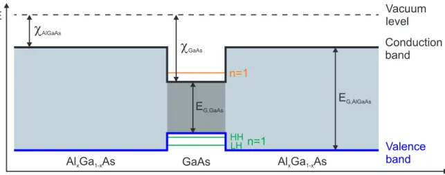
2.4 Inelastic light scattering on 2DES . . . . 26
2.4.1 Elementary electronic excitations in 2DES . . . . 27
2.4.2 Resonant scattering processes . . . . 31
2.4.3 Intrasubband SDEs in [001]-grown quantum wells . . . . 35
2.5 Two-dimensional electronic systems in external magnetic fields . . . . . 38
2.5.1 Superposition of the intrinsic spin-orbit field with external in- plane magnetic fields . . . . 38
2.5.2 Landau quantization . . . . 40
3 Methods 43 3.1 Experimental setup . . . . 43
3.1.1 Magnetocryostat . . . . 45
3.1.2 Cryostat insert . . . . 47
3.1.3 Measurement geometry . . . . 47
3.2 Computational Lindhard-Mermin line-shape analysis . . . . 50
3.2.1 Basic considerations . . . . 50
3.2.2 Transformations of the Lindhard-Mermin response function . . . 52
3.2.3 Numerical evaluation of the integrals . . . . 53
3.2.4 Including the spin-orbit field of the persistent spin helix . . . . . 55
3.2.5 Including an external in-plane magnetic field . . . . 57
4 Experimental results 59 4.1 Introduction . . . . 59
4.2 Sample characterization . . . . 59
4.2.1 Photoluminescence . . . . 60
4.2.2 Resonances of spin-density excitations . . . . 62
4.2.3 Excitation-dependent temperature of the 2DES . . . . 66
4.3 Electrical gating . . . . 68
4.3.1 I-V characteristics . . . . 69
4.3.2 Photoluminescence response . . . . 70
4.3.3 Electronic Raman response: Tuning of the Bychkov-Rashba pa- rameter . . . . 72
4.4 Out-of-plane external magnetic fields: Magneto luminescence . . . . 77
4.4.1 Determination of the charge-carrier density . . . . 77
4.4.2 Effect of electrical gating . . . . 78
4.5 Out-of-plane external magnetic fields: Spin-density excitations . . . . . 80
4.5.1 Near resonant magnetic field sweep: overview . . . . 81
4.5.2 SDE response and cyclotron resonances . . . . 82
4.5.3 Nonspinflip excitations: Polarized measurement geometry . . . . 87
4.6 In-plane external magnetic fields . . . . 89
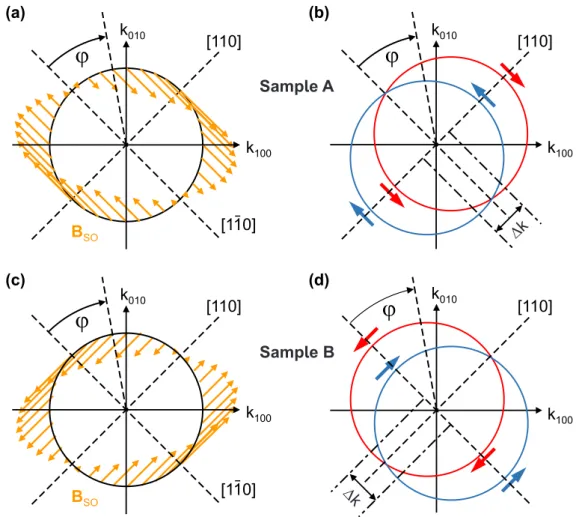
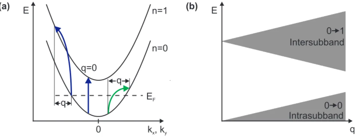
4.6.1 Angular mapping of the spin-splitting anisotropy . . . . 90
4.6.2 Determining the intrinsic effective spin-orbit field strength . . . 96
5 Conclusion 101
Bibliography 103
List of publications 116
Conference contributions and invited talks 117
Chapter 1
Introduction
The fast progress of digitalization and connectivity is encountering increasingly complex limits in its technical realization. Not only in the aspect of environmental protection we are obliged to design modern technologies in a resource-saving and energy-efficient man- ner. It is also important to develop better encryption techniques to ensure data security in the future. The progress in information technology has been mainly dominated by semiconductor-based devices, where data encoding and processing is implemented by means of the electrical charge of electrons. Since the development of the first transistor in the year 1948 [Bar48] and the invention of integrated electric circuits [Kil63, Kil76]
with a structure size in the micrometer range, advances in information technology have so far been achieved by scaling down the device sizes and reaching higher transistor densities. Modern conventional CMOS
1transistors are approaching length scales of single atoms and molecules, where parasitic resistances and capacitances [Tho06], as well as quantum mechanical tunneling of charge carriers are limiting factors. This is associated with an increasing power consumption and an uncontrollable heat produc- tion of modern devices. The demand for more computing power is thus in contrast to an energy-efficient future and requires new concepts.
Interestingly, a possible way out might me to harness complex quantum mechanical effects instead of viewing them as an invincible barrier. A very promising candidate is the field of the semiconductor-based spintronics, where the magnetic dipole moment of electrons is utilized instead of their charge. This field was pioneered by P. Grün- berg and A. Fert in the year 1988 with the discovery of the giant magnetoresistant (GMR) effect [Bai88, Bin89]. The implementation of this technology in commercial hard drives enabled a drastic increase of the storage capacity and paved the way for
1
CMOS: complementary metal oxide semiconductor
a rapid development in computer technology. Another very prominent concept in the field of spintronics was proposed by S. Datta and B. Das in the year 1990: the so- called spin field-effect transistor [Dat90]. In such a device, spin-polarized electrons are injected into a semiconducting channel where they travel ballistically to a detection contact. Inside this channel region, dominated by spin-orbit coupling, the spins perform a precession movement, which can be manipulated via an external gate. Because of a
“spin-dependent” transmission, the spin at the detection contact is either blocked or let passed, depending on its orientation. This corresponds to the off/on state of a tran- sistor. The realization of such a device was demonstrated at operating temperatures in the millikelvin range [Koo09]. However, the ballistic electron transport makes the controllability of the spin precession very error-prone and impedes its commercial real- ization. A promising candidate to circumvent this problem is the so-called nonballistic spin transistor, proposed in the year 2003 by J. Schliemann [Sch03]. It takes advantage of a unique spin-orbit field symmetry, arising from an interplay of the Bychkov-Rashba [Byc84b] and the Dresselhaus [Dre55] spin-orbit field. By balancing the strengths of both contributing fields, the spins arrange in a helical structure, which is often referred to as the persistent spin helix (PSH). Thus, the spin transport through the channel is tolerant against spin-independent scattering mechanisms and allows the operation in a diffusive regime. A few years later this concept was reinforced by Bernevig et al. [Ber06], who theoretically showed that the electron spin is conserved in the PSH regime, which protects the spin from dephasing. Subsequently, the first experimental evidence of the PSH was achieved by Koralek et al. [Kor09], utilizing transient spin grating spectroscopy. The first direct mapping of the PSH was demonstrated by Walser et al. [Wal12a] via time-resolved and spatially resolved magneto-optical Kerr rotation.
Furthermore, photocurrent measurements from Kohda et al. [Koh12] contributed to a better understanding of the PSH.
Here, resonant inelastic light scattering (RILS) is utilized to investigate electronic ex-
citations in two-dimensional electron systems (2DES) embedded in GaAs-AlGaAs het-
erostructures. This field was pioneered more than two decades ago in the seminal work
of Jusserand and Richards et al. [Jus92, Ric93, Jus95, Ric96], who demonstrated the
first experimental proof of the interplay between the Bychkov-Rashba and the Dressel-
haus spin-orbit field via RILS. The present thesis is intended to continue the work of
C. Schönhuber [Sch14, Sch16a], who investigated the spin-orbit field induced my means
of spin splitting of a 2DES via RILS and was able to verify the PSH state with this
method for the first time. To gain a deeper understanding of the PSH mechanisms,
here, a new measurement setup with in-situ sample rotation on a rotary stage was de-
PSH, due to different doping profiles are investigated. Furthermore, the realization of various scattering geometries and the application of external magnetic fields enables the manipulation of the intrinsic spin-orbit fields of our samples. This allows us to quantitatively deduce important spin-orbit field parameters, the electron |g| factor and the single-particle scattering time from our observations.
This thesis is structured as follows: In the first part of Chapter 2, a basic overview of the used semiconductor material will be presented, including the crystal structure, the electronic band structure and fundamental considerations of GaAs-AlGaAs quantum well heterostructures. Furthermore, a detailed discussion about the structural design of each used sample is given. After this, spin-orbit interaction and the resulting spin splitting induced by the Bychkov-Rashba and the Dresselhaus field contributions are elucidated. This will lead us to the special situation, where both field parameters are of equal strengths, giving rise to the PSH state. Next, the concept of inelastic light scat- tering is introduced, starting with a phenomenological description of elementary elec- tronic excitations in 2DES and a detailed discussion about intrasubband spin-density excitations in (001)-grown quantum wells. This chapter is closed by introducing the influence of external magnetic fields in our experiments.
Chapter 3 provides a description of the experimental setup, the installed magnetocryo- stat and the used measurement geometries for all experiments in this work. The second part of this chapter, introduces the computational Lindhard-Mermin line-shape analy- sis method, used for simulating the spectral line shape of intrasubband spin-density excitations.
Chapter 4 starts with the experimental characterization of all samples used in this
work. In the next part, a sample with an external electric gate is examined. After ba-
sic characteristic measurements, an effective manipulation of the charge carrier density
via the electric gate is demonstrated. Also a tuning of the intrinsic Bychkov-Rashba
parameter can be shown by analyzing the RILS spectra. This is followed by magneto-
luminescence measurements in out-of-plane external magnetic fields. Next, the impact
of out-of-plane magnetic fields on spin-density excitations is elucidated. An indication
of the collective character of spinflip SDE is given by a comparison with measurements
in polarized measurement geometry, where non-spinflip excitations are investigated. In
the last part of this chapter, in-plane external magnetic fields are utilized to manipu-
late the intrinsic spin-orbit fields. As a result, we can extract the effective spin-orbit
field strengths and the |g | factors of our investigated samples.
Finally, all relevant measurement results are summarized in Chapter 5 together with
an outlook for future studies.
Chapter 2
Basics
2.1 GaAs-AlGaAs heterostructures
For several decades, gallium arsenide has been a key material for optoelectronic devices in both science and industry. The fields of application of this direct band gap III-V semiconductor range from commercially usable infrared LEDs and high-frequency de- vices up to spin transistors and qubits, which play an important role in the area of quantum computing research. With advanced molecular beam epitaxy and modu- lation doping techniques, ternary alloys between GaAs and AlGaAs are established, forming heterostructures. By confining the dimensionality, quasi two-dimensional (2D) quantum wells with highly mobile electrons are achieved. The electron spin in such materials is mainly influenced by spin-orbit interaction, which in turn is caused by crystal symmetry and intrinsic electric fields. This section provides an overview of the material system GaAs/AlGaAs, beginning with the crystal structure and the resulting electronic properties. It is followed by the basics of a quasi 2D quantum well structure and the consequences for the confined electron states in such a system.
2.1.1 Crystal structure of GaAs
GaAs is one of the most important representatives of III-V compound semiconductors,
which crystallizes in zinc blende structure. Figure 2.1 illustrates the atomic composition
of its constituents. The structure can be described by shifting two face-centered cubic
sublattices, one containing Gallium, the other Arsenic, shifted by (
a4,
a4,
a4) towards the
space diagonal with the lattice constant a
GaAs= 5.6533 Å (at 300 K) [Pea67]. The
crystal symmetry corresponds to the point group T
d, which is the same as for the
regular tetrahedron, consisting of 24 symmetry operations, bringing it into coincidence
with itself [Yu96]. Because of the two-atomic basis, the zinc blende structure differs from the diamond structure and therefore has no inversion symmetry [Dre55].
Ga As a
Tetrahedron
Figure 2.1 | 3D illustration of bulk GaAs in zinc blende structure. It consists of two face-centered cubic lattices of Ga and As atoms, shifted by (
a4,
a4,
a4) towards the space diagonal, with the lat- tice constant a. Figure taken from [Sze07] and slightly adapted.
2.1.2 Electronic band structure
The first Brillouin zone of the zinc blende lattice with its high-symmetry points de- scribed in the reciprocal lattice is sketched in Figure 2.2 (a). GaAs is a direct band gap semiconductor with its valence band maximum and the conduction band minimum located at the Γ-Point at the center of the Brillouin zone.
Figure 2.2 | (a) First Brillouin zone of a face-centered cubic lattice with high-symmetry points. Figure taken from [Sch06] and slightly adapted. (b) Qualitative sketch of the band structure of GaAs close to the fundamental gap at the Γ-point. Taken from [Win04].
For optical excitations with laser energies in the range of the fundamental gap, only
band edges in the vicinity of the direct band gap are relevant, since the momentum
transfer of light is much smaller than the dimensions of the Brillouin zone. This makes optical spectroscopy a very powerful tool to investigate direct band gap semiconduc- tors, because electron-hole pairs can be generated very effectively in the valence- and conduction band.
Figure 2.2 (b) depicts the band structure of bulk GaAs close to the fundamental gap at the Γ-point in an effective mass approximation. For T = 0 K, the band gap energy is E
0= 1.51914 eV [Skr84]. Due to overlapping of the electron orbitals of neighboring atoms, new bands form: The s antibonding conduction band and three p bonding va- lence bands. In the s-like conduction band, two electrons may occupy the energetically lowest s orbital with the angular momentum quantum number l = 0 leading to a two- fold spin degeneracy s = ±1/2. For bulk GaAs, the effective mass of the conduction band is m
∗= 0.067m
e[Ada85]. The angular momentum for the bonding p-like valence band orbitals is l = 1, resulting in the magnetic quantum number m
j= ±3/2 for the heavy hole band (HH) and m
j= ±1/2 for the light hole band (LH), which are degenerate at the Γ-point. Their names arise from the different effective masses. Due to spin-orbit coupling, the degeneracy of the so-called split-off band (SO, m
j= ±1/2) is lifted.
A detailed description of the band structure for arbitrary directions in the reciprocal space requires complex theoretical models like the pseudopotential method, which is not discussed here. For further information refer to [Che76] or [Ihn10].
2.1.3 Quantum well structure
A two-dimensional electron system (2DES) is formed by confining electrons in a quan- tum well. One common way is to embed GaAs in a barrier material with an increased band gap. The ternary alloy Al
xGa
1−xAs is well suitable for this purpose, where a fraction x of the Ga atoms is replaced by Aluminum (Al). By increasing the amount of x in the alloy, the magnitude of the direct band gap becomes larger and is described by [Men86]
E
G(x) = 1.5177 + 1.30 x (in eV).
For values of x > 0.45 it becomes an indirect band gap semiconductor with a minimum at the X-point of the Brillouin zone (see Fig. 2.2 (a)). However, in this work, only direct band gap materials with x = 0.30 and 0.33 are used.
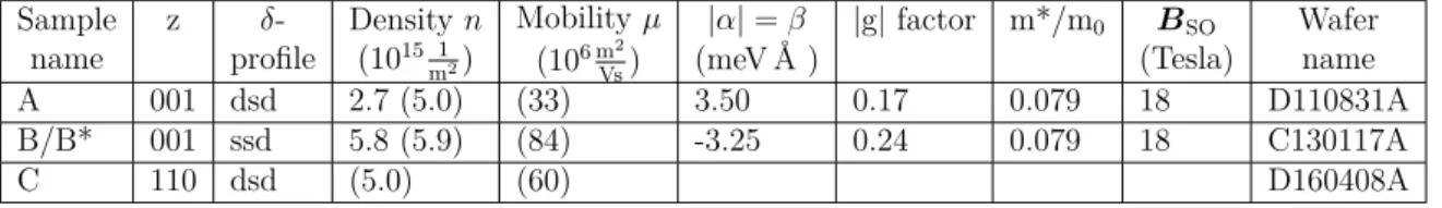
The heterojunction of a single GaAs quantum well embedded in an AlGaAs barrier
is depicted schematically in Fig. 2.3. The relative alignment of the conduction- and
Figure 2.3 | GaAs single quantum well structure embedded in AlGaAs. The alignment of the band edges is described by Anderson’s rule, based on aligning the vacuum levels. Based on [Dav97].
valence band edges (black and blue solid lines) can qualitatively be described by Ander- son’s rule [And62, Dav97]. This rule is based on the electron affinity χ, measuring the required energy to move an electron from the conduction band bottom to the vacuum level (dashed line). The formation of a type I heterostructure, as shown in Fig. 2.3, is the result of Anderson’s rule, stating that the vacuum levels of the involved materials line up. By fabricating a thin layer of GaAs sandwiched between two thick AlGaAs barriers, one obtains a confinement of the electrons perpendicular to the growth direc- tion in the x-y-plane and a quasi two-dimensional electron system is formed. In the simplest scenario, the energy levels of the confined electrons are approximated using the textbook example of an infinitely high potential well. They are described by [Sch04]
E
n,k= E
n,kz+ E
kk= ~
22m
∗nπ d
2+ ~
2k
k22m
∗. (2.1)
Here, n > 0 is the discrete energy subband index, d the width of the quantum well and k
k= (k
x, k
y, 0) the in-plane dispersion of the confined electrons. In Fig. 2.3, the lowest electron subband for n = 1 (solid orange line) is illustrated. As a consequence of the different effective masses m
∗for the heavy- and light hole states in the valence band, a splitting of ∆E
HH,LHat the Γ-point for n = 1 can directly be obtained from Eq. (2.1)
∆E
HH,LH= 1 2
1
m
HH− 1 m
LH~ π d
!
2. (2.2)
The HH and LH valence bands for this case are schematically sketched in Fig. 2.3 as
the two green horizontal lines.
2.2 Sample growth and design
In the course of this work, three different samples with highly specialized properties were investigated. This section starts with a brief introduction into the molecular beam epitaxy (MBE) method, which was used for manufacturing the samples. This is followed by a detailed discussion of the structural composition of each sample, sup- ported by valence- and conduction band potential profile simulations, conducted with the self-consistent Poisson-Schrödinger solver “nextnano++” [Tre06, Bir07]. Also, the application process of an electrical top gate will briefly be discussed.
2.2.1 MBE growth
Figure 2.4 shows the simplified illustration of a molecular beam epitaxy chamber. The
whole system is held under ultra high vacuum (background pressure below 10
−11mbar)
to avoid contamination with impurities and to increase the mean free path of molecules
between collisions to operate in the molecular-flow regime of a gas (also called Knudsen
regime). The furnaces containing the elements to be deposited are called Knudsen cells
(K-cells). They have individual orifices pointing towards the sample holder which are
controlled by mechanical shutters. When a shutter is opened, the evaporated substance
inside a K-cell is forming a molecular beam that enters the MBE chamber and is de-
posited on the substrate layer by layer. For optimal growth conditions, the substrate
is heated and rotated during the deposition. The whole process is monitored, utilizing
RHEED (reflected high-energy electron diffraction), where an electron beam is scat-
tered at the sample surface in grazing geometry. For each fully grown monolayer, the
scattered intensity of the electron beam, displayed on a screen, differs from incomplete
layers, resulting in a periodically changing signal from which the grown layer number
can be measured very precisely.
Shutter Knudsen cell Molecular beam
Electron gun Substrate Heated rotating substrate holder Screen for viewing RHEED
As Ga
Al
Figure 2.4 | Schematic cross section of a MBE chamber in top view. Taken from [Dav97].
2.2.2 Investigated samples
All three samples used in this work are n-doped, 12 nm wide GaAs/AlGaAs quantum wells grown in [001] and [110] crystal direction. A prerequisite of the structural compo- sition was to choose all growth parameters deliberately to obtain a special symmetry of the intrinsic spin-orbit coupling, forming a persistent spin helix regime (see Sec. 2.3.3).
An overview over the important sample parameters is given in Table 2.1.
Sample name
z δ-
profile
Density n (10
15 1m2)
Mobility µ (10
6 mVs2)
|α| = β (meV Å )
|g| factor m*/m
0B
SO(Tesla)
Wafer name
A 001 dsd 2.7 (5.0) (33) 3.50 0.17 0.079 18 D110831A
B/B* 001 ssd 5.8 (5.9) (84) -3.25 0.24 0.079 18 C130117A
C 110 dsd (5.0) (60) D160408A
Table 2.1: Overview of all investigated samples with their most important parameters.
The values in brackets were determined by the manufacturer using magneto-transport mea- surements. All other values were extracted from optical measurements in this work. The abbreviations “dsd” and “ssd” stand for double sided doping and single sided doping.
Sample A
The wafer of this n-doped [001]-grown GaAs-Al
xGa
1−xAs (x = 0.30) sample was man- ufactured at the ETH Zürich under guidance of Prof. Werner Wegscheider in collabo- ration with Gian Salis from IBM-Research Zürich. It was designed to reach balanced strengths of the Bychkov-Rashba (α) and Dresselhaus (β) parameters (see Sec. 2.3).
Since the strength of the linear Bychkov-Rashba coefficient is determined by the built-
in electric field, it was a great challenge to establish the correct doping concentrations
yielding an asymmetric wave function inside the 2DES. One sample piece of this wafer
was used in the experiments of Matthias Walser et al. [Wal12a] where for the first time
a direct mapping of the helical spin state could be shown in time-resolved Kerr rotation
measurements (TRKR). In the work of Christoph Schönhuber et al., another sample
piece of this wafer was used and the spin splitting anisotropy for two different in-plane crystal directions via resonant inelastic light scattering experiments on intrasubband spin-density excitations was first demonstrated [Sch14]. From our spectroscopic data (see Sec. 4.6.1) we could extract the electron density of n = 2.7×10
15m
−2(see Tab. 2.1).
It is lower than the value which was determined in magneto-transport measurements by the manufacturer (n = 5.0 × 10
15m
−2). This deviation could stem from a redis- tribution of electrons from the quantum well to the ionized donors inside the barriers due to laser radiation. Another reason for this quite large difference could be due to fluctuations in the donor distribution, since different pieces of the wafer were used.
The mobility of this sample is µ = 33 × 10
6 mVs2.
A schematic growth pattern of this sample is sketched in Fig. 2.5 (a), where the growth direction (z) points from left to right. The sample hosts a nominally 12 nm-wide single quantum well, located 100 nm below the sample surface and has a so-called inverted doping profile with its dominant Silicon δ-doping layer grown before the quantum well. It is separated by a 20 nm AlGaAs barrier from the quantum well, preventing the ionized donors to act as scatterers in the 2DES region to ensure a high electron mobility. The secondary doping layer was grown for fine tuning of the intrinsic electric field, which is present due to structure inversion asymmetry (see Sec. 2.3.2). The two superlattices located near the GaAs substrate are consisting of thin GaAs/AlGaAs layers, and are designed to prevent impurity atoms from entering the quantum well region during the growth process. An inverted doping profile is not commonly used, because dopants can “float” into the quantum well region during the growth process and act as impurities, reducing the mobility of the 2DES.
Figure 2.5 (b) shows the valence- and conduction band potential profile, simulated with the self-consistent Poisson-Schrödinger solver “nextnano++”. The exact doping con- centrations are unknown, but the ratio between dominant and secondary doping is known to be 5:1, so for the simulation, the total doping concentration amount was var- ied until the simulation output of the electron density matched the optically measured value n = 2.7 × 10
15m
−2(see Table 2.1). At the sample surface, a 5 nm thick GaAs cap layer is grown to prevent oxidation of the AlGaAs barrier. Due to δ modulation doping, a space-charge zone emerges from positively charged Si atomic nuclei leading to a bending of the potential curvature towards lower energies at the two doping regions.
Figure 2.5 (c) is a zoom into the quantum well region of the conduction band with the
squared envelope wave function |χ
0|
2(orange line) of the lowest confined subband level
that can be interpreted as the probability density of electrons. The asymmetric con-
AlGaAs
GaAs QW
AlGaAs GaAs cap
100 nm 5 nm
65 nm
231 nm 25 nm
AlGaAs- barrier 20 nm
AlGaAs- barrier
-500 -400 -300 -200 -100 0
-1.4 -0.7 0.0 0.7
Energy (eV)
Conduction band
Valence band
Si secondary doping Si dominant
doping (a)
(b)
Super- lattice Super- lattice
E
F12 nm 2200 nm
z (nm) Growth direction
z GaAs- substrate
-140 -120 -100 -80 -60 -0.1
0.0 0.1 0.2 0.3 0.4 0.5
Energy (eV)
E
FE-field
Dominant doping
Secondary doping CB 2DES
z (nm) (c)
Figure 2.5 | (a) Schematic growth pattern of sample A (not to scale). The growth direction (z) points from left to right. The different Si-doping concentrations lead to an asymmetric band edge profile. (b) Potential profile of the valence- and conduction band computed with
“nextnano++”. (c) Zoom into the quantum well region of the conduction band potential profile (black solid line) with the probability density of electrons |χ
0|
2(orange line). The green dotted line follows the conduction band potential curvature inside the QW and is sketched for comparison with sample B (see Fig. 2.6 (c)).
centration of the two doping layers leads to the formation of an electric field, pointing
in growth direction (see Fig. 2.5 (c)). Therefore |χ
0|
2has an asymmetric shape with its
maximum inclined to the left side (in direction of the substrate). From the simulations
of Fig. 2.5 (b), we extract a transition energy of E
G∼ 1.5319 eV by measuring the distance between the first quantized states of electrons in the conduction band and heavy holes in the valence band inside the quantum well region.
Sample B
This n-doped, [001]-grown GaAs-Al
xGa
1−xAs (x = 0.33) wafer was fabricated at the University of Regensburg in the group of Prof. Dominique Bougeard. As for sample A, the aim was to achieve balanced Bychkov-Rashba (α) and Dresselhaus (β) strengths.
In contrast, here a single sided doping profile, where the doping layer is grown after the quantum well to reduce incorporation of donor impurities inside the quantum well during the growth process was used. A piece of the same wafer was also used in the work of Markus Schwemmer et al. [Sch16b], where the authors demonstrated the existence of a persistent spin helix state for this sample utilizing time-resolved Kerr rotation measurements. The electron density n = 5.9 × 10
15m
−2and the mobility µ = 84 × 10
6 mVs2were determined by the sample grower. Again there is a deviation for the extracted value from our spectroscopic data n = 5.8 × 10
15m
−2(see Tab. 2.1 and Sec. 4.6.1). The higher mobility compared to sample A is possibly explained by the single-side doping profile: On the one hand, impurities inside the quantum well are minimized due this growth technique as stated before. On the other hand, the electrons are more confined on one side of the quantum well, reducing the scattering on interface imperfections compared to a double-sided doping, where the electrons
“feel” two interfaces [Sch06].
Figure 2.6 (a) illustrates the schematic sample structure with the growth direction pointing to the right side. It has a simplified growth structure, compared to sample A.
The quantum well with a nominal thickness of 12 nm is located 500 nm below the sur- face. Between quantum well and doping layer is a 20 nm AlGaAs barrier. Figure 2.6 (b) sketches the conduction- and valence band profile simulated with “nextnano++”.
A zoom into the quantum well region is shown in Fig. 2.6 (c). Due to the doping layer
on the right side, the intrinsic electric field points to the left hand side (in direction
of the substrate), vice versa as in sample A. This causes the probability density of
electrons |χ
0|
2to be inclined towards the sample surface (orange line). Because the
quantum well is markedly deeper below the sample surface as compared to sample A,
and there is no doping layer between quantum well and substrate, the slope of the
conduction band on both sides of the quantum well is significantly different. On the
substrate side it is nearly horizontal, whereas facing towards the doping layer, it is very
steep. This has a considerable effect on the curvature of the conduction band at the
-800 -700 -600 -500 -400 -300 -200 -100 0 -1.4
-0.7 0.0 0.7
Energy (eV)
Conduction band
Valence band
E
FAlGaAs
GaAs QW
AlGaAs
GaAs- substrate GaAs cap
12 nm
20 nm 460 nm
293 nm 20 nm
AlGaAs- barrier (a)
(b)
Si doping layer
z (nm) Growth direction
z 2038 nm
Super- lattice
-540 -520 -500 -480 -460 -0.1
0.0 0.1 0.2 0.3 0.4 0.5
Energy (eV)
E
FE-field
Doping layer 2DES
CB
z (nm) (c)
Figure 2.6 | (a) Schematic growth pattern of sample B (not to scale). The growth direction (z) points from left to right. Compared to sample A, the simpler design with one-sided doping on the opposite side also leads to an asymmetric band edge profile. (b) Potential profile of the valence- and conduction band computed with “nextnano++”. (c) Zoom into the quantum well region of the conduction band potential profile (black solid line) with the probability density of electrons |χ
0|
2(orange line). The green dotted line follows the conduction band potential curvature inside the QW and is sketched for comparison with sample A (see Fig. 2.5 (c)).
bottom of the quantum well which is quite different for both samples A and B. For
comparison, the curvature of this region for sample A (see Fig. 2.5(c)) was mirrored,
and plugged in Figure 2.6(c) as a green dashed line. This might be an indication that
for sample B there is no homogeneous electric field across the quantum well. From the simulation in Fig. 2.6 (b), we extract a transition energy of E
G∼ 1.5414 eV, which is slightly higher than for sample A, and might originate from the increased band bending of sample B.
Sample B* (gated)
This sample stems from the same wafer as sample B, but was equipped with a semi-
transparent Nickel-Chrome (Ni-Cr) top gate to apply an electric field perpendicular to
the sample surface. The gate was fabricated in cooperation with Johannes Holler and
Dr. Michaela Trottmann at the vapor deposition chamber of Prof. Dominique Bougeard
in the cleanroom of the University of Regensburg. Here, we will give a brief overview
about the top gate fabrication process, a detailed description can be found in previous
publications from our research group [Kug12, Gra17]. Figure 2.7 (a) shows a sectional
view of sample B*. The 2DES is used as a back gate contact. By applying a voltage
between the back- and the top gate, electrons are injected or depleted in the 2DES, de-
pending on the polarity of the voltage. Before the Ni-Cr top gate is applied in the vapor
deposition chamber, the desired top gate position is delimited by applying Scotch
c-
tape to shade the area, where the back gate contacts should be installed, avoiding a
short circuit between top- and back gate. Next, ∼ 15 nm Ni-Cr are deposited in a
vapor deposition chamber. At this thickness, the top gate is semitransparent, and its
transmission ratio is measured to be ∼ 0.5 in transmissivity experiments. To estab-
lish a contact to the 2DES, the top gate free sample surface area, which was shaded
before with Scotch-tape, is scratched with a Tungsten pin and four separated solder
points of Indium are applied and subsequently alloyed at 350
◦C for 60 seconds in a
furnace under forming gas atmosphere. In the last step, the sample is mounted on a
circuit board (see Fig. 2.7 (b)), where the four back gate contacts and two top gate
contacts are bonded with gold wires to larger connection panels to be installed inside
the cryostat.
2DES
Ni-Cr topgate Indium backgate- contact Doping-
layer
U
(a) (b)
Figure 2.7 | (a) Schematic cross section of sample B
∗with Ni-Cr top gate and back gate contacts. (b) Sample B* mounted on the circuit board, attached to the cryostat insert.
Sample C
In the course of this work, an attempt was made to examine the persistent spin he- lix state in grazing-incidence measurements, utilizing resonant inelastic light scatter- ing experiments. Therefore Prof. Wegscheider supplied us with a [110]-grown GaAs- Al
xGa
1−xAs (x = 0.30) sample, hosting a 12-nm wide single quantum well with sym- metric doping profile. With this doping symmetry, no structure inversion asymmetry is present in the 2DES, and the apparent spin-orbit interaction is only due to the Dressel- haus contribution, which points out-of plane for [110]-growth direction (see Sec. 2.3.1).
In this special case, a persistent spin helix (PSH) regime forms for the out-of plane direction (see Sec.2.3.3).
Figure 2.8 (a) sketches the sample structure with the growth direction pointing to the right hand side. The 12 nm wide quantum well is located 230 nm below the surface and is embedded in a 58 nm thick AlGaAs barrier. It is symmetrically doped with three doping layers. The utilized doping technique is called quantum well doping [Uma09], where every Silicon doping layer lies inside a thin, 2 nm wide GaAs single quantum well, surrounded by 1 nm AlAs barrier material. The ratio of the doping concentrations was set by the manufacturer to 80:72:40 (shown in Fig. 2.8 (a) as QW doping 1-3).
The resulting “nextnano++” band edge profile simulation of the conduction band in the quantum well area is shown in Fig. 2.8 (b). Located on the left and right hand side of the 2DES, the spikes in the conduction band stems from the AlAs barrier material of the quantum well doping layers, the Silicon doping is marked as the red dashed lines.
The simulation was conducted in the same way as for sample A and B, by fixing of
the doping concentration ratio for all QW doping layers, until the resulting electron
density was consistent with the specified value n = 5.0 × 10
15m
−2(see Tab. 2.1.) The
-300 -250 -200 -150 0.00
0.35 0.70
Energy (eV)
z (nm) 2DES Si-
doping
E
FAlGaAs
GaAs QW
AlGaAs GaAs cap
231 nm 10 nm
38 nm
58 nm 115 nm
AlGaAs- barrier 58 nm
AlGaAs- barrier 12 nm 800 nm
Growth direction
z GaAs- substrate
22 nm
QW doping 2 QW
doping 3
QW doping 1
AlGaAs
Super- lattice 1 Super- lattice 2
(a)
(b)
Si- doping Conduction
band
Figure 2.8 | (a) Schematic structural composition of sample C (b) Band edge profile simu- lation of the quantum well region of sample C.
orange line shows the probability density |χ
0|
2of electrons inside the quantum well.
Due to the symmetrical slope of the conduction band in the quantum well region, no electric field along the growth direction is present, as it is the case for sample A and B. The extracted transition energy from the simulation is E
G∼ 1.5463 eV.
2.3 Spin-orbit interaction
Spin-orbit (SO) interaction describes the interplay between the spin and orbital de-
grees of freedom of the electrons. The SO interaction originates from a relativistic
description, where a moving electron in an electric field “feels” an effective magnetic
field. The interaction of the spin of the moving electron and this effective magnetic
field is then referred to as spin-orbit interaction. This section will outline the two
main contributions to spin-orbit coupling in GaAs-AlGaAs semiconductor heterojunc-
tions and the resulting lifting of the spin degeneracy in 2DES. The interplay of both
contributions, originating from the bulk inversion asymmetry (BIA) and the structure
inversion asymmetry (SIA), is leading to the formation of a persistent spin helix state,
which will be discussed at the end of this section.
The relativistic interaction between electron spin and orbital angular momentum leads to an additional splitting of the energy bands for |k| > 0. The corresponding spin-orbit interaction Hamiltonian derives from the Dirac equation and is written as [Fab07]
H
SO= − ~
4m
20c
2σ · p × (∇V
0). (2.3) Here, p is the momentum operator of the involved particle, σ is the vector of Pauli matrices and m
0is the free electron mass.
In semiconductor heterostructures, this intuitive picture becomes more complicated, since confinement effects cause band bending, creating an intrinsic electric field (see Sec. 2.2.2). In addition, moving electrons in polar semiconductors such as GaAs are sub- jected to a periodically changing potential, and the effect of this potential on the spin of the electron can be described by a k-dependent magnetic field B
eff(k). Therefore, the symmetry of a semiconductor crystal plays an important role for the description of the spin energy eigenvalues and the spin degeneracy of such a system. For inver- sion symmetric crystals like Silicon, the spin-up (↑) and the spin-down (↓) states are degenerate:
E
↑(k) = E
↓(k), (2.4)
which is a consequence of the combined effect of inversion symmetry in space and time [Kit63]. Space-inversion symmetry changes the wave vector k into −k, resulting in E
↑(k) = E
↑(−k) and time-inversion symmetry, besides changing k, also flips the spin, resulting in E
↑(k) = E
↓(−k), also known as the Kramers relation [Dre55, Fab07].
There are two possible ways to lift this spin degeneracy: On the one hand, the space inversion asymmetry can be broken by internal or external electric fields even in the ab- sence of magnetic fields, where a horizontal splitting of the parabolic subbands emerges.
This is sketched in Fig. 2.9 (a). For materials like GaAs, the space inversion symmetry is already broken due to a lack of crystal inversion symmetry. On the other hand, the time inversion symmetry can be broken by applying an external magnetic field. This leads to a Zeeman splitting [Zee97] of the parabolic subbands, sketched in Fig. 2.9 (b), where a vertical splitting ∆E
Zeemanof the parabolic subbands occurs.
As stated above, the SO-coupling-induced band splitting may be considered as an intrinsic, effective k-dependent magnetic field B
SO(k), and so Eq. (2.3) can be written as
H
SO= ~
2 Ω(k) · σ, (2.5)
Figure 2.9 | The parabolic spin-split subbands of the lowest conduction band are sketched for two cases: (a) Breaking of the space-inversion symmetry is leading to a horizontal subband splitting, where for |k| > 0 the energy splitting ∆E
SOis determined by the strength of the spin-orbit interaction. (b) Breaking of the time-inversion symmetry is leading to a vertical splitting ∆E
Zeemanof the subbands, also known as Zeeman splitting.
with the Larmor precession vector Ω(k) = (gµ
B/ ~ ) B
SO(k).
One usually differentiates between three different space inversion asymmetries: The bulk inversion asymmetry (BIA), the structure inversion asymmetry (SIA) and the natural interface asymmetry (NIA). In GaAs, the impact of NIA is negligibly small, since it originates from heterostructure interfaces in which the adjacent layers share no common atom (e.g. InAs) [Kre96, Win03, Dya08]. For the present work on GaAs, BIA and SIA is essential and will be discussed in more detail below.
2.3.1 Bulk inversion asymmetry - BIA
The lack of inversion symmetry in zinc blende III-V compounds like GaAs (see Sec. 2.1.1), gives rise to a spin splitting of the energy dispersion in bulk materials at zero exter- nal fields. This was theoretically proposed by G. Dresselhaus [Dre55], who derived an expression for the Larmor precession vector from Eq. (2.5) by using general group- theoretical arguments. In the lowest order of perturbation theory, Ω(k) is cubic in k and has the following form
1:
Ω(k)
BIA, bulk= 2γ
~
[k
x(k
2y− k
z2), k
y(k
z2− k
x2), k
z(k
2x− k
2y)]
T. (2.6)
1


![Figure 2.10 | (a) Orientation of the linear Dresselhaus SO field for a 2DES grown in [001]- [001]-direction at the Fermi level (black circle)](https://thumb-eu.123doks.com/thumbv2/1library_info/3726035.1508245/25.892.128.770.432.692/figure-orientation-linear-dresselhaus-field-direction-fermi-circle.webp)