exchange coupling in van der Waals heterostructures
DISSERTATION ZUR ERLANGUNG DES DOKTORGRADES DER NATURWISSENSCHAFTEN (DR. RER. NAT.)
DER UNIVERSITÄT REGENSBURG DER FAKULTÄT FÜR PHYSIK
vorgelegt im Jahr 2020 von
Klaus Zollner
geboren am 31.10.1991 in Bogen
Prüfungsausschuss:
Vorsitzender:Prof. Dr. Vladimir Braun 1. Gutachter:Prof. Dr. Jaroslav Fabian 2. Gutachter:PD Dr. Jonathan Eroms Weiterer Prüfer: Prof. Dr. Andrea Donarini
Termin Promotionskolloquium: 26.01.2021
Two-dimensional materials and their van der Waals heterostructures offer unforeseen po- tential for electronics and spintronics. At present, the available two-dimensional material repertoire covers semiconductors, ferromagnets, superconductors, and topological insula- tors, which already feature highly interesting physics. Remarkably, one can manipulate the properties of a two-dimensional material by proximity effects, while still preserving a great degree of its own autonomy. The ability to control and modify the electronic, spin, and optical properties of two-dimensional materials is extremely valuable for investigating novel physical phenomena, as well as a potential knob for device applications. In this thesis, we investigate graphene, bilayer graphene, and transition-metal dichalcogenides in proximity to various two-dimensional materials. We quantify the spin-orbit and magnetic proximity effects by fitting suitable model Hamiltonians, which capture the relevant low energy elec- tronic and spin properties, to realistic first-principles calculations. As we show, the obtained results can be used for calculating charge and spin transport or optical properties, and are vital for the interpretation of experiments.
Zusammenfassung
Zweidimensionale Materialien und ihre van der Waals Heterostrukturen bieten unvorherge- sehene Möglichkeiten für konventionelle und spin-basierte Elektronik. Momentan ste- hen viele verschiedene zweidimensionale Materialien zur Verfügung, wie zum Beispiel Halbleiter, Ferromagnete, Supraleiter und topologische Isolatoren, welche bereits selbst außerordentliche physikalische Eigenschaften besitzen. Erstaunlicherweise lassen sich diese Eigenschaften von zweidimensionalen Materialen durch sogenannte Näherungseffekte manipulieren. Dadurch, dass man die intrinsischen elektronischen, spin-basierten und optischen Eigenschaften kontrolliert verändern kann, eröffnen sich neue Möglichkeiten für Forschung und Industrie. In dieser Dissertation untersuchen wir Ein- und Zweischicht Graphen, sowie Übergangsmetall-Dichalkogenide, welche durch Näherungseffekte, aus- gehend von verschiedensten anderen zweidimensionalen Materialien, beinflusst werden.
Wir berechnen dafür die Bandstrukturen für eine Reihe von interessanten van der Waals Heterostrukturen mit Hilfe von Dichtefunktionaltheorie. Die Spin-Bahn-Kopplung und magnetischen Näherungseffekte werden näher charakterisiert, indem wir die relevanten En- ergiebänder der Bandstruktur durch geeignete Modelle und passende Parameter beschreiben.
Wir zeigen, dass die daraus resultierenden Modellbeschreibungen verwendet werden kön- nen, um sowohl Spin- und Ladungstransport, als auch optische Eigenschaften zu berechnen, was wiederum essentiell ist, um experimentelle Ergebnisse zu interpretieren.
Part I Motivation and Overview 1
1 Spintronics . . . . 3
2 2D materials and van der Waals heterostructues . . . . 9
Part II Graphene 19 3 The basics of monolayer graphene . . . . 21
3.1 Unit cell, Brillouin zone, and band structure . . . . 21
3.2 Hamiltonian of spin-orbit and exchange proximitized graphene . . . . 23
3.3 Band structure topologies of proximitized graphene . . . . 26
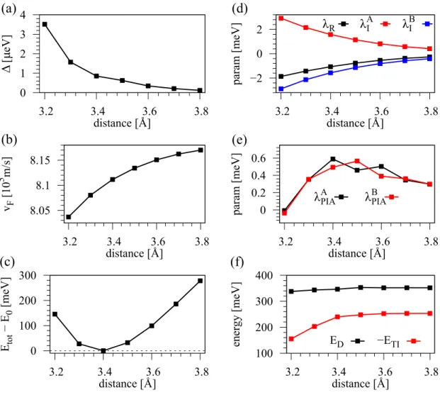
4 Spin relaxation anisotropy in graphene/hBN structures . . . . 29
4.1 Introduction . . . . 29
4.2 Geometry, computational details, and band structure . . . . 31
4.3 Graphene on hBN . . . . 34
4.3.1 Low energy bands . . . . 34
4.3.2 Distance study . . . . 36
4.3.3 Transverse electric field . . . . 38
4.3.4 Spin relaxation anisotropy . . . . 40
4.4 hBN encapsulated graphene . . . . 44
4.4.1 Low energy bands . . . . 44
4.4.2 Transverse electric field . . . . 47
4.4.3 Spin relaxation anisotropy . . . . 48
4.5 Summary and conclusion . . . . 49
5 Proximity spin-orbit coupling in graphene on Bi2Se3 . . . . 51
5.1 Introduction . . . . 51
5.2 Geometry and computational details . . . . 53
5.3 Band structures and fit results . . . . 54
5.4 Transverse electric field . . . . 58
5.5 Distance study . . . . 59
5.6 Different topological insulators . . . . 61
5.7 Summary and conclusion . . . . 62
6 Proximity exchange in graphene on MnPSe3 . . . . 63
6.1 Introduction . . . . 63
6.2 Computational details and geometry . . . . 65
6.3 Band structure and fit results . . . . 66
6.4 Summary and conclusion . . . . 71
Part III Bilayer graphene 73 7 The basics of bilayer graphene . . . . 75
7.1 Unit cell, Brillouin zone, and band structure . . . . 75
7.2 Hamiltonian of spin-orbit and exchange proximitized bilayer graphene . . . . 77
7.3 Band structure topologies of proximitized bilayer graphene . . . . 78
8 Heterostructures of bilayer graphene, WS2, and Cr2Ge2Te6 . . . . 81
8.1 Introduction . . . . 81
8.2 Computational details . . . . 83
8.3 Exchange valve in bilayer graphene on Cr2Ge2Te6 . . . . 83
8.4 Spin-orbit valve in bilayer graphene on WS2 . . . . 88
8.5 Doubly proximitized bilayer graphene . . . . 90
8.6 Summary and conclusion . . . . 94
Part IV Transition-Metal Dichalcogenides 95 9 The basics and strain effects of TMDCs. . . . 97
9.1 Introduction . . . . 97
9.2 Geometry, band structure, and model Hamiltonian . . . . 99
9.3 Strain effects on orbital and spin-orbit properties . . . 103
9.4 Strain tunable optical transitions . . . 106
9.5 Summary and conclusion . . . 108
10 Proximity exchange effects in MoSe2and WSe2on CrI3 . . . . 111
10.1 Introduction . . . 111
10.2 Geometry and computational details . . . 114
10.3 Band structure and twist effects . . . 116
10.4 Short-rangeness of proximity effects . . . 120
10.5 Gate tunable proximity exchange and valley splitting . . . 123
10.6 Summary and conclusion . . . 125
Part V Summary and Outlook 127 11 Recapitulation. . . . 129
12 Novel 2D materials . . . . 133
Part VI Appendix 137
A Supplementary Material. . . . 139
A.1 Supporting Information for chapter 6 . . . 139
A.2 Supporting Information for chapter 8 . . . 140
A.3 Supporting Information for chapter 9 . . . 144
B Employed program packages . . . . 147
Acronyms . . . . 149
References . . . . 151
List of Publications . . . . 179
Acknowledgments . . . . 181
Motivation and Overview
Spintronics
What is spintronics?
Conventional electronics is based on the chargedegree of freedom of the electron. Any information can be encoded into two discrete binary states, 1 and 0, represented by a finite or absent flow of charge in an electronic circuit. In contrast, modern spintronics [1–4] is based on another degree of freedom of the electron:the spin. The two degrees of freedom, charge and spin of the electron, are linked and cannot be directly decoupled from each other. Imagine the electron as a tiny charged sphere that can rotate either clockwise or counter-clockwise around its own axis, while moving in the Coulomb field of the atomic nuclei. This intrinsic rotational sense of the electron is called spin, which can be eitherupor downwith respect to the chosen quantization axis, usually thezone. Similarly, the earth is rotating around its own axis while moving in the gravitational field of the sun. However, spinis of purely quantum mechanical nature, while the rotating earth can be described by classical physics. Binary data, 1 and 0, can now be encoded in those two spin states, up and down, similarly to the presence or absence of charge in electronics. We can measure the spin, because it is associated with a magnetic moment of a rotating charge. Some materials, such as cobalt, nickel, and iron are magnetic, because enough electron spins are aligned (rotate in the same direction), generating a global magnetization.
The field of spintronics rooted in the early 1920s, when O. Stern and W. Gerlach first demonstrated the quantization of the atomic magnetic moment in a magnetic field [5].
Only a few years later, W. Pauli formulated the quantum mechanical description of the electron’s spin with the help of simple matrices [6]. When people then started to study spin-polarized transport, they found out that electrons of majority and minority spin flow rather independently in a ferromagnet [7, 8], and charge currents can be spin-polarized.
A major role in the understanding of spin-polarized transport is attributed to tunneling experiments through metal/ferromagnetic insulator (FMI)/metal junctions [9]. An unpo- larized current can become spin-polarized when passing through the FMI tunnel layer, as proven by the magnetic field dependence of the current-voltage characteristics [10–12].
Experimentalists also studied ferromagnet/insulator/superconductor [13,14] and ferromag- net/insulator/ferromagnet junctions, and M. Julliére was able to derive a formula for the tunneling magnetoresitance (TMR), which depends on the spin polarization of the ferro-
magnets [15]. In a ferromagnet/insulator/ferromagnet junction, the relative direction of the two magnetizations affects tunneling, founding the basis of the spin-valve effect, see Fig. 1.1. A subsequent major discovery, that was awarded with the Nobel Prize [16] and revolutionized hard disk technology, is the giant magnetoresitance (GMR) effect [17–19]. In ferromagnet/metal/ferromagnet junctions, parallel and antiparallel aligned ferromagnets lead to significantly different resistances when passing a current through the junction. For TMR and GMR, the magnetization switching of the ferromagnet is therefore essential to control the flow of spin-polarized currents. Also the reverse process is possible: a spin- polarized current can switch the magnetization of a ferromagnet, due to transfer of angular momentum. This effect is known as the spin-transfer torque (STT) [20].
FerromagnetInsulatorFerromagnet
B
z0
R
pR
apz x
M1 M2
Figure 1.1:Left: Schematic structure employed for the TMR effect, consisting of two ferro- magnetic layers separated by an insulating tunnel barrier. The magnetizations M1andM2 of the two ferromagnets are aligned parallel, but can be switched with an external magnetic fieldBz along thezaxis. Right: The tunneling resistance as function of the magnetic field Bz(red = up-sweep, blue = down-sweep), when current is injected along thexaxis across the ferromagnet/insulator/ferromagnet junction. For parallel M1 and M2, the junction resistance is low (Rp), while for antiparallel alignment, the resistance is high (Rap), due to spin-dependent electron tunneling and scattering. The relative resistance change is given by (Rap−Rp)/Rpand defines the efficiency of the TMR effect.
Applications and challenges of spintronics
In electronic devices, e. g., personal computers, millions of transistors are responsible for logic operations, which require special semiconducting materials that control the charge flow. In spintronics, we actually do not need these specially designed materials, as spin can be measured by common ferromagnets and metals. People also argue that the power consumption is much lower in spintronics [21]. By applying electric fields, the magnetization, or equivalently the spin polarization can be changed quite easily, while in electronics a lot of power is consumed by maintaining the charge flow. Additionally, the switching rates for spin states are very high. Becausespinis an intrinsic property of the electron and not energy dependent, spins can in principle maintain their direction, even after shutdown of the power source. Especially this last property is important for the design of novel nonvolatile
memory devices, where the information could be practically stored forever without power consumption. However, these considerations are very idealistic. For example, spins will always interact with their surroundings, especially in solid media, such that scattering leads to the loss of the spin information. In addition, the amount of energy to generate and maintain the spin dependent properties of a device might overcome the low power consumption needed for the actual spin operations. Moreover, to master the mentioned obstacles for spintronics, we are also bound to special materials and novel device designs.
Is spintronics ready for the mass market industry? Certainly, the answer is Yes! In 2007, when A. Fert and P. Grünberg received the Nobel Prize for the GMR effect [16], their discovery had entered industry for about 10 years. In 1997, IBM was the first company to implement GMR structures in hard disk read heads [22]. By employing the GMR effect, storage densities were drastically increased, while simultaneously decreasing resistance and thus speeding up the reading and writing processes. The key ingredient for the GMR effect is a ferromagnet/metal/ferromagnet junction. One of these ferromagnets can easily switch its magnetization direction (soft ferromagnet), while the magnetization direction of the other ferromagnet is practically fixed (hard ferromagnet). The bits are stored in magnetic units on rotating disks. When the read head is above a magnetic unit of the disk, the soft ferromagnet adapts its magnetization direction. Whenever the soft ferromagnet switches its magnetization direction, the junction resistance of the read head will drastically change, which can be measured by passing a current across the junction. Similar things hold for the TMR effect, where the metal layer is replaced by a tunneling barrier, see Fig. 1.1. Microscopically, electrons with their spin parallel to the magnetization of the ferromagnet will experience less scattering than electrons with antiparallel spin, leading to giant magnetization dependent differences in resistance. Of course, the efficiency of the GMR effect is a matter of device engineering and the search for optimal material combinations with appropriate thicknesses. The current generation of data storage solutions are based on this magnetic random access memory (MRAM) technology, which employs even more advanced spin-based phenomena, such as the TMR effect, STT, and spin-orbit torque (SOT), leading to even smaller devices with giant storage densities and ultrafast information processing [23].
At this point, two-dimensional (2D) materials enter the game, which are promising for pushing this field to the ultimate limits, regarding size and efficiency.
Despite these very general advantages and first applications, there are also some chal- lenges. The main goal in spintronics is to transport information, represented by the spin of the electron, while optimally no net charge current flows in the transport channel. In order to do so, we need to efficiently generate, inject, on-demand manipulate, and detect the spin information. The injection of spins can be achieved electrically by conventional ferromagnet/insulator tunnel junctions, where the conductivity mismatch plays a major role [24]. Another possibility is the hot-electron spin injection [25] method, which circum- vents conductivity mismatch. Spins can be also injected optically in semiconductors [26], employing the difference in the absorption of left- and right-handed circularly polarized light and the special optical selection rules. More advanced spin injection methods are
based on spin pumping, driven by magnetization dynamics [27], or by current-induced spin orientation via spin Hall effect (SHE) and spin-orbit interaction [28]. The detection of the spin information is typically just the inverse of one of the injection processes.
Once the spins are injected into the desired material, we need to transport the information that they carry. There are several mechanisms that can influence the spin information and lead to a temporal evolution of the spin density [3], according to
∂s
∂t =−vd∇s+D∇2s+s×ω0− s
τs. (1.1)
The four terms correspond to spin drift, diffusion, precession, and relaxation. The final spin densitys(r,t)depends then on the initial spin densitys0(r), the spin diffusivityDof the system, the drift velocityvddue to an applied electric field, the precession frequencyω0 due to an applied magnetic field, and the spin relaxation (SR) via a characteristic lifetimeτs. As we can see, there are a lot of external influences on the spin density, which are strongly determined by the actual materials that are used. For example, the drift velocity depends on the electron mobility and the actual band structure. The relaxation rate depends on the impurity and doping density, temperature, spin-orbit coupling (SOC), etc. Of course, the individual parameters also mutually influence each other. In the end, everything boils down to find the most adequate material combinations and the optimal settings, suitable to achieve the desired spin transport qualities, while simultaneously maintaining an efficient way to control the spin information. However, this is a highly nontrivial task and a lot of efforts are necessary to bridge the gap between the basic idea and final mass market devices.
(a) (b)
Figure 1.2:Schematics of the Datta-Das spin field-effect transistor (FET) [29]. Source and drain ferromagnetic contacts with parallel magnetizations are used to inject and detect the spins (small arrows). The transport in the 2D electron gas channel depends on the precession of the electron spins, which is due to SOC, i. e., an effective magnetic field. The SOC in the channel can be manipulated with a gate voltageVg. (a) In the ON state, when there is no gate voltage applied, spins experience no precession and keep their original alignment. The current is large. (b) In the OFF state, spins precess and have opposite alignment compared to the ferromagnetic drain contact. The current is small. Figures are from Ref. [30].
A particular example of this is the still elusive Datta-Das spin FET, shown in Fig. 1.2, which has been proposed 30 years ago [29]. The basic idea is to inject spin polarized electrons from the ferromagnetic source contact into a, for example, 2D electron gas formed at a GaAs/AlGaAs interface. The electrons flow ballistically along the transport channel and arrive at the ferromagnetic drain contact. Depending on the orientation of the electron spin with respect to the drain contact magnetization, they can either enter the contact or not, i. e., current flows or not. The gate voltageVgis responsible for generating an effective magnetic field in the transport channel, which is due to SOC and leads to precession of the spins.
Depending on the gate voltage, precession and consequently the current flow can be turned on and off.
The current generation of spintronics devices employs hybrid geometries consisting of several ultrathin 2D materials in order to overcome intrinsic limitations of the transport medium via proximity effects. For example, the previously introduced concept of the spin FET can be potentially realized in a bilayer graphene (BLG)/transition-metal dichalcogenide (TMDC) heterostructure [31]. In addition, TMR structures have been investigated, which exclusively consist of 2D materials and show giant efficiencies [32]. As a result, a new branch of condensed matter physics has emerged, which is solely dedicated to the interface and band structure engineering of 2D layers. In this context, also new subfields such as straintronics, valleytronics, and optospintronics have emerged, where additional control possibilities and degrees of freedom enter the game. The ability to precisely control and modify the electronic, spin, and optical properties of materials would be extremely valuable for investigating novel physical phenomena, as well as a potential knob for device applications. In this thesis, we consider several such 2D material heterostructures and analyze the proximity effects, always with regard to possible spintronics applications. In the next chapter, we will first introduce 2D materials and van der Waals (vdW) heterostructures, and summarize some application prospects.
2D materials and van der Waals heterostructues
What are 2D materials?
In solid state theory, one typically deals with crystals that have finite extensions along all three spatial directions. Such materials, where the electronic motion is unconfined within the crystal, is called three-dimensional (3D) or commonly termedbulk. Even if the material is only a micrometer in size, we still call it a bulk crystal because the spatial extensions along all directionsxiof the crystal are much larger than the thermal de Broglie wavelength λ=
q
2πh¯2/mkBTof the electron (λ≈4.3 nm forT=300 K). Consequently, electrons will effectively not feel the surface boundary of such a bulk crystal. Conversely, this means that if the motion of the electron is spatially confined, we talk aboutquantum confinementand new physical phenomena can appear [33]. A very general classification of crystals can be done via their dimensionality.
If we confine the electronic motion within a layer with thicknessd <λ, for example by thinning down a material, we get a two-dimensional (2D) system. A typical example for quantum confinement in 2D is a AlGaAs/GaAs/AlGaAs heterostructure. If the central GaAs region is thin enough, we speak of aquantum well, where the electronic and optical properties can be strongly altered compared to the bulk GaAs crystal. In this scenario, the confinement is due to the potential well that forms in the GaAs layer because of the surrounding AlGaAs layers. Similarly, one can apply confinement along two spatial dimensions and we end up with a one-dimensional system, a so-calledquantum wire. It is even possible to confine electrons in all three spatial dimensions and the system is then zero-dimensional. Such a zero-dimensional system is called quantum dot, which can be regarded as an artificial atom with discrete energy levels. Nowadays, when we speak of 2D materials, we actually mean true monolayers of a crystal. Their bulk materials are formed by individual ultrathin layers that are held together by weak van der Waals (vdW) forces. These monolayers have interesting physical properties and can even be combined in a lego-like fashion in vdW heterostructures [34].
The most prominent and prototypical example of a 2D material is graphene. It is a single layer of carbon atoms that are arranged in a honeycomb lattice [35,36]. Consequently, it is the ultimate limit that can be reached for quantum confinement because the thickness of graphene equals the size of an atom. Remarkably, graphene displays extraordinary
properties [37,38], such as giant mobility, mechanical robustness, optical transparency, and much more. Therefore, it is applicable in several devices in diverse fields, such as chemical sensors [39] and flexible electronics [40]. If we replace the carbon atoms in graphene by boron and nitrogen atoms, we get its insulating “analog” hexagonal boron nitride (hBN) [38].
hBN is a wide band gap insulator and, due to its chemical inertness, it is frequently used as encapsulation material for other 2D materials to protect them from the environment and degradation [41].
Figure 2.1:Examples of a few different and important 2D vdW crystals with diverse proper- ties. For each material, we show the structure of a “monolayer”.
A huge class of 2D materials are transition-metal dichalcogenides (TMDCs) [42]. Bulk TMDCs are layered vdW crystals, where each monolayer is formed by a layer of transition- metal atoms surrounded by top and bottom layers of chalcogen atoms. Interestingly, several different polytypes of TMDCs exist, such as the 2H, 1T, and 1T0 forms, that only differ by the relative arrangement of transition-metal and chalcogen atoms in the unit cell, which can have drastic consequences for electronic properties. For example, the bulk 2H-form of MoS2
is an indirect band gap semiconductor, while a monolayer has a direct band gap in the visible optical range [43,44]. In contrast, the 1T-form of, for example, TaS2is a metal and can exhibit a series of rather exotic electronic states, including superconductivity or a charge density wave (CDW) phase [45]. Even though TMDCs are experimentally known since about the 1920s [46], the monolayers have been prepared and properly characterized just recently, as in the case of MoS2[43]. Especially the semiconducting TMDCs are technologically important building blocks for spintronics, optics, and transistors [47–49].
Another important class of 2D materials are the magnetic ones [50–53], which are indis- pensable for devices that require magnetism, such as the giant magnetoresitance (GMR) and tunneling magnetoresitance (TMR) effects. Examples of vdW layered magnetic crystals are the transition-metal trihalides (TMTHs) CrI3and CrBr3, as well as transition-metal trichalco- genides (TMTCs), such as Cr2Ge2Te6(CGT), in which ferromagnetic order is present in the monolayer limit [51,52]. For a long time, people believed that long-range magnetic order could not be present in a 2D system [54]. However, since these materials have perpendicular magnetic anisotropy (PMA), ferromagnetic order is stabilized even for the monolayers. Simi- larly to the TMDCs, the vdW magnets are known to physicists for quite some time, but just recently monolayers were successfully fabricated and characterized [55]. A drawback for applications is the reduced Curie temperature of the monolayers compared to their bulk counterparts, which is already well below room temperature [51]. Another issue is the stability of these magnetic materials under ambient conditions [50], an obstacle that can be overcome by the encapsulation with hBN.
Above are just a few examples of 2D materials with diverse properties. Fortunately, for every 3D material class, we now have at least one 2D analog available, be it metal, insulator, superconductor, ferromagnet, antiferromagnet, semiconductor, or topological insulator. In Fig. 2.1, we summarize a few very important representatives of 2D crystals, which offer unforeseen opportunities, but also challenges, to electronics, spintronics, optics, and magnetism.
How to create a 2D material?
The creation of a 2D material is a delicate task and a lot of efforts are needed to achieve large scale and high purity samples, which are the ultimate requirement for mass market applications. In general, two different approaches can be distinguished: 1) separation of individual monolayers from the bulk compound and 2) direct growth of the monolayer material via assembling the atomic constituents.
The first technique is, from a theoretical point of view, a very simple one. Take a piece of sticky tape and apply it to the material of interest, provided that it is a vdW layered crystal.
Eventually, one will peel off a monolayer of the vdW crystal, which is sticking to the tape.
The tape will then be pressed on a suitable substrate, such that the peeled off monolayer will be transferred from the tape to the substrate. This process is called mechanical exfoliation or Scotch-tape method [56]. Typically, the peel off process is repeated many times to enhance the probability for monolayer generation, before the tape is pressed on the substrate. Subsequent scanning of the substrate via an optical microscope is often used to search for regions where a monolayer is present. The advantage of this method is that no chemical reactants are present during the exfoliation process, which could degrade the sample quality. However, one has no direct control of monolayer generation and the sample sizes are usually small.
This technique, which is still frequently used, was the first one to peel off graphene layers from the graphite crystal [57], which initialized the whole field of 2D material research.
Another technique to separate the monolayers from each other is the liquid exfoliation method [58–60], where several fine tuning options exist. The basic idea is to suspend the vdW material, typically in powder form, in a special liquid solvent. Among sonication of the liquid mixture, microbubbles are created and annihilated due to the pressure pulsations.
The bubble cavitation lead to shock waves which provide the normal and shear forces that act on the vdW material, separating the layers from each other. The success of monolayer generation strongly depends on the sonication power, but primarily on the solvent that is used to efficiently overcome the vdW forces between the layers. The exfoliated flakes can be extracted via filtration or drop casing, typically including some residuals from the exfoliation process, which is just one drawback of this method. In addition, the monolayer yield is usually low and the flake sizes are small, having also high defect densities.
One of the most frequently used growth techniques for large scale production of 2D materials is the chemical vapour deposition (CVD) [61–63]. For the CVD growth process, some precursor materials are necessary, which already contain the atomic constituents of the desired monolayer material. In the case of graphene, typically a mixture of CH4/H2 gas is used, for which the flow rate can be easily controlled. For TMDCs, metal oxides or foils in combination with sulfur or selenium powders are heated to create the gasified solid precursors. These precursor gases are lead into a heated furnace, where they react with each other such that the desired 2D material will grow on a suitable substrate. The substrate itself can have an additional catalytic functionality to improve the overall growth success. Especially for the CVD growth process, it is vital to stick to specific guidelines, concerning temperature, gas pressure, and time duration, to get high quality monolayer samples [61]. Remarkably, under well-controlled growth conditions, many features, such as grain sizes, number of layers, the orientation, or crystal phase (especially important for TMDCs), can be precisely tuned. It is even possible to grow vdW heterostructures with CVD- based techniques. Already in 2010, macroscopic graphene films were grown on Cu-foils [64], showing the indispensable role of CVD for the mass market production of 2D monolayers.
Another technique to create 2D materials is the molecular beam epitaxy (MBE) [65], which is one of the most important methods for industry, as it allows to easily grow clean semiconductor heterostructures with sharp interfaces. The MBE growth process takes place in an ultrahigh vacuum chamber to reduce impurities from residual atmospheric gases. Effusion cells, containing the pure atomic constituents, are heated such that directed molecular beams can be shot on a substrate within the chamber. The whole growth process can be monitored in situ with the help of the reflection high-energy electron diffraction (RHEED) technique. Several control knobs, such as temperature and substrate material, decide on the overall growth process, quality, and resulting deposited crystal. MBE holds promise for continuous and scalable growth, especially for TMDC mono- and multilayers [66–
68], but also for graphene [69] and hBN [70].
The mentioned creation techniques are briefly summarized in Fig. 2.2. For industrial purposes, it is incredibly important to grow 2D materials in a large scale, cheap, and repro- ducible way. Remarkably, since the first mechanical exfoliation of graphene, researchers made a great progress towards realizing this, especially by customizing CVD and MBE for the growth of monolayers.
Figure 2.2:Creation techniques for 2D materials. (a) Micromechanical exfoliation with the help of an adhesive tape and subsequent transfer on a substrate. (b) Liquid exfoliation method, where graphite powder is placed in a liquid solution and among sonication the mono- and multilayer flakes are created. (c) Powder-based CVD method, where a carrier gas transports the source powders to the substrate within a heated quartz tube. (d) MBE method, where directed molecular beams from effusion cells are shot on a substate. Figure (a) from Ref. [71], (b) from Ref. [72], and (c,d) from Ref. [73].
Application prospects of 2D materials and their heterostructures
For field-effect transistor (FET) device applications, operating at high frequencies, it is important that the channel material has a large carrier mobility [74]. Conventional bulk semiconductors (Si, Ge) have mobilites typically ranging in between 102–104cm2/Vs, while III-V compounds (InAs, InSb) can even reach up to 105 cm2/Vs [75,76]. In contrast, 2D monolayer graphene flakes, grown by CVD on copper and encapsulated in hBN, show mobilities of around 106 cm2/Vs [77]. Recent experiments could even demonstrate that graphene in a vdW heterostructure with a TMDC can have a giant room temperature mobility as high as 350.000 cm2/Vs [78], well above the predicted limits due to acoustic phonons [79].
Graphene-based FETs begin now to outperform Si-based technology [80–82]. Moreover, charge carriers in graphene are ultra-sensitive to external influences, such as adatoms and
admolecules that are attached to it. Even single molecule absorption can be detected, due to relatively large changes in graphene’s resistivity [39]. Thus, graphene can be used as a powerful detector for poisonous gases.
Nevertheless, for transistor applications, semiconducting materials with a band gap are advantageous to semimetallic graphene. One such 2D material is phosphorene, which shows good ambipolar device performance with relatively high mobilities and on/off ratios [83,84].
In addition, the anisotropic transport, optical, and mechanical properties of phosphorene, which originate from its puckered crystal structure, could be relevant for novel flexible device designs [85], see Fig. 2.3(d). Furthermore, phosphorene shows a layer dependent band gap ranging from 0.3 eV (bulk) to 2 eV (monolayer), thus bridging the gap between near-infrared and the visible spectrum. Phosphorene is also a superior thermoelectric material and can be used in photodetectors with similar response times as graphene [83,86]. Recent studies also demonstrate that phosphorene-based heterostructures are suitable candidates as water splitting photocatalysts [87].
Also TMDCs are semiconductors, with band gaps in the visible spectrum, that can be used for ambipolar FET device applications, which are highly efficient when an electric double layer (ionic liquid) is used as gate dielectric [42,48,91]. One pecularity of TMDCs is the spin-valley locking, the helicity selective optical excitation of carriers with certain spin in a certain valley1 at the same excitation energy. The spin-valley locking provides another degree of protection for charge carriers, important for information technology. In particular, it is a very attractive property for the field of valleytronics [92], for example as a spin and valley-polarized current source. Another possible application area for TMDCs is in photonics devices [48,93,94], as they are highly sensitive to polarized light and can be used in photodetectors and light emitting devices with controllable emission helicity.
The recently discovered magnetic materials, such as CGT and CrI3 are long-awaited building blocks in spintronics for nonvolatile magnetic random access memory (MRAM) technology [50–52,95]. For example, magnetic tunnel junctions consisting of CrI3[90,96], showing giant magnetoresistance ratios up to 10.000%, are ideally suited for novel TMR devices, see Fig. 2.3(c). Furthermore, the distinct resistance states can be controlled and tuned fully electrically by gating and doping in multilayer CrI3structures. Unfortunately, the operation is limited to low temperatures due to the Curie temperature of the currently known 2D magnetic materials.
Heterostructures formed by 2D materials are also very attractive from another point of view, since we can easily stack them in a lego-like fashion so that proximity effects can play an important role. The first demonstration of proximity-induced phenomena dates back to 1932 in normal-metal/superconductor junctions, where superconductivity “leaks” into the normal-metal [97]. Similarly, combining a strong spin-orbit coupling (SOC)2or magnetic material, with a generic 2D crystal layer, one can induce spin-orbit or exchange coupling
1The term “valley” denotes a local minimimum/maximum in the conduction band (CB)/valence band (VB) of the band structure. For the direct band gap semiconducting monolayer TMDCs, the valleys are located at the K and K0points of the Brillouin zone (BZ).
2A strong SOC material would be for example a TMDC or a topological insulator (TI), where the characteristic band structure features are dominated by SOC.
Figure 2.3:Device schemes employing 2D materials and their heterostructures. (a) Opti- cal spin injection into graphene with the help of a semiconducting TMDC. The circularly polarized light generates spin-polarized electrons in the TMDC, which are transferred to graphene and subsequently detected as a Hanle signal by the ferromagnetic electrode.
(b) Sketch of the geometry to measure the proximity-induced inverse spin Hall effect (SHE) in graphene/TMDC heterostructures. The precession of the spins and the spin-to-charge con- version is sketched. (c) Schematics of a spin tunnel FET based on a gate-tunable ferromagnet- to-antiferromagnet transition in bilayer CrI3 and the spin filtering in the tunnel junction.
Arrows indicate the magnetization in each CrI3layer. The left and right panels correspond to a low and a high tunnel conductance state, respectively. (d) Illustration of the device structure of a flexible back-gated black phosphorus FET on a polyimide substrate. Even after 5.000 bending cycles, the device performance did not degrade. Figure (a) from Ref. [88], (b) from Ref. [89], (c) from Ref. [90], and (d) from Ref. [85].
by the proximity effect [30]. Therefore, one can effectively add multiple spin interactions to a 2D material which intrinsically lacks superconductivity, strong spin-orbit, or magnetic exchange coupling. Nowadays, vdW heterostructures are considered for proximity effects, exclusively consisting of 2D crystal layers. In fact, proximity effects offer new opportunities in condensed matter physics. On the one hand, different materials can mutually benefit from each other and allows for the efficient manipulation of electronic and spin properties. On the other hand, proximity effects in 2D vdW materials typically leave the characteristic intrinsic properties of the individual materials intact.
Figure 2.4: (a) Schematic view of a CrI3/TaSe2 vdW heterostructure consisting of an insulating antiferromagnetic bilayer-CrI3 and a nonmagnetic metallic monolayer TaSe2. The spin-orbit torque (SOT) switches the magnetizationm1 to get an antiferromagnet-to- ferromagnet reversible phase transition. (b) A read-out current Ireadcan be used to probe the TMR(θ) = [R(θ)−R(0)]/R(0)of the heterostructure, as function of the angleθbetween magnetizationsm1andm2on two monolayers of CrI3. Here,Rdenotes the resistance of the junction. Figures are from Ref. [98].
For example, highly discussed material combinations are graphene/TMDC heterostruc- tures. Graphene lacks a band gap, has very low optical absorption, nearly no intrinsic SOC, but excellent electronic and spin transport properties. In contrast, TMDCs display excellent optical absorption in the visible range with spin-valley locking, but with poor mobilities. In addition, TMDCs have strong intrinsic SOC. Consequently, graphene/TMDC heterostruc- tures are very well suited for optospintronics devices, where spin polarization is optically generated in the TMDC and subsequently transferred to graphene [88,99], see Fig. 2.3(a).
Recent experiments have focused also on the proximity-induced SOC in graphene, due to the nearby TMDC, which causes a giant lifetime anisotropy in graphene’s spin transport [100].
Remarkably, the intrinsic SOC of graphene can be enhanced by two orders of magnitude, by the proximity effect, while still preserving the characteristic Dirac dispersion. Moreover, interconversion between spin and charge currents in graphene/TMDC heterostructures can be achieved via SHE, see Fig. 2.3(b), and Rashba-Edelstein effect (REE) [89,101–103].
The conversion can be tuned in sign and magnitude by gating, which offers a route for fully electrical spin generation and manipulation, without further need of ferromagnetic electrodes.
One particular example of an all 2D material vdW heterostructure, especially interesting for novel SOT-based MRAM technologies, is shown in Fig. 2.4(a). In the CrI3/TaSe2vdW heterostructure, consisting of an insulating antiferromagnetic bilayer-CrI3and a nonmagnetic metallic monolayer TaSe2, an antiferromagnet-to-ferromagnet reversible phase transition can be induced by SOT [98]. The unpolarized charge current is injected parallel to the interface by a small applied bias voltage Vbbetween the left and right electrodes. The charge current in the strong SOC TaSe2layer, leads to a transverse spin current across the CrI3/TaSe2interface.
Due to SOT, a reversible switching of the magnetizationm1 of the lower CrI3 layer can be achieved, by passing short current pulses. A transverse read-out current Iread can be used to probe the TMR ratio of the heterostructure, as function of the angleθbetween the magnetizationsm1 andm2 of the two monolayers of CrI3, see Fig. 2.4(b). By employing suitable graphene/hBN tunneling electrodes, the magnetic states of the bilayer-CrI3can be well distinguished, with a maximum TMR ratio of about 240%.
Another example for applications of vdW heterostructures are TMDC-based p-n junctions as high performance photodetectors [104–106]. By combining two different TMDC layers in a heterobilayer, very efficient charge separation is possible. Depending on the combined TMDC monolayers, a special type-II band alignment is achieved, where the conduction band (CB) is formed by one layer, while the valence band (VB) is formed by the other TMDC layer, such that electrons and holes are located in different layers. The resulting photodetectors can operate with zero bias voltage, due to the built-in field of the heterostructure. Furthermore, they show fast response times, high on/off ratios, and wide wavelength detection ranges.
The mentioned application prospects give just an initial impression of what is possible with 2D materials and heterostructures. We are not yet at a stage, where these new 2D-based device developments can drastically outperform the conventional state-of-the-art technology.
Nevertheless, 2D materials and their heterostructures offer a rich playground for basic research, and hold promise for novel devices in diverse fields. In the following chapters, we will show our results on proximity effects in 2D material heterostructures and discuss their significance for research and industry.
More specifically, in the next part we will talk about graphene-based structures. After introducing a low energy model Hamiltonian, suitable to describe the proximity-modified Dirac states of graphene, we first focus on graphene/hBN heterostructures. Based on ex- tensive density functional theory (DFT) calculations, we find that graphene’s characteristic dispersion is preserved with additional weak proximity SOC in theµeV regime. Subsequent spin lifetime and spin relaxation (SR) anisotropy calculations allow us to discuss the signifi-
cance of these structures for charge and spin transport experiments. In particular, we will see that spin lifetimes are on the order of few to tens of nanoseconds, while SR anisotropies are gate tunable and can reach giant values. Next, we discuss the proximity SOC in graphene/TI heterostructures. In great contrast to hBN, the TI induces a much larger SOC in graphene on the order of few meV. The magnitude of the induced SOC depends on an external gate voltage, the atomic constituents of the TI, and the interlayer distance, which are tuning knobs to find ideal experimental conditions for, e. g., spin-to-charge conversion efficiencies in graphene/TI stacks. In the last chapter about graphene, we discuss the proximity-induced exchange coupling due to the Ising antiferromagnet MnPSe3. Surprisingly, antiferromagnetic exchange is induced in graphene, i. e., the effective couplings in the model have opposite sign for the different sublattices in order to fit the DFT dispersion. This behavior has never been reported before and opens new avenues for the design of topologically protected edge states in graphene.
In Ch. 7, we switch gears and introduce the basic properties of bilayer graphene (BLG).
Especially its unique gate tunable low energy dispersion, with sublattice- and layer-polarized bands, is important for exotic device concepts where spin interactions can be turned on and off. In particular, we will discuss multiple heterostructures comprising BLG, semiconducting TMDCs, and the ferromagnetic insulator (FMI) CGT. Due to the short-range proximity effects, only adjacent layers influence each other. Consequently, spin-orbit and exchange couplings can be fully electrically turned on and off or swapped in the conduction electrons of BLG. Our results provide a basis for unique multifunctional device architectures, employing the full potential of vdW heterostructures and related proximity-induced phenomena.
In the last part of this thesis, we will discuss TMDCs. One important key ingredient for flexible electronics are 2D materials because of their mechanical strength. In this con- text, especially the semiconducting TMDCs are attractive and this is why we study their strain tunable band structures and optical properties in Ch. 9. Even though these results are not directly related to proximity effects, they are still vital for the interpretation of experiments and heterostructure DFT calculations. In the last main chapter, we consider TMDC/(hBN/CrI3)/CrI3structures. The proximity-induced exchange coupling is short- ranged and originates from the adjacent magnetic CrI3layer only. The induced magnetism, combined with the giant intrinsic SOC of the TMDCs, breaks the valley degeneracy in the dis- persion. The relevant TMDC band edges at the K and K0points experience a valley splitting on the order of a few meV, which can be tuned by gating and twisting the TMDC/CrI3het- erostructures. Technologically, this offers a way for persistent valley polarization in TMDCs, and the valley degree-of-freedom could be employed in novel valleytronics heterostructure devices.
Graphene
The basics of monolayer graphene
In this chapter, we introduce the basic properties of monolayer graphene, such as unit cell, band structure, and low energy Hamiltonian. The Hamiltonian is based on effective pz orbitals of graphene that can be modified by proximity effects. The modification of the Dirac bands due to proximity of graphene to other materials, such as monolayer transition- metal dichalcogenides (TMDCs) or ferromagnets, can be described by a series of parameters, including orbital, spin-orbit, and exchange effects. The parameters can be determined by fitting the Hamiltonian to a first-principles calculated band structure of a graphene- based heterostructure system. Finally, we briefly analyze the impact of proximity spin-orbit and exchange coupling on the low energy band structure by employing realistic model parameters according to density functional theory (DFT)-calculation examples.
3.1 Unit cell, Brillouin zone, and band structure
The element carbon is very important, especially for life on earth, since all living (organic) compounds contain it. Due to the special electronic configuration [He] 2s22p2, with 4 valence electrons, it has the ability to form complex molecules and shows the greatest diversity of chemical combinations among all elements. For example, carbon is found in complex hydrocarbon chains, such as in fossil fuels and plastics which are essential for industry. In great contrast, diamond, one of the hardest and most precious crystals on earth, is also formed by carbon atoms.
A highly discussed material, which exclusively consists of carbon atoms, is graphene.
Its prominent properties, like giant electron mobility, optical transparency, and mechanical robustness [77, 107–109], make it very appealing for research, especially in the fields of electronics and spintronics. Monolayers of graphene can be produced via mechanical exfoliation [109] or by chemical vapour deposition (CVD) on metal substrates [110]. The lattice of graphene is shown in Fig. 3.1, which has a lattice constant a = √
3a0 ≈ 2.46 Å, wherea0=1.42 Å is the distance between next-nearest carbon atoms [35]. Graphene contains two non-equivalent atoms in the unit cell, thus it is made up from two trigonal sublattices CA and CB. The reciprocal lattice is also hexagonal, containing the non-equivalent high symmetry pointsΓ, M, K, and K0.
(b)
M (a) K
C C
A B
Γ K'
Figure 3.1: Unit cell and Brillouin zone (BZ) of graphene. (a) Real space lattice of graphene with labels for the sublattices CA and CB. One unit cell is emphasized by the dashed line.
(b) First BZ of the reciprocal lattice, whereΓ, M, K, and K0are non-equivalent high symmetry points.
-20 -15 -10 -5 0 5
Γ M K Γ
E - EF[eV]
0 0.1 0.2 0.3
DOS [states/eV]
ps pz 10 d
(a) (b)
Figure 3.2: Calculated band structure and corresponding orbital resolved density of states (DOS) of graphene. (a) Band structure along the high symmetry pathΓ–M–K–Γ. (b) Orbital resolved DOS, where the contribution ofdorbitals is multiplied by a factor of 10.
In Fig. 3.2, we show the band structure and the corresponding orbital resolved DOS of graphene, as calculated from DFT. Thes,px, andpyorbitals in graphene formsp2hybridized covalentσ-bonds in the plane, lying low in energy, which are responsible for the mechanical robustness of graphene. The remainingpzorbitals, which point out of the graphene plane, are responsible for the π-bands near the Fermi energy and determine the electronic and spin transport properties [35, 111]. At the corners of the BZ (K and K0 points), valence band (VB) and conduction band (CB) touch. The K/K0 points are called Dirac points, since the dispersion is linear in their vicinity and the charge carriers show a similar behavior as massless Dirac fermions, with a Fermi velocity of roughly 106m/s. The bands at theΓ point, for energies larger than 3 eV are parabolic, which is an artifact of the DFT calculation when simulating a monolayer surrounded by vacuum. Tight-binding descriptions [35,112]
and experimental [113] studies of the electronic structure of graphene match well with the
![Figure 1.2: Schematics of the Datta-Das spin field-effect transistor (FET) [29]. Source and drain ferromagnetic contacts with parallel magnetizations are used to inject and detect the spins (small arrows)](https://thumb-eu.123doks.com/thumbv2/1library_info/3727018.1508314/14.892.116.742.724.932/figure-schematics-transistor-source-ferromagnetic-contacts-parallel-magnetizations.webp)