Magnetotransport signatures of the proximity exchange and spin-orbit couplings in graphene
Jeongsu Lee*and Jaroslav Fabian†
Institute for Theoretical Physics, University of Regensburg, 93040 Regensburg, Germany (Received 12 August 2016; published 1 November 2016)
Graphene on an insulating ferromagnetic substrate—ferromagnetic insulator or ferromagnetic metal with a tunnel barrier—is expected to exhibit large exchange and spin-orbit couplings due to proximity effects. We use a realistic transport model of charge-disorder scattering and solve the linearized Boltzmann equation numerically exactly for the anisotropic Fermi contours of modified Dirac electrons to find magnetotransport signatures of these proximity effects: proximity anisotropic magnetoresistance, inverse spin-galvanic effect, and the planar Hall resistivity. We establish the corresponding anisotropies due to the exchange and spin-orbit couplings, with respect to the magnetization orientation. We also present parameter maps guiding towards optimal regimes for observing transport magnetoanisotropies in proximity graphene.
DOI:10.1103/PhysRevB.94.195401 I. INTRODUCTION
Dirac electrons in pristine graphene have weak spin-orbit coupling [1] and no magnetic moments, limiting prospects for spintronics [2]. This can be partly remedied by functionalizing graphene with adatoms and admolecules, which can induce sizable local magnetic moments and spin-orbit coupling, leading to marked spin transport fingerprints [3–8]. A more systematic and, important, spatially uniform way to induce spin properties in graphene is by proximity effects.
Being essentially a surface (or two), graphene can “borrow”
properties from its substrates. Placing graphene on a slab of a ferromagnetic insulator, or a ferromagnetic metal with a tunnel barrier, is expected to induce giant proximity exchange as well as spin-orbit coupling in the Dirac electron band structure. This is supported by first-principles calculations [9–14] as well as by recent experiments on graphene on yttrium iron garnet [15–17], and graphene on EuS [18]. In effect, proximity graphene on ferromagnetic substrates should be an ultimately thin ferromagnetic layer, with giant spin-orbit coupling, forming a perfect playground for both spintronics experiment and theory [19].
An important question is: What transport ramifications can we expect in such a magnetic graphene with strong spin-orbit coupling? On one hand, in ferromagnetic metals the exchange coupling is typically much greater than spin-orbit coupling. On the other hand, in semiconductor heterostructures, which are the best case studies for structure-induced spin-orbit coupling in its transport signatures [20,21], there is no ferromagnetic exchange and spin splitting can be due to the Zeeman interaction which is, for realistic values of magnetic field, much weaker than spin-orbit coupling. Proximity graphene should be intermediate between those two extremes: the proximity exchange and spin-orbit couplings are expected to be similar, on the order of 1–10 meV [9,10,22]. Perhaps the main effect of the interplay of exchange and spin-orbit couplings—magnetotransport anisotropies—should be well pronounced and make for useful, experimentally testable signatures of the spin proximity effects.
*jeongsu.lee@physik.uni-regensburg.de
†jaroslav.fabian@physik.uni-regensburg.de
In this paper we solve numerically exactly a realistic Boltzmann transport model, with long-range charge scatterers, for Dirac electrons in the presence of proximity exchange and spin-orbit couplings. With the knowledge of the exact nonequilibrium distribution functions, we avoid limits of different relaxation time approximations in dealing with anisotropic systems [23]. We start with the anisotropic band structure, as in Fig.1, and explore its ramifications in trans- port. Specifically, we introduce and calculate the proximity anisotropic magnetoresistance as an analog of the anisotropic lateral magnetoresistance in ferromagnetic metal/insulator slabs [24], characterizing interfacial spin-orbit fields. We also present magnetoanisotropies of the planar Hall effect and inverse spin-galvanic effect. Finally, we give parameter maps indicating regions of large transport magnetoanisotropies.
II. MODEL
Dirac electrons in graphene in the presence of proximity exchange and spin-orbit couplings are described by the
(a) intrinsic
(b) proximity SOC
(c) proximity exchange (d) SOC and exchange in-plane out-of-plane
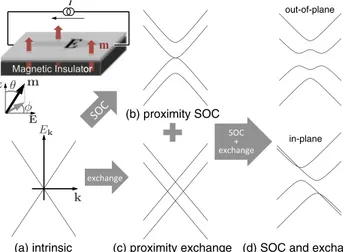
Magnetic Insulator or
m
I
φ θ
E z m
k Ek
FIG. 1. Scheme of magnetoanisotropic transport experiment in proximity graphene. Polar (θ) and azimuthal (φ) angles define the magnetization orientation with respect to the applied electric field.
(a) Linear energy dispersion of pristine graphene can be modified by (b) (intrinsic and Bychkov-Rashba) spin-orbit coupling or (c) exchange field, both leading to spin splitting. (d) The interplay of the two interactions makes the bands anisotropic with respect to the magnetization orientation, here shown as out-of-plane and in-plane.
−40 −20 0 20 40
−40
−20 0 20
(b)40 IP
−40−20 0 20 40
−150
−100
−50 0 50 100 150
energy(meV)
−40−20 0 20 40
−40 −20 0 20 40
−40
−20 0 20
(a)40 OOP
−40−20 0 20 40
−150
−100
−50 0 50 100 150
energy(meV)
−40−20 0 20 40
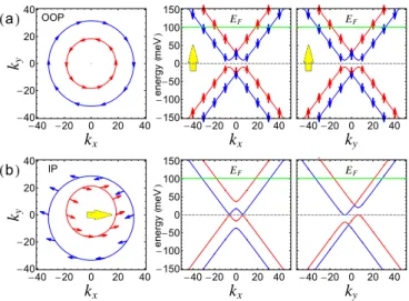
FIG. 2. Fermi contours and spin texture (left), and the band structure along kx (middle) and ky (right) for different directions of the exchange field. The direction of the exchange field is indicated by the large arrows; small arrows give the spin projections. (a) The out-of-plane (OOP) exchange field separates two spin subbands, while the Bychkov-Rashba field leads to a distinctive spin texture depending on the z projection of the real spin, which interacts with exchange field. (b) The in-plane (IP) exchange field splits the bands, but also deforms the Fermi circles. We usedEF =100 meV, λI =0 meV,λBR=10 meV, andλex=25 meV.
minimal Hamiltonian [19]
H=H0+HI+HBR+Hex. (1) Here pristine graphene Hamiltonian is H0=vF(τzσxkx+ σyky) with pseudospin (sublattice) Pauli matrices σσσ and τz= ±1 forK and K points. The Fermi velocity is vF = (3/2)t a0/≈8.6×107 cm/s for t=2.7 eV and the inter- atomic distance of carbons in graphene a0=1.42 ˚A [25].
The proximity intrinsiclike spin-orbit coupling is given by the Hamiltonian HI = −λI +λIτzσzsz, with parameter λI and (true) spin Pauli matrices s. The intrinsic coupling opens a gap of 2λI. The Bychkov-Rashba Hamiltonian HBR= λBR(τzσxsy−σysx), with parameter λBR describes the prox- imity spin splitting due to spin-orbit coupling and lack of space inversion symmetry. Finally, the spin-dependent hybridization with the ferromagnet leads to a proximity exchange Hex= λexm·swith parameterλexand magnetization orientationm.
There are two important magnetic configurations to con- sider: out-of-plane and in-plane magnetizations, depicted in Fig.2(see also Fig.1). In the out-of-plane case the spin up and spin down bands are spin split, but the band structure (and thus Fermi contour) remains isotropic. On the other hand, in the in-plane case the band structure is markedly anisotropic, with the Fermi contours shifted relative to each other.
To investigate electrical transport, we solve the linearized Boltzmann equation for the above model, assuming spatial homogeneity. In the presence of a longitudinal electric field E, the nonequilibrium distribution function isf =f0+δf, where f0 is the equilibrium Fermi-Dirac function. We use the ansatzδf = −e(−∂f0/∂E)u·Eand consider long-range Coulomb scattering, which is the established model for resistivity in graphene [26]. The unknown vectoru is found
by solving the integral equation (obtained from the Boltzmann equation in linear order inE)
v(k)=2π ni(vFrs)2
×
EF
dk
|∇kEk| F(k,k)
q2ε(q)2[u(k)−u(k)], (2) where Ek is the energy corresponding to wave vector k, v(k) is the group velocity, ni is the concentration of scat- terers, the effective fine structure constantrs≈0.8 [27], and F(k,k)= |(k)†(k)|2 is the overlap between the incident (k) and scattered (k) states . For example, for pristine grapheneF(k,k)=(1+cosθkk)/2. For simplicity, spin and pseudospin indices are implicit in the momentum labelsk. The integral is over the Fermi contour of Fermi energyEF, and the transferred momentum isq= |k−k|. The dielectric function εis calculated from the random phase approximation [27–29]
ε(q)
=
1+qqs, if q2kF, 1+π r2s+qqs−qs√
q2−4k2F
2q2 −rssin−12kF
q
, if q >2kF, (3) whereqs=4kFrs. The Fermi wave vectorkF is taken from the pristine graphene case corresponding to a given electron density. The integral equation, Eq. (2), is solved numerically exactly [30], taking the energy spectrum and eigenstates of the effective Hamiltonian, Eq. (1). Knowing vectorsufor the Fermi contour momentak, the conductivity tensor is obtained from
σij = e2 h
dk
2πviujδ(Ek−EF). (4) III. RESULTS AND DISCUSSION
We plot the calculated longitudinal conductivity of graphene as a function of carrier densityn, with and without proximity effects, in Fig.3(a). We useni =80×1010cm−2as a representative density of long-range scatterers. The carrier density, unlike in pristine graphene, depends not only on the Fermi level but also on the strength of the proximity interactionsλI andλex,
n(EF)=2× 1 2π
EF2 +2EFλI+λ2ex (vF)2. (5) The factor 2 takes into account the valley degeneracy. The carrier density is independent of λBR and the direction of the magnetization. In all the plots we fix the carrier density, instead of the Fermi level. The conductivity for three different combinations of parameters is shown in Fig.3(a). The linear dependence onnis well reproduced. WhileλBRandλexbring about relatively insignificant changes (2.5%), the presence of λI =10 meV lowers the conductivity by about∼10% at a fixed carrier density. Thus, in terms of modifying the magnitude of the conductivity, the proximity effects (unless not inducing additional scattering, which would need to be investigated case-by-case) are rather weak, being more pronounced with the inclusion of the intrinsic spin-orbit coupling, than with the Bychkov-Rashba and exchange effects. However, as we will see shortly, the anisotropic effects are quite pronounced.
0 5 10 15 20 25 30 0.0
0.5 1.0 1.5 2.0
(b) 2.5
OOP IP IP
10 inv. spin−galvanic
0 1 2 3 4 5
0 20 40 60 80
(a) 100
FIG. 3. (a) Calculated longitudinal conductivity as a function of carrier density, for pristine and proximity graphene. For proximity graphene we show the conductivity in the presence of Bychkov- Rashba and exchange couplings only, and in the presence of intrinsic spin-orbit coupling only (units in meV). (b) Inverse spin- galvanic effect (scheme in the left inset) in proximity graphene.
Spin density induced (and normalized) by electric field (which is along the x axis) with respect to the exchange interaction, when the magnetization is out-of-plane (OOP) and in-plane (IP).
In-plane magnetization can be either parallel (along the x axis) or perpendicular (along the y axis) to the electric field E. In the right inset, the angle dependance of Sy(φ) is shown in the polar plot withSy =Sy−Sminy , for the electric fieldE=1 V/cm, and for λex=10 meV in percentage with respect to Symax= Sy(E||M). The carrier density in this plot is n=1012 cm−2 and λI =0 meV,λBR=20 meV.
When current flows in the presence of a Bychkov-Rashba field, a spin density transverse to the current appears as a demonstration of the inverse spin-galvanic effect [31–33].
The inverse spin-galvanic effect is the counterpart of the spin-galvanic effect [34–36], which links nonequilibrium spin densitySand electric currentjbyjα=
βQαβSβ, whereQ is a second-rank pseudotensor, andα,β=x,yare coordinate indices. In the inverse spin-galvanic effect, the external electric field that generates steady current shifts the Fermi contour of the separate spin subbands with the helical spin texture due to the Bychkov-Rashba spin-orbit interaction, creating extra population with one spin and reducing the population with the opposite spin. This leads to a homogeneous spin polarization and it is also expected to happen in graphene [37,38]. The nonequilibrium spin density caused by the electric field can be
0
−4
−2 0 2
(b) 4 0
−0.8
−0.6
−0.4
−0.2
(a) 0.0
(% )
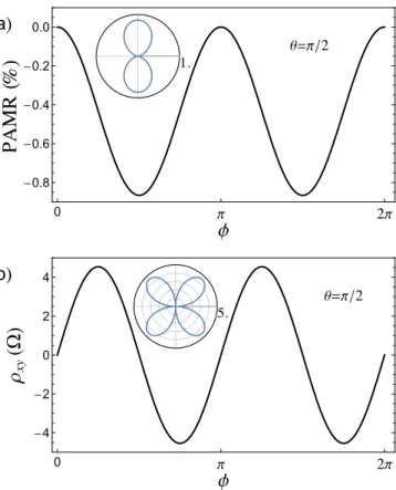
FIG. 4. (a) Calculated proximity induced anisotropic magne- toresistance (PAMR) and (b) planar Hall resistivity are shown when the exchange field is in-plane (θ=π/2) forλBR=20 meV.
PAMR quantifies the longitudinal magnetoresistance as a function of magnetization orientationφ. The interplay of spin-orbit coupling and exchange field leads to a net anisotropic resistivity withC2vsymmetry while the off-diagonal elements of the resistivity tensor are nonzero.
Other parameters aren=1012cm−2, λI=0 meV, λex=10 meV.
The insets are polar plot representations.
calculated as
S= dk
(2π)2δf(k)s(k), (6)
where s(k) is the spin (represented by Pauli matrices s) expectation value of the statek. For our proximity model in the presence of long-range Coulomb scatterers, the calculated inverse spin-galvanic effect is shown in Fig.3(b)as a function of exchange coupling. With increasing magnetization the induced transverse spin is reduced, as the exchange coupling aligns the spins and deforms the rotational spin texture of the Bychkov-Rashba field. The spin densities can be giant.
In fields of 1 V/μm, which are still achievable in graphene, the spin density could reach 1011 cm−2, corresponding to about 10% of spin polarization. The largest induced spin accumulation is in the out-of-plane configuration for large exchange. The magnetoanisotropy of the inverse spin-galvanic effect can be very large, as seen in Fig.3(b). The presence of the current-induced spin accumulation, as well as its magnetoanisotropy, could be detected in the same proximity structure, by measuring the transverse voltage, as in nonlocal spin injection [2].
0 5 10 15 20 25 30 0
5 10 15 20 25
(a) 30
−1 0
0 5 10 15 20 25 30
0 5 10 15 20 25
(b) 30
−4 0
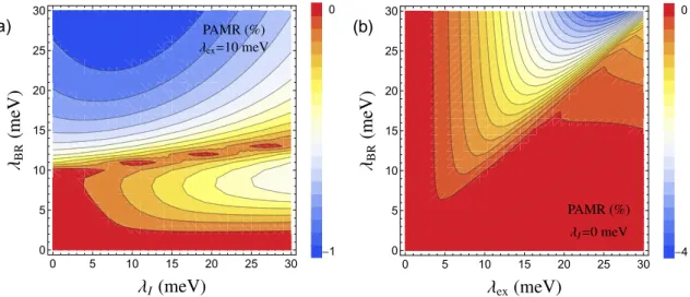
FIG. 5. Parameter maps of PAMR (θ=π/2,φ=π/2). (a) PAMR as a function ofλBRandλI, for a fixedλex=10 meV. (b) PAMR as a function ofλBRandλex, forλI=0 meV. In both maps the carrier density is 1012cm−2.
To quantify the transport magnetoanisotropy, we introduce proximity induced anisotropic magnetoresistance (PAMR)as a ratio of the resistivitiesR (or conductivitiesσ) for a given magnetization orientation (θ,φ) (see Fig.1),
PAMR[E] = R(θ,φ)−R(θ,0)
R(θ,0) = σxx(θ,0)−σxx(θ,φ) σxx(θ,φ) , (7) analogously to the tunneling anisotropic magnetoresistance effect [39–41]. PAMR refers to the changes in the longitudinal magnetoresistance as the magnetization direction varies with respect to the direction of the external electric field that drives the current. When the magnetization is out-of-plane (θ =0), the broken time-reversal symmetry and strong spin-orbit cou- pling can lead to the novel quantum anomalous Hall effect [10], or crystalline magnetoanisotropy [24]. However, here we focus on the regime in which PAMR is most pronounced (θ=π/2).
As shown in Fig.4(a), PAMR exhibits aC2v symmetry due to the interplay between the Bychkov-Rashba and exchange interactions. The expected magnitudes of PAMR are about 1%, similar to what is observed in ferromagnetic metals [24].
The anisotropic resistivity tensor has nonzero off-diagonal elements due to the presence of exchange and spin-orbit couplings. This leads to the planar Hall effect, shown in Fig.4(b). The magnitude of the planar Hall effect could reach up to 4which is greater than the typical values studied in metallic ferromagnetic systems [42].
What values can PAMR reach for a reasonable range of proximity parameters? Figure 5shows two parameter maps, one with the Bychkov-Rashba and intrinsic, the other with the Bychkov-Rashba and exchange couplings. We see two distinct features. (i) First, in Fig.5(a)a horizontal line aroundλBR∼ λex≈10 meV separates two regions. For λBR10 meV, increasing λI increases PAMR. For λBR10 meV, PAMR initially increases with increasingλI, reaching a maximum of
about 1% aroundλI ∼7 meV, beyond which PAMR decreases.
(ii) Second, in Fig. 5(b) the line λBR=λex marks a sharp crossover between weak and strong PAMR. However, this crossover is not uniform. PAMR is largest for large values of bothλexandλBRslightly greater thanλex. The reason why this region gives the largest PAMR (more than 1%) is that in this parameter range there is a band crossing between the strongly spin-orbit coupled subbands.
IV. CONCLUSION
In summary, we used a realistic transport model to pre- dict magnetotransport anisotropies in graphene with proxim- ity exchange and spin-orbit couplings. We predict marked anisotropies in the magnetoresistance, with similar values as reached in ferromagnetic metal junctions and slabs. The calculated PAMR depends strongly on the spin-orbit coupling and exchange parameters. We also calculated the magne- toanisotropies of the planar Hall and inverse spin-galvanic effects. Our systematic investigation over the wide range of parameter set, and the quantitative analysis on magne- toanisotropies in graphene provide practical guidance for experimental demonstration of the aforementioned signatures of magnetotransport. All these magnetoanisotropies should be a sensitive tool to probe proximity effects in graphene that lead to a significant advance toward the graphene spintronics.
ACKNOWLEDGMENTS
We thank Denis Kochan, Jonathan Eroms, and Cosimo Gorini for useful discussions. This work was supported by the DFG SFB 689 and the European Union Seventh Framework Programme under Grant Agreement No. 604391 Graphene Flagship.
[1] M. Gmitra, S. Konschuh, C. Ertler, C. Ambrosch-Draxl, and J.
Fabian,Phys. Rev. B80,235431(2009).
[2] I. ˇZuti´c, J. Fabian, and S. Das Sarma,Rev. Mod. Phys.76,323 (2004).
[3] D. Kochan, M. Gmitra, and J. Fabian,Phys. Rev. Lett. 112, 116602(2014).
[4] J. Bundesmann, D. Kochan, F. Tkatschenko, J. Fabian, and K. Richter,Phys. Rev. B92,081403(2015).
[5] D. Van Tuan and S. Roche,Phys. Rev. Lett.116,106601(2016).
[6] A. Ferreira, T. G. Rappoport, M. A. Cazalilla, and A. H. Castro Neto,Phys. Rev. Lett.112,066601(2014).
[7] J. Wilhelm, M. Walz, and F. Evers,Phys. Rev. B92,014405 (2015).
[8] M. R. Thomsen, M. M. Ervasti, A. Harju, and T. G. Pedersen, Phys. Rev. B92,195408(2015).
[9] H. X. Yang, A. Hallal, D. Terrade, X. Waintal, S. Roche, and M. Chshiev,Phys. Rev. Lett.110,046603(2013).
[10] Z. Qiao, W. Ren, H. Chen, L. Bellaiche, Z. Zhang, A. H.
MacDonald, and Q. Niu,Phys. Rev. Lett.112,116404(2014).
[11] P. Lazi´c, K. D. Belashchenko, and I. ˇZuti´c,Phys. Rev. B93, 241401(2016).
[12] C. B. Crook, C. Constantin, T. Ahmed, J.-X. Zhu, A. V. Balatsky, and J. T. Haraldsen,Sci. Rep.5,12322(2015).
[13] K. Zollner, M. Gmitra, T. Frank, and J. Fabian, arXiv:1607.08008.
[14] K.-H. Jin and S.-H. Jhi,Phys. Rev. B87,075442(2013).
[15] Z. Wang, C. Tang, R. Sachs, Y. Barlas, and J. Shi,Phys. Rev.
Lett.114,016603(2015).
[16] J. C. Leutenantsmeyer, A. A. Kaverzin, M. Wojtaszek, and B. J.
van Wees,arXiv:1601.00995.
[17] J. B. S. Mendes, O. Alves Santos, L. M. Meireles, R. G. Lacerda, L. H. Vilela-Le˜ao, F. L. A. Machado, R. L. Rodriguez-Suarez, A. Azevedo, and S. M. Rezende,Phys. Rev. Lett.115,226601 (2015).
[18] P. Wei, S. Lee, F. Lemaitre, L. Pinel, D. Cutaia, W. Cha, F.
Katmis, Y. Zhu, D. Heiman, J. Hone, J. S. Moodera, and C. T.
Chen,Nat. Mater.15,711(2016).
[19] W. Han, R. K. Kawakami, M. Gmitra, and J. Fabian, Nat.
Nanotechnol.9,794(2014).
[20] M. Trushin and J. Schliemann,Phys. Rev. B75,155323(2007).
[21] O. Chalaev and D. Loss,Phys. Rev. B77,115352(2008).
[22] A. Avsar, J. Y. Tan, T. Taychatanapat, J. Balakrishnan, G. K.
W. Koon, Y. Yeo, J. Lahiri, A. Carvalho, A. S. Rodin, E. C. T.
O’Farrell, G. Eda, A. H. Castro Neto, and B. ¨Ozyilmaz,Nat.
Commun.5,4875(2014).
[23] K. V´yborn´y, A. A. Kovalev, J. Sinova, and T. Jungwirth,Phys.
Rev. B79,045427(2009).
[24] T. Hupfauer, A. Matos-Abiague, M. Gmitra, F. Schiller, J. Loher, D. Bougeard, C. H. Back, J. Fabian, and D. Weiss,Nat. Commun.
6,7374(2015).
[25] N. M. R. Peres,Rev. Mod. Phys.82,2673(2010).
[26] S. Adam, E. H. Hwang, V. M. Galitski, and S. Das Sarma,Proc.
Natl. Acad. Sci. USA104,18392(2007).
[27] E. H. Hwang and S. Das Sarma, Phys. Rev. B 75, 205418 (2007).
[28] E. H. Hwang, S. Adam, S. Das Sarma,Phys. Rev. Lett.98, 186806(2007).
[29] E. H. Hwang and S. Das Sarma,Phys. Rev. B77,195412(2008).
[30] We discretize the Fermi contour (100 to 500 points usually suf- fice) and solve the resulting sets of linear equations algebraically.
[31] S. Ganichev and W. Prettl, Intense Terahertz Excitation of Semiconductors(Oxford University Press, New York, 2006).
[32] S. D. Ganichev and L. E. Golub,Phys. Status Solidi B251,1801 (2014).
[33] J. Borge, C. Gorini, G. Vignale, and R. Raimondi,Phys. Rev. B 89,245443(2014).
[34] S. D. Ganichev, E. L. Ivchenko, V. V. Bel’kov, S. A. Tarasenko, M. Sollinger, D. Weiss, W. Wegscheider, and W. Prettl,Nature (London)417,153(2002).
[35] Ka. Shen, G. Vignale, and R. Raimondi,Phys. Rev. Lett.112, 096601(2014).
[36] J. C. Rojas S´anchez, L. Vila, G. Desfonds, and S. Gambarelli, J. P. Attan´e, J. M. De Teresa, C. Mag´en, and A. Fert, Nat.
Commun.4,2944(2013).
[37] A. Dyrdał, M. Inglot, V. K. Dugaev, and J. Barna´s,Phys. Rev.
B87,245309(2013).
[38] A. Dyrdał, J. Barna´s, and V. K. Dugaev,Phys. Rev. B89,075422 (2014).
[39] A. Matos-Abiague, M. Gmitra, and J. Fabian,Phys. Rev. B80, 045312(2009).
[40] A. Matos-Abiague and J. Fabian, Phys. Rev. B 79, 155303 (2009).
[41] L. Brey, C. Tejedor, and J. Fern´andez-Rossier,Appl. Phys. Lett.
85,1996(2004).
[42] H. X. Tang, R. K. Kawakami, D. D. Awschalom, and M. L.
Roukes,Phys. Rev. Lett.90,107201(2003).