Theory of electronic and spin-orbit proximity effects in graphene on Cu(111)
Tobias Frank,*Martin Gmitra, and Jaroslav Fabian
Institute for Theoretical Physics, University of Regensburg, 93040 Regensburg, Germany (Received 11 January 2016; revised manuscript received 31 March 2016; published 22 April 2016) We study orbital and spin-orbit proximity effects in graphene adsorbed to the Cu(111) surface by means of density functional theory (DFT). The proximity effects are caused mainly by the hybridization of grapheneπ and copperdorbitals. Our electronic structure calculations agree well with the experimentally observed features.
We carry out a graphene-Cu(111) distance dependent study to obtain proximity orbital and spin-orbit coupling parameters, by fitting the DFT results to a robust low energy model Hamiltonian. We find a strong distance dependence of the Rashba and intrinsic proximity induced spin-orbit coupling parameters, which are in the meV and hundreds ofμeV range, respectively, for experimentally relevant distances. The Dirac spectrum of graphene also exhibits a proximity orbital gap, of about 20 meV. Furthermore, we find a band inversion within the graphene states accompanied by a reordering of spin and pseudospin states, when graphene is pressed towards copper.
DOI:10.1103/PhysRevB.93.155142
I. INTRODUCTION
Copper is an important material for graphene. Graphene- copper junctions are often encountered in technological applications [1,2]. For example, graphene can be used to seal a copper surface to preserve its excellent plasmonic characteristics [3]. The growth of graphene via CVD by the deposition of CH4 on copper surfaces is amongst the most popular techniques to obtain large (poly)crystalline graphene [4]. Even single layer graphene grains of millimeter size as well as pyramidlike bi- and trilayer graphene, hexagonal onion-ring-like graphene grains can be grown on copper [5,6].
Important to our study, graphene produced on a copper surface exhibits a giant spin Hall effect, likely due to residual copper adatoms and adclusters [7].
Experimentally, graphene on the Cu(111) surface has been well studied by means of angle-resolved photoemission spec- troscopy (ARPES) [8–14] and scanning tunneling microscopy (STM) [4]. The linear dispersion of graphene is found to be preserved. ARPES measurements of the graphene-Cu(111) system find that graphene is getting electron doped [14], leading to a shift of the Dirac energy ED, which we define as the average energy of the grapheneπ state energies at K with respect to the Fermi energyEF. Typically,EDis about
−0.3 eV with respect to the Fermi energy [14]. The top of thed band edge of copper begins at−2 eV below the Fermi level. It is observed that a gap opens within the Dirac cone of graphene of about 50–180 meV [8,10–14].
Spin-orbit coupling (SOC) effects in graphene on selected metal substrates were studied theoretically [15,16] and experi- mentally [17,18], and it was noticed that substrates can induce sizable spin-orbit effects important for spintronics applica- tions [19,20]. Spin resolved ARPES experiments [11] focused on the spin-orbit effects introduced by metallic surfaces in graphene, investigating the role of the atomic number of the substrate. It was found that the states of graphene can be split due to Rashba spin-orbit coupling by up to 100 meV in the case of Au and 10 meV in the case of Ni [16], respectively.
Copper substrate induced spin-orbit splittings in graphene are
*tobias1.frank@physik.uni-regensburg.de
expected to be substantially smaller [11]. They were measured at a temperature of 40 K, which gives a resolution limit and also the upper bound for the spin-orbit effects of 3.4 meV. The mechanism introducing the spin-orbit interaction was identi- fied to be the hybridization between substratedand grapheneπ states [11]. Our present paper agrees with this conclusion and predicts the values of the Rashba splitting to be about 2 meV for a reasonable distance between graphene and copper, just below the stated experimental resolution of Ref. [11].
Crucial to obtain accurate graphene-metal distances is to consider van der Waals interactions. It was found [21–23] that the dispersive long-range interactions play an important role in binding, yielding graphene-copper distances of 2.91 to 3.58 ˚A.
Here, we focus on hybridization and proximity effects by means of DFT calculations. By the application of an effective Hubbard U [24], which corrects for self interaction errors, we achieve a good agreement with experiment in terms of the emission spectra and the band structure features. We carry out an analysis of the orbital composition of the band structure, giving us hints for a model Hamiltonian including spin-orbit interactions, which can be used to describe graphene in combination with many other materials that yield aC3v or higher symmetric system. We then fit the model Hamiltonian to the DFT data and extract parameters such as the induced gap as well as spin-orbit coupling values. As the graphene-copper distance is not exactly known experimentally, and there is still a theoretical uncertainty in determining its magnitude, we carry out a distance-dependent study.
Our main finding is a strong graphene-Cu(111) distance- dependent spin-orbit coupling introduced in the graphene states. We use a model Hamiltonian to describe those states, for which we observe a Rashba spin-orbit coupling parameter which reaches values of meVs, while being absent in pristine graphene. The proximity induced intrinsic SOC is in the hundreds ofμeV range, a factor of ten larger than in pristine graphene. We also observe a closing of the induced gap for a graphene-copper distance of 2.4 ˚A. This is accompanied by a peculiar reordering of spin and pseudospin states associated with a gap inversion at small distances.
The paper is organized as follows. SectionIIdeals with the computational methods used. Geometrical structure modeling is described in Sec.III A. In Sec.III Bwe carry out the analysis
of the band structure. In Sec. III C we introduce our model Hamiltonian and fit it to theab initiodata. Finally, in Sec.III D we present our graphene-copper distance dependent study with a discussion of the proximity induced effects.
II. COMPUTATION METHODS
We used DFT implemented in the plane-wave codeQUAN-
TUM ESPRESSO [25]. The calculations were performed at a k point sampling of 40×40 if not indicated otherwise. A slab geometry was applied, where we added a minimum of 15 ˚A of vacuum around the structure in the z direction.
We used the Kresse-Joubert ultrasoft (relativistic) PBE [26]
projector augmented wave pseudopotentials [27]. The plane wave energy cutoff was set to 40 Ry and the charge density cutoff to 320 Ry to ensure converged results. Van der Waals interactions were taken into account using the empirical method of Grimme [28]. To cross-check spin-orbit coupling calculations we also employed the all electron, full potential linearized augmented plane wave codeWIEN2K. [29] We found that spin-orbit coupling splittings were differing at most by 10%. For processing our distance studies the atomic simulation environment (ASE) [30] was used. Hellmann-Feynman forces in relaxed structures were decreased until they were smaller than 0.001 Ry/a0. Calculations for graphene on Cu(111) included calculations adding the HubbardUcorrection [31].
III. GRAPHENE Cu(111) STUDY A. Choice of unit cell
The mismatch between Cu(111)’s surface lattice constant of 3.61/√
2 ˚A [32] and graphene’s lattice constant of 2.46 ˚A is 3.8%. STM experiments [4] observe regions with different moir´e structures; the most observed one (30%) is a commen- surate lattice configuration with a periodicity of 66 ˚A. Another experiment [8] found that 60% of graphene grains on Cu(111) are preferentially rotated by 3◦ with respect to the substrate.
To account for the lattice mismatch, one would have to chose a unit cell, which is computationally very demanding, containing hundreds of atoms. We set the lattice constant of copper to be compatible with the experimental graphene lattice constant, to describe graphene as realistically as possible, following Ref. [2]. A supporting fact to use graphene’s lattice constant is that graphene does not chemically bind to copper and its strong in-planeσ bonds remain intact.
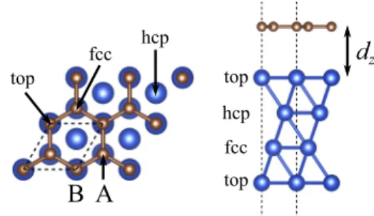
In the transverse direction to the Cu(111) surface one dis- tinguishes three nonequivalent Cu planes. We label the planes from the surface towards bulk as top, hcp, and fcc, see Fig.1.
We tested three different commensurate configurations named according to which Cu layer the carbon atoms sit over. This gives rise to three possible graphene physisorbed positions named as top-fcc, top-hcp, and fcc-hcp configurations [2]. In Fig.1we show the top-fcc configuration, where one carbon atom (say from sublattice B) is on top of a copper atom of the top layer, while the other carbon (from sublattice A) is over the fcc Cu layer.
In general, the graphene sublattices have different environ- ments. This breaks the sublattice symmetry of graphene and re- sults in sublattice resolved spin-orbit coupling effects [33,34].
To simulate a copper surface we used four layers of copper.
B A
top
fcc hcp
d
z tophcp fcc top
FIG. 1. Structure: Top and side views of the unit cell, which is indicated as black dashed lines, repeated twice in each lateral direction. Blue (large) spheres indicate the copper atoms, brown (small) spheres the carbon atoms. The sublattice is depicted by labels A and B. The copper layers are labeled by top, hcp, and fcc, which also tag the adsorption positions.
We checked that the physics of the graphene low energy states does not change upon increasing the number of layers. In addition, we found good agreement of the band structure with experiment [8–14].
In our studies we first relaxed the copper slabalonewithout van der Waals corrections and then fixed its degrees of freedom and let just the carbon atoms relax in thezdirection including empirical van der Waals corrections. [28] To start with, the copper slab is strained in thexy plane such that its surface lattice constant aCu/√
2 is the same as the experimental graphene lattice constant of 2.46 ˚A yielding an effective bulk lattice constant ofaCu=3.48 ˚A. This represents a compression of the copper slab by 3.8% with respect to the bulk value of 3.61 ˚A [32]. After letting the copper slab relax in the z direction, the distance of copper atoms from plane to plane was 2.59 ˚A, corresponding to an expansion of 1.7% compared to bulk copper. This compensates to some extent for the compression in thexyplane.
Comparing the top-fcc with the other commensurate con- figurations top-hcp and fcc-hcp we found slightly different graphene-Cu(111) distancesdzof 3.10 ˚A, 3.11 ˚A, and 3.12 ˚A, respectively. The corrugation of the carbon atoms inzdirection is less than 10−3 A, expressing the weak nature of binding.˚ The lowest energetic configuration is the top-fcc arrangement, followed by the top-hcp, which is only 2.3 meV higher in energy per unit cell. The highest one in total energy with 12.3 meV compared to top-fcc is fcc-hcp, where the nearest copper atom sits within the carbon ring. Therefore in the following study we consider the top-fcc configuration.
B. Choice of methods and electronic structure
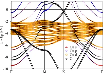
The orbital resolved electronic structure of graphene on Cu(111) is shown in Fig.2for DFT+Uwith an effectiveU = 1 eV [31] acting on the Cu 3delectrons for a copper-graphene distance of 3.09 ˚A. It can be seen, that the Dirac cone structure is preserved for energies higher than−2 eV. Below this energy region the grapheneπstates hybridize with the copperdstates.
This can be seen by the avoided crossings if one follows theπ band towards thepoint at−8.5 eV. On this way, at−6 eV theπstates branch and strongly hybridize with a copper band consisting ofpandsstates. Those are states which are situated on the surfaces of the slab and whose degeneracy is broken due
-10 -8 -6 -4 -2 0
Γ M K Γ
E - EF [eV]
Cu s Cu p Cu d C
FIG. 2. Calculated electronic structure of graphene/Cu(111) slab. The graphene distance from Cu(111) surface is 3.09 ˚A. The overlaying symbols indicate orbital resolved contributions to the eigenvalues. Orange pentagons show Cudbands, red upward pointing triangles represent Cusstates, blue squares show Cup states and black downward pointing triangles indicate graphene states.
to the graphene potential. The grapheneσ states starting from
−3.5 eV at thepoint are mainly unaffected. The coppers andpstates are present in the energy region between−9.5 eV and−6 eV as well as from−2 eV and upwards. The copper band structure obtained here is qualitatively in agreement with bulk fcc calculations. The position of the Fermi energy was converged for a dense sampling of the Brillouin zone.
There is charge transfer from the Cu(111) surface to graphene. As a result, graphene getsndoped [2]. We compared the effect of the relaxation of copper slabs in thezdirection for the relaxed and nonrelaxed (bulk lattice constant of 3.48 ˚A) cases on the doping of graphene. For nonrelaxed (compressed) copper slabs the electron doping of graphene was significantly higher than for relaxed slabs due to the higher kinetic energy in nonrelaxed copper. For relaxed copper slabs the Dirac energy shift is comparable to experiment [4], being−350 meV.
To account for correlation effects, we applied a Hubbard U correction of 1 eV to the copperd states. In this way we match the onset of the completely filled copperdlevels, which show up at −2 eV below the Fermi energy in the ARPES experiments [8,10,11]. The effect of the HubbardUcorrection is a rigid shift of the filled copperd levels to lower energies without changing their band widths. However, we see a strong dependence of the copperdlevel energies on the compression of the copper slab, they are 1 eV higher in energy for the compressed than for the relaxed one. The proper position of thed levels is significant for the spin-orbit coupling induced proximity effect in the Dirac cone, as there can be larger hy- bridization, when thedlevels are closer to the states of interest.
All in all we find a good agreement of the band structure with experiment [8]. The only shortcoming is the description of the graphene gap, which is opening at the Dirac energyED. We find it to be 20 meV, which is lower than the 50 to 180 meV stated in experiments [8,10–14]. This deviation could be due to the limitations of semilocal and local exchange-correlation functionals.
C. Model Hamiltonian
As we demonstrated above, DFT+U reasonably captures the electronic structure of graphene on the Cu(111) surface.
Now we use the first-principles calculations to predict prox- imity induced effects of the copper surface on the spin-orbit coupling in graphene. For this purpose we study a Hamiltonian describing the low energyπ states of graphene on Cu(111).
The HamiltonianH=Horb+Hso contains orbital and spin- orbit coupling parts and describes graphene whose symmetry point group is lowered fromD6h(pure graphene) toC3v. Such a Hamiltonian was introduced already in the context of hy- drogenated graphene [33] in which the pseudospin symmetry gets broken explicitly by hydrogenation, but it was also found useful in graphene whose pseudospin is broken implicitly only, by placing graphene on incommensurate lattices such as MoS2[34]. In our case the pseudospin symmetry is broken explicitly as the pseudospin state is well defined but the two sublattices experience a different orbital environment, see Fig.1. This proximity Hamiltonian has the form,
Horb=vF(κσxkx+σyky)+σzs0, (1) and
Hso =λAI[(σz+σ0)/2]κsz+λBI[(σz−σ0)/2]κsz (2) +λR(κσxsy−σysx), (3) wherevFis the Fermi velocity andκ =1(−1) labels the valley degree of freedom.kxandkyare the Cartesian components of the electron wave vector measured from K(K),σx andσy are the pseudospin Pauli matrices acting on the two-dimensional vector space formed by the two triangular sublattices of graphene. The first term inHorbdescribes gapless Dirac states.
The second term describes the effective orbital hybridization energy, which acts as a staggered potential on sublattices A and B, whereσzis the pseudospin Pauli matrix ands0 is the unit matrix in spin space. This Hamiltonian term leads to an orbital proximity induced gap in the Dirac spectrum of 2. This gap is still present even when spin-orbit coupling is turned off.
A consequence of the pseudospin inversion asymmetry is the sublattice-resolved intrinsic spin-orbit coupling. As intrinsic spin-orbit coupling is a next-nearest neighbor hopping, it acts solely on a given sublattice. We describe it with parameters λAI andλBI for sublattice A and B, respectively. We denote by sz the spin Pauli matrix and byσ0 the unit matrix acting on the pseudospin space. IfλAI =λBI, the spin degeneracy gets lifted already by this intrinsic term, reflecting the loss of space inversion symmetry. The space inversion asymmetry itself gives rise to Rashba type spin-orbit coupling whose strength is measured byλR, which is a nearest-neighbor spin-flip hopping, contributing further to the spin splitting of the low energy bands.
The four eigenvalues of the model Hamiltonian at the K point (k=0) read
ε4= −1 2λ+I +
−1
2λ−I 2
+4λ2R,
ε3=+1
2(λ+I +λ−I ),
−0.06
−0.04
−0.02 0 0.02 0.04 0.06
0.4 0.2 0 0.2 0.4
E − ED [eV]
k [10−2/Å]
Γ← →M
model fit DFT
FIG. 3. Calculated band structure around Dirac point. Com- parison of DFT calculations with the model calculations for a graphene-copper distance of 3.09 ˚A. The energy is measured with respect to the Dirac energyED. The plot is centered at K (k=0) and its left part corresponds to thekpoints pointing towardsand the right part towards the M point.
ε2 = −+1
2(λ+I −λ−I ), ε1 = −1
2λ+I −
−1 2λ−I
2 +4λ2R,
whereλ+I =λAI +λBI andλ−I =λAI −λBI for compactness. We ordered the eigenvalues by decreasing energies, where we assumedλRλAI, λBI. The eigenstatesε2andε3always have spin-zexpectation values ofsz= −1/2 andsz=1/2, and pseudospin-zexpectation values ofσz= −1/2 andσz=1/2 and are localized on sublattice B and A, respectively. The eigenstates withε1andε4in general are mixtures of sublattices and spin directions, but have almostsz1/2,σz −1/2 and sz −1/2, σz1/2 under the assumption thatλR λAI , λBI. In the model Hamiltonian there are four unknown parameters. To construct a set of independent equations we also take into account the spin-zexpectation value for the first eigenstate denoted bys1z. The model parameters thus can be expressed as follows:
=14
−ε2+ε3−2s1z(ε1−ε4) , λAI =14
−ε1+2ε3−ε4+2s1z(ε1−ε4) , λBI =14
−ε1+2ε2−ε4−2s1z(ε1−ε4) , λR=14(ε1−ε4)
1−4
s1z2
.
We note that special care has to be taken when associating the order of the DFT eigenvalues with respect to the model Hamiltonian eigenvalues. For every state we compared the sublattice localization and sz values for both the DFT and model calculations.
In Fig.3we compare low energy graphene bands calculated from DFT and model, for a distance of dz=3.09 ˚A. The fitted model parameters are=9.3 meV,λAI = −0.131 meV, λBI =0.060 meV, andλR=1.2 meV. The proximity effects, both the orbital and spin-orbit coupling ones, are significant.
The hybridization gapdominates the energy scale. It yields a
0.5 1 1.5 2 2.5
0.4 0.2 0 0.2 0.4
ΔE [meV]
k [10−2/Å]
Γ← →M
model cond. band model val. band DFT
cond. band DFT val. band
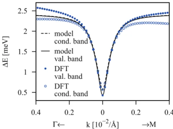
FIG. 4. Calculated spin splittings of the valence and conduction bands. The DFT data is shown by symbols while the lines correspond to the model description. The distance between graphene and copper is 3.09 ˚A.
gap value ofEgap=ε3−ε2≈2=18.6 meV. The Rashba spin-orbit coupling parameter of 1.2 meV indicates a very strong effect of the space inversion asymmetry, which would correspond to a transverse electric field of 240 V/nm for bare graphene [35]. The intrinsic spin-orbit coupling parameters have opposite sign and their amplitudes are significantly en- hanced in comparison to the tens ofμeV in bare graphene [35].
The Fermi velocity isvF=0.825×10⁶m/s (equivalent to a nearest neighbor hopping of 2.55 eV). We see that the band structure is isotropic in this range ofkpoints and the model description agrees very well with the DFT data. We observed a good agreement up to energies±0.1 eV away from the Dirac energy.
We also compare the band spin splittings of the valence and conduction bands, see Fig.4. It can be seen that by construction the splittings at K are described exactly. The model reproduces very well the narrowing of the band splittings forkpoints up to 0.1×10⁻²/A away from the K point even though only˚ information from the K point enters. As the model does not include spin-orbit coupling terms dependent on k, both the valence and conduction band splittings from the model calculations saturate at a common value for largerk due to the Rashba SOC. To include k dependent terms one needs to consider terms such as pseudospin inversion asymmetry (PIA) [33,34,36] which can capture the k dependence of the splittings. In the DFT calculations we observed that the splittings for valence (conduction) bands increase (decrease) with larger distances from K as the interaction with copperd levels increases (decreases) and the induced spin-orbit effects are stronger (weaker).
D. Distance study
Standard DFT cannot account for dispersive forces. Differ- ent methods dealing with van der Waals effects often yield inconsistent results [21–23] when trying to treat graphene on metal surfaces. Therefore, we conduct calculations of electronic properties for different graphene-Cu(111) distances.
We used the Hubbard correction [31] with U=1 eV for Cud electrons. The relative coordinates of the atoms within the copper slab and within graphene were fixed and the
0.1 0 0.2 0.3 0.4 0.5 0.6 0.7 0.8
2 2.2 2.4 2.6 2.8 3 3.2 3.4 3.6 3.8 (a) Etot − E0 [eV]
−1
−0.8
−0.6
−0.4
−0.2 0 0.2 0.4
2 2.2 2.4 2.6 2.8 3 3.2 3.4 3.6 3.8 (b) ED [eV]
−30
−20
−10 0 10 20 30
2 2.2 2.4 2.6 2.8 3 3.2 3.4 3.6 3.8 (c)
Gap, Rashba [meV]
ΔλR
−∂λR/∂dz
0.001 0.01 0.1 1 10
2 2.2 2.4 2.6 2.8 3 3.2 3.4 3.6 3.8 (d)
Intrinsic [meV]
−λI A
λI B
−0.5 0 0.5
2 2.2 2.4 2.6 2.8 3 3.2 3.4 3.6 3.8 (e) sz
distance [Å]
1 4
−0.5 0 0.5
2 2.2 2.4 2.6 2.8 3 3.2 3.4 3.6 3.8 (f) sz
distance [Å]
2 3
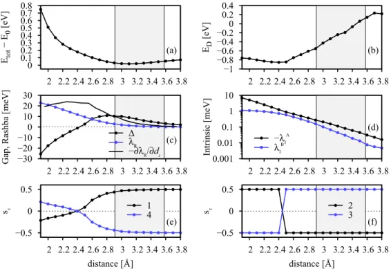
FIG. 5. Calculations of low energy properties of graphene on Cu(111) surface as a function of distance, with a HubbardUof 1 eV used.
(a) Total energy with respect to the minimal total energy at 3.09 ˚A; (b) Dirac energy shiftEDwith respect to Fermi level; (c) proximity induced potentialand Rashba spin-orbit coupling parameterλR, as well as the derivative ofλR; (d) intrinsic spin-orbit coupling parametersλAI and λBI; (e) spinszexpectation values for theε1andε4graphene eigenvalues at the K point and (f) for theε2andε3eigenvalues. The shaded region indicates predicted distances from other theoretical references [21–23].
graphene-copper distancedzwas varied. We apply the same analysis as in Sec. III C for each distance configuration dz
and extract the total energy of the structure, the Dirac energy shiftED, the hybridization gap , the Rashba and intrinsic spin-orbit coupling parameters as well as spin-zexpectation values of the graphene states at the K point.
In Fig.5(a)we show the total energy as a function of the graphene distance dz from the Cu(111) surface. The curve is shifted with respect to the minimal total energy at the distance of 3.09 ˚A. The energy dependence has a rather shallow minimum where the energy increases by just 0.5 eV when graphene is pushed to a distance of 2 ˚A.
Figure 5(b) visualizes the shift of the Dirac energy ED with respect to the Fermi level. We see that graphene stays ndoped for distances smaller than 3.5 ˚A, and the curve has two regimes. For larger distances down to 2.5 ˚A there is a linear behavior with a positive slope, the more graphene is pushed towards the Cu(111) surface, the morendoped it gets.
For distances smaller as 2.5 ˚A the slope reverses its sign and is more shallow. This means that there occurs a significant charge transfer from the copper slab to the graphene sheet, which saturates at smaller distances.
Figure5(c)shows the values for the proximity induced po- tentialand the Rashba spin-orbit parameterλR. The Rashba parameter is increasing steadily with decreasing distance. We also plot the derivative of the Rashba parameter with respect to the distance−∂λR/∂dz. One sees that the Fermi level shift and the change in the Rashba parameter are correlated by comparing the derivative of the Rashba parameter to the Fermi level shift. Both curves change their trend at 2.5 ˚A. We can
see that the origin of the Rashba spin-orbit coupling is due to charge doping (determined by the Fermi energy shiftED), leading to a built-in electric field, and due to the positioning of the graphene sheet in the electrostatic potential of the Cu(111) surface. At the distance of 2.5 ˚A the charge doping stops, and therefore the Rashba spin-orbit coupling increases at a lower pace. It remains increasing though, as the graphene sheet resides in a potential which becomes steeper as it gets closer to the nuclei of copper. It is surprising that the, which first increases from larger to smaller distances, decreases, becomes zero at 2.4 ˚A and then inverts its sign. We will discuss this in more detail later. We estimate the pressurepone would have to exert on graphene to reach this distance as
p= E
dz·A = 200 meV
(3.09−2.40) ˚A·(2.46 ˚A)2·sin 60◦
=8.8 GPa,
where E is the energy difference between the lowest energetic state and the state where the transition happens,dz
their distance difference, andAis the area of the unit cell. The bulk modulus of copper for comparison is 184 GPa [37].
The amplitudes of the intrinsic spin-orbit coupling pa- rametersλAI andλBI strongly increase as graphene is pushed towards the Cu(111) surface, see Fig.5(d). For large distances both parameters tend to values comparable in size as in pure graphene. For smaller distances the sublattice asymmetry transfers to the parameters andλAI is much stronger affected due to the specific graphene sublattice positioning on Cu(111).
λAI reaches values up to 7 meV, whereasλBI stays smaller than
~B B A
~A
~A A B
~B small distance large distance
increasing pressure
K 2.4 K
FIG. 6. Scheme visualizing the transition of spin states at K with vertical pressure. Black solid lines indicate the energy levels, A and B stands for the sublattice. Arrows pointing upwards (downwards) represent spins pointing alongz(−z), shorter arrows indicate spin mixture and their projection to thezdirection.
1 meV for all tested distances and tends to saturate at 1 meV when reaching a small distance of 1.8 ˚A.
The last two panels in Figs. 5(e) and 5(f) show the spin-zexpectation values at K for the eigenvaluesεi, where 1 labels the lowest energy and 4 the highest energy state.
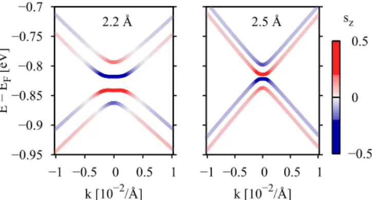
From Fig. 5(e) we can see that the outermost expectation values represent spin states of mixed spin, as values of spin 1/2 are only reached, when graphene is well separated from copper. The spin expectation values of states 2 and 3 are pure states and are always quantized in thezdirection. When the hybridization gap closes, at 2.4 ˚A, we observe that the signs of all spin expectation values change abruptly. This behavior is exemplified in Fig.6. When the distance of graphene to copper is decreased, the spin as well as pseudospin signs change.
In Fig.7we show the topology of the bands obtained from DFT calculations around K for distances of 2.2 and 2.5 ˚A, with the corresponding spin-zexpectation values. The plot is consistent with Figs.5(e)and5(f), for 2.5 ˚A the band structure resembles the one in Fig. 3 and has spin up-down-up-down sequence, where the inner eigenstates have pure sz= ±1/2 components. The spin-zcharacter within the bands stays the same. The band structure topology for 2.2 ˚A is different. At the K point the inner eigenstates again have puresz= ∓1/2 spin, but all signs are reversed. Furthermore, the spin-zcharacter is not preserved within the bands. There is evidence for a band inversion for the inner bands with a significant spin mixing to outermost bands. The spin reversal is accompanied by a change of the pseudospin character of the states. The valence states become localized on the A sublattice and conduction bands on sublattice B. We note that similarly to the spin mixing for the outermost bands, the states are also sublattice mixed, which is also depicted in Fig. 6. Our model is able to reproduce the spin-zbehavior of Fig.7 (not shown here).
The band inversion could have impact on the topology of the system, a spin Hall to quantum spin Hall phase transition might happen. However in this system there are metallic states present, which prevent a classification in terms of trivial and topological insulating phases. We note that the transition could be easier achieved, when graphene is put on gold, as there the spin-orbit effects are much stronger and the electronic structure is similar [11]. We also would like to stress that in experiments, regions with different configurations as top-hcp and fcc-hcp are likely due to the appearance of moir´e patterns.
−0.95
−0.9
−0.85
−0.8
−0.75
−0.7
−1 −0.5 0 0.5 1 2.2 Å
E − EF [eV]
k [10−2/Å]
−1 −0.5 0 0.5 1 sz 2.5 Å
k [10−2/Å]
−0.5 0 0.5
FIG. 7. Band structure topologies of graphene on Cu(111) for 2.2 ˚A and 2.5 ˚A distances of graphene from the Cu(111) surface.
The spinszexpectation values for the states are encoded by the color scale, where red color denotes spin-zexpectation value of 1/2 and blue color denotes a spin-zexpectation value of−1/2.
We cross-checked the distance dependence for top-hcp and fcc-hcp and found that spin-orbit coupling parameters have the same order of magnitude. The similar configuration top-hcp exhibits the same kind of spin and pseudospin transition as top-fcc. For the energetically higher configuration fcc-hcp, the transition is absent at distances from 1.9 to 3.8 ˚A.
IV. SUMMARY
We have shown that the electronic band structure measured by ARPES is reasonably described by DFT+U calculations.
We are able to correctly describe the Fermi level position and copperd band onset. Based on this good orbital description we predict the spin-orbit coupling effects by analyzing the low energy graphene states using a robust model Hamiltonian.
We show that our Hamiltonian is able to describe the spin-orbit induced band splittings even away from the K point. We extracted spin-orbit coupling parameters as well as spin expectation values dependent on the graphene-copper distance and found a strong distance-dependent behavior of spin-orbit coupling parameters and a reordering of the spin and pseudospin structure at the Dirac point atdz=2.4 ˚A. At low distances the Dirac band structure gets inverted due to the overlap of opposite spin valence and conduction bands. Our findings are experimentally verifiable with techniques such as ARPES, by increasing the resolution to resolve the meV and sub meV spectral ranges.
ACKNOWLEDGMENTS
This work was supported by the DFG SFB Grant No.
689 and GRK Grant No. 1570, and by the EU Seventh Framework Programme under Grant Agreement No. 604391 Graphene Flagship. The authors gratefully acknowledge the Gauss Centre for Supercomputing e.V. (www.gauss-centre.eu) for funding this project by providing computing time on the GCS Supercomputer SuperMUC at Leibniz Supercomputing Centre (LRZ,www.lrz.de).
[1] G. Giovannetti, P. A. Khomyakov, G. Brocks, V. M. Karpan, J. van den Brink, and P. J. Kelly,Phys. Rev. Lett.101,026803 (2008).
[2] P. A. Khomyakov, G. Giovannetti, P. C. Rusu, G. Brocks, J.
van den Brink, and P. J. Kelly, Phys. Rev. B 79, 195425 (2009).
[3] V. G. Kravets, R. Jalil, Y.-J. Kim, D. Ansell, D. E. Aznakayeva, B. Thackray, L. Britnell, B. D. Belle, F. Withers, I. P. Radko, Z. Han, S. I. Bozhevolnyi, K. S. Novoselov, A. K. Geim, and A. N. Grigorenko,Sci. Rep.4,5517(2014).
[4] L. Gao, J. R. Guest, and N. P. Guisinger,Nano Lett.10,3512 (2010).
[5] Z. Yan, Z. Peng, and J. Tour, Acc. Chem. Res. 47, 1327 (2014).
[6] D. Boyd, W.-H. Lin, C.-C. Hsu, M. Teague, C.-C. Chen, Y.-Y.
Lo, W.-Y. Chan, W.-B. Su, T.-C. Cheng, C.-S. Chang, C.-I. Wu, and N.-C. Yeh,Nat. Commun.6,6620(2015).
[7] J. Balakrishnan, G. K. W. Koon, A. Avsar, Y. Ho, J. H. Lee, M. Jaiswal, S.-J. Baeck, J.-H. Ahn, A. Ferreira, M. A. Cazalilla, A. H. C. Neto, and B. ¨Ozyilmaz,Nat. Commun.5,4748(2014).
[8] J. Avila, I. Razado, S. Lorcy, R. Fleurier, E. Pichonat, D.
Vignaud, X. Wallart, and M. C. Asensio,Sci. Rep. 3, 2439 (2013).
[9] C. Jeon, H.-N. Hwang, W.-G. Lee, Y. G. Jung, K. S. Kim, C.-Y.
Park, and C.-C. Hwang,Nanoscale5,8210(2013).
[10] A. J. Marsden, M.-C. Asensio, J. Avila, P. Dudin, A. Barinov, P. Moras, P. M. Sheverdyaeva, T. W. White, I. Maskery, G.
Costantini, N. R. Wilson, and G. R. Bell,Phys. Status Solidi RRL7,643(2013).
[11] A. M. Shikin, A. G. Rybkin, D. Marchenko, A. a. Rybkina, M. R. Scholz, O. Rader, and A. Varykhalov,New J. Phys.15, 013016(2013).
[12] A. Varykhalov, M. R. Scholz, T. K. Kim, and O. Rader,Phys.
Rev. B82,121101(R) (2010).
[13] H. Vita, S. B¨ottcher, K. Horn, E. N. Voloshina, R. E.
Ovcharenko, T. Kampen, A. Thissen, and Y. S. Dedkov, Sci. Rep.4,5704(2014).
[14] A. L. Walter, S. Nie, A. Bostwick, K. S. Kim, L. Moreschini, Y. J.
Chang, D. Innocenti, K. Horn, K. F. McCarty, and E. Rotenberg, Phys Rev. B84,195443(2011).
[15] S. Abdelouahed, A. Ernst, J. Henk, I. V. Maznichenko, and I.
Mertig,Phys. Rev. B82,125424(2010).
[16] Z. Y. Li, Z. Q. Yang, S. Qiao, J. Hu, and R. Q. Wu,J. Phys.
Condens. Matter23,225502(2011).
[17] O. Rader, A. Varykhalov, J. S´anchez-Barriga, D. Marchenko, A.
Rybkin, and A. M. Shikin,Phys Rev. Lett.102,057602(2009).
[18] D. Marchenko, A. Varykhalov, M. R. Scholz, G. Bihlmayer, E. I.
Rashba, A. Rybkin, A. M. Shikin, and O. Rader,Nat. Commun.
3,1232(2012).
[19] I. ˇZuti´c, J. Fabian, and S. D. Sarma,Rev. Mod. Phys.76,323 (2004).
[20] W. Han, R. K. Kawakami, M. Gmitra, and J. Fabian,Nat. Nano 9,794(2014).
[21] T. Olsen and K. S. Thygesen,Phys. Rev. B87,075111(2013).
[22] M. Vanin, J. J. Mortensen, A. K. Kelkkanen, J. M. Garcia-Lastra, K. S. Thygesen, and K. W. Jacobsen,Phys. Rev. B81,081408(R) (2010).
[23] M. Andersen, L. Hornekaer, and B. Hammer,Phys. Rev. B86, 085405(2012).
[24] V. I. Anisimov, J. Zaanen, and O. K. Andersen,Phys. Rev. B44 943(1991).
[25] P. Giannozzi, S. Baroni, N. Bonini, M. Calandra, R. Car, C.
Cavazzoni, D. Ceresoli, G. L. Chiarotti, M. Cococcioni, I.
Dabo, A. Dal Corso, S. de Gironcoli, S. Fabris, G. Fratesi, R.
Gebauer, U. Gerstmann, C. Gougoussis, A. Kokalj, M. Lazzeri, L. Martin-Samos, N. Marzari, F. Mauri, R. Mazzarello, S.
Paolini, A. Pasquarello, L. Paulatto, C. Sbraccia, S. Scandolo, G. Sclauzero, A. P. Seitsonen, A. Smogunov, P. Umari, and R. M. Wentzcovitch, J. Phys. Condens. Matter 21, 395502 (2009).
[26] J. P. Perdew, K. Burke, and M. Ernzerhof,Phys. Rev. Lett.77, 3865(1996).
[27] G. Kresse and D. Joubert,Phys. Rev. B59,1758(1999).
[28] S.Grimme,J. Comput. Chem.27,1787(2006).
[29] P. Blaha, K. Schwarz, G. K. H. Madsen, D. Kvasnicka, and J. Luitz,WIEN2k, An Augmented Plane Wave+Local Orbitals Program for Calculating Crystal Properties, edited by K.
Schwarz, Vol. 1 (Technische Universit¨at Wien, Austria, 2001).
[30] S. Bahn and K. W. Jacobsen,Comput. Sci. Eng.4,56(2002).
[31] M. Cococcioni and S. de Gironcoli,Phys. Rev. B71,035105 (2005).
[32] M. E. Straumanis and L. S. Yu,Acta Crystallogr. Sect. A25, 676(1969).
[33] M. Gmitra, D. Kochan, and J. Fabian, Phys. Rev. Lett. 110, 246602(2013).
[34] M. Gmitra and J. Fabian,Phys. Rev. B92,155403(2015).
[35] M. Gmitra, S. Konschuh, C. Ertler, C. Ambrosch-Draxl, and J.
Fabian,Phys. Rev. B80,235431(2009).
[36] S. Irmer, T. Frank, S. Putz, M. Gmitra, D. Kochan, and J. Fabian, Phys. Rev. B91,115141(2015).
[37] R. W. G. Wyckoff,Crystal Structure, 2nd ed. (Interscience, New York, 1976).