and spin relaxation properties
Klaus Zollner, 1, ∗ Aron W. Cummings, 2 Stephan Roche, 2, 3 and Jaroslav Fabian 1
1
Institute for Theoretical Physics, University of Regensburg, 93040 Regensburg, Germany
2
Catalan Institute of Nanoscience and Nanotechnology (ICN2), CSIC and The Barcelona Institute of Science and Technology,
Campus UAB, Bellaterra, 08193 Barcelona, Spain
3
ICREA - Instituci´ o Catalana de Recerca i Estudis Avan¸ cats, 08010 Barcelona, Spain We investigate the electronic band structure of graphene on a series of two-dimensional hexagonal nitride insulators hXN, X = B, Al, and Ga, with first principles calculations. A symmetry-based model Hamiltonian is employed to extract orbital parameters and spin-orbit coupling (SOC) from the low-energy Dirac bands of the proximitized graphene. While commensurate hBN induces the staggered potential of about 10 meV into the Dirac band structure, less lattice-matched hAlN and hGaN disrupt the Dirac point much less, giving the staggered gap below 100 µeV. Proximitized intrinsic SOC surprisingly does not increase much above the pristine graphene value of 12 µeV, it stays in the window of (1-16) µeV, depending strongly on stacking. However, Rashba SOC increases sharply with increasing the atomic number of the boron group, with calculated maximal values of 8, 15, and 65 µeV for B, Al, and Ga-based nitrides, respectively. The individual Rashba couplings depend also strongly on stacking, vanishing in symmetrically-sandwiched structures, and can also be tuned by a transverse electric field. The extracted spin-orbit parameters were used as input for spin transport simulations based on Chebyschev expansion of the time-evolution operator, yielding interesting predictions for the electron spin relaxation. Spin lifetime magnitudes and anisotropies depend strongly on the specific (hXN)/graphene/hXN system, and can be efficiently tuned by an applied external electric field as well as the carrier density in the graphene layer. A particularly interesting case for experiments is graphene/hGaN, in which the giant Rashba coupling is predicted to induce spin lifetimes of 1-10 ns, short enough to dominate over other mechanisms, and lead to the same spin relaxation anisotropy as that observed in conventional semiconductor heterostructures:
50%, meaning that out-of-plane spins relax twice as fast as in-plane spins.
Keywords: spintronics, graphene, heterostructures, proximity spin-orbit coupling
I. INTRODUCTION
Hexagonal boron nitride (hBN) has become one of the most important insulator materials for electronics and spintronics. In the two-dimensional (2D) few-layer limit it is often used as a tunnel barrier to overcome the con- ductivity mismatch in spin injection devices, or as an en- capsulation material to protect other 2D materials from degradation. The current generation of graphene-based spintronic devices also relies on the excellent properties of hBN as a substrate material, leading to outstanding spin and charge transport properties 1–17 , which are highly im- portant for the realization of spin logic devices 8,18–33 . However, there are other layered hexagonal nitride semi- conductors/insulators that may prove useful for elec- tronic and spintronic applications. In particular, first- principles calculations have demonstrated the chemical stability of hexagonal aluminum nitride (hAlN) and gal- lium nitride (hGaN) 34–40 , as well as revealing their me- chanical and optical properties.
Bulk AlN is an important material 41 . It is used as a high-quality substrate for the growth of topolog- ical insulators 42,43 and transition-metal dichalcogenides (TMDCs) 44,45 . To grow strain-free AlN on a sap- phire substrate, graphene can be used as a buffer layer 46 . Also the two-dimensional counterpart of bulk AlN is becoming more and more important. There is
strong experimental 47,48 and theoretical 35–37 evidence of graphite-like hAlN, which can be thinned down to the monolayer limit. Graphene/hAlN heterostructures were already considered theoretically 49 and just recently they were also grown 50 .
Similarly, GaN is an important semiconductor material for technological applications, especially in the wurzite form with a direct band gap in the ultraviolet range 51,52 . Monolayer hGaN is therefore a potentially important ma- terial for ultra-compacted electronics and optics 53 . Inter- estingly, graphene seems to play a major role also for the growth of hGaN 54 . Graphene on hGaN was considered from first-principles 55 as a tool to control the Schottky barrier and contact type by strain engineering.
There are already several fields now in which hAlN and hGaN show promising results. For example, TMDC/hAlN or blue phosphorene/hGaN heterostruc- tures are predicted to be important visible-light-driven photocatalysts for water splitting 56,57 . Excitonic effects have also been studied in hAlN and hGaN 38,58 , with ab- sorption spectra dominated by strongly bound excitons.
Both hAlN and hGaN are becoming of interest for opto- electronic applications 53 due to their two-dimensional na- ture. Also stacks of hAlN and hGaN 59 show novel elec- tronic and optical properties.
From the theoretical perspective, the properties of hAlN and hGaN are not yet well studied. Mono-
arXiv:2011.14588v1 [cond-mat.mes-hall] 30 Nov 2020
layer hAlN has an indirect band gap ranging between 2.9–5.8 eV 49,60 , which is strain dependent 34,61 . The band gap also depends on the number of hAlN layers 34 . Mono- layer hGaN has an indirect band gap ranging in between 2.1–5.5 eV, which is also strain tunable 52,53,60,62 . G 0 W 0 - calculations provide band gaps of hAlN (5.8 eV 60 ) and hGaN (4.55 eV 52 ) comparable to the theoretical and ex- perimental values for hBN (6.0 eV 63 ). It then seems nat- ural to consider hGaN and hAlN as alternatives to hBN in transport experiments, even though few- and mono- layer materials are hard to synthesize at the moment.
Layered hBN is a perfect substrate for graphene spin- tronics, allowing for giant mobilities in graphene/hBN structures 6 , ultralong spin lifetimes 1,4,11,14,64 , for ex- tracting spin-orbit gaps in bilayer graphene 65 , or for re- vealing surprisingly strong spin-orbit anisotropy also in bilayer graphene 66,67 . On the other hand, hBN induces only a weak SOC in graphene 5 to be able to investi- gate proximity effects. Would hAlN and hGAN provide the same protection for the electron spins in graphene as hBN? What is the expected spin relaxation if graphene is stacked with the two alternative insulators? In the absence of experimental studies, theoretical answers to these questions are particularly important.
Here, we use first principles calculations to study graphene on monolayers of hBN, hAlN, and hGaN. We investigate the proximity-induced SOC in graphene by fitting a low energy model Hamiltonian to the Dirac bands. In particular, we find that the lattice-matched hBN induces a strong sublattice asymmetry, resulting in an orbital gap on the order of 20 meV, while there is an averaging effect for the sublattice asymmetry in the less lattice-matched hAlN and hGaN substrates, result- ing in orbital gaps below 200 µeV. The intrinsic SOC parameters stay below 15 µeV for all hXN substrates, while the Rashba SOC increases from few to tens of µeV with ascending atomic number of the boron group. By varying the interlayer distance between graphene and a given hXN substrate, we not only find the energeti- cally most favorable geometry, but also show that the or- bital gap as well as proximity-induced SOC parameters (especially Rashba and pseudospin-inversion asymmetry (PIA) ones) are highly tunable by the van der Waals gap between the layers (more than 100% by tuning the inter- layer distance by only 10%). In addition, we show that an external transverse electric field can be used to tune the SOC of the proximitized graphene. While the in- trinsic couplings can be tuned between 5 to 20 µeV, the Rashba and PIA couplings can reach even few hundred µeV, within our considered field limits of ±3 V/nm. By encapsulating graphene within two hXN layers, the in- duced SOC results from an interplay of both layers (hBN induces a sizeable orbital gap, while additionally, e. g., hGaN provides a large Rashba and PIA SOC) allowing for the customization of spin transport in graphene via layer engineering.
Combining the model Hamiltonian and fitted parame- ters, we then perform spin transport simulations to gain
insight on spin relaxation in (hXN)/graphene/hXN het- erostructures. In all studied systems, we find large spin lifetimes in the nanosecond range and above, reaching up to a few seconds in encapsulated structures. Depend- ing on the heterostructure, strong electron/hole asym- metry and giant anisotropy in the spin lifetimes can be observed, which are experimentally testable fingerprints of our results. For example, the weak intrinsic combined with the strong Rashba SOC in graphene/hGaN results in spin lifetimes between 1 and 10 ns and a nearly con- stant spin relaxation anisotropy of 50% for all carrier den- sities. Adding a hBN capping layer, introduces a sizeable orbital band gap in the Dirac spectrum, resulting in gi- ant out-of-plane spin lifetimes and anisotropies near the charge neutrality point.
II. COMPUTATIONAL DETAILS AND GEOMETRY
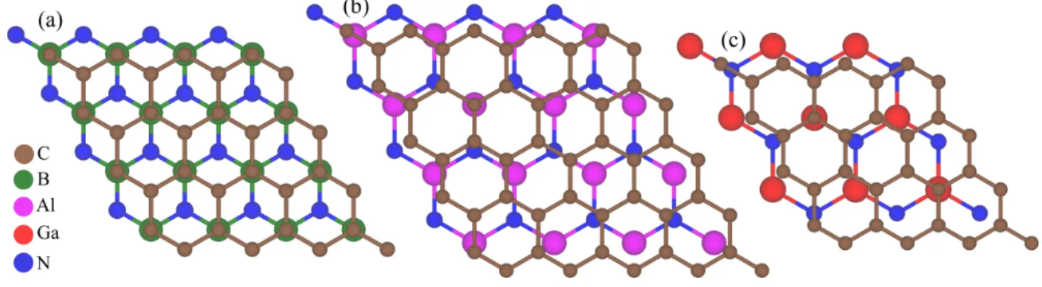
In Fig. 1 we show the supercell geometries of the graphene/hBN, graphene/hAlN, and graphene/hGaN heterostructures. The lattice constant of graphene 68 is a = 2.46 ˚ A, the one of hBN 69 is a = 2.504 ˚ A, the one of hAlN 36 is a = 3.12 ˚ A, and the one of hGaN 36 is a = 3.25 ˚ A, which we slightly adapt (straining the lat- tices by less than 2%) for the periodic first-principles cal- culations. For the graphene/hBN structure, we consider 4 × 4 (5 × 5) supercells of graphene and hBN, both with a lattice constant of a = 2.4820 ˚ A, and we use the most energetically favorable stacking for these commensurate lattices 5 . In the case of graphene on hGaN, we place a 4 × 4 graphene unit cell, with a compressed lattice con- stant of a = 2.4486 ˚ A, on a 3 × 3 hexagonal hGaN unit cell, with a stretched lattice constant of a = 3.2649 ˚ A 36 . For graphene on hAlN, we place a 5 × 5 graphene unit cell, with a stretched lattice constant of a = 2.4816 ˚ A, on a 4 × 4 hexagonal hAlN unit cell, with a compressed lattice constant of a = 3.102 ˚ A 35,36,47 .
First-principles calculations are performed with a full potential linearized augmented plane wave (FLAPW) code based on density functional theory (DFT), as im- plemented in WIEN2k 70 . Exchange-correlation effects are treated with the generalized-gradient approximation (GGA) 71 , including a dispersion correction 72 .
For graphene/hGaN, we use a k-point grid of 18 ×18 × 1, and the values of the Muffin-tin radii are R C = 1.33 for C atoms, R Ga = 1.90 for Ga atoms, and R N = 1.64 for N atoms, with the plane wave cutoff parame- ter RK MAX = 4.7. For graphene/hAlN, we use a k- point grid of 12 × 12 × 1, and the Muffin-tin radii are R C = 1.35 for C atoms, R Al = 1.72 for Al atoms, and R N = 1.64 for N atoms, with the plane wave cutoff pa- rameter RK MAX = 4.2. We consider only the stack- ing configurations shown in Fig. 1. For these two het- erostructures we vary the distance between the graphene and hXN layers to find the lowest energy separation.
When we then consider graphene encapsulated in hAlN
FIG. 1. (Color online) Top view of the supercell geometry of (a) graphene on hBN (4 × 4), (b) graphene on hAlN, and (c) graphene on hGaN. Different colors correspond to different atom types.
−3
−2
−1 0 1 2 3 4
Γ M K Γ
E − E
F[eV]
(a) grp
hBN
−3
−2
−1 0 1 2 3 4
Γ M K Γ
E − E
F[eV]
(b) grp
hAlN
−3
−2
−1 0 1 2 3 4
Γ M K Γ
E − E
F[eV]
(c) grp
hGaN
ε
1VBε
VB2ε
CB1ε
2CBFIG. 2. (Color online) Calculated band structures of graphene on (a) hBN, (b) hAlN, and (c) hGaN. Bands corresponding to different layers (graphene, hBN, hAlN, hGaN) are plotted in different colors (black, green, purple, red). The inset in (a) shows a sketch of the low energy dispersion close to the K point. Due to the presence of the substrate, graphene’s low energy bands are split into four states ε
CB/VB1/2, with a band gap.
or hGaN, we use these interlayer distances. For the en- capsulated structures, a second hAlN (hGaN) layer is added on top of the graphene/hAlN (graphene/hGaN) stack, and we use an AA 0 stacking of the two hAlN (hGaN) layers with graphene sandwiched between. In order to avoid interactions between periodic images of our slab geometries, we add a vacuum of at least 24 ˚ A in the z direction for all structures we consider.
Graphene/hBN heterostructures were already exten- sively discussed in Ref. 5. For purposes of comparison, we consider here 4 × 4 (5 × 5) graphene/hBN supercells, using a k-point grid of 18 × 18 × 1 (12 × 12 × 1) and an interlayer distance of d = 3.48 ˚ A. The Muffin-tin radii are R C = 1.35 for C atoms, R B = 1.28 for B atoms, and R N = 1.41 for N atoms, with the plane wave cutoff parameter RK MAX = 4.7 (4.2).
We also consider asymmetric hBN/graphene/hGaN and hBN/graphene/hAlN sandwich structures. In these
cases, we take the geometries for graphene/hAlN and graphene/hGaN with their energetically most favorable interlayer distances and place another hBN layer above graphene at a distance of d = 3.48 ˚ A. The in-plane lat- tice constant of hBN is adapted to that of graphene. For the sandwich structure including hGaN (hAlN), we use a k-point grid of 18 × 18 × 1 (12 × 12 × 1). The Muffin- tin radii are R C = 1.33 (1.35) for C atoms, R B = 1.26 (1.28) for B atoms, R N = 1.39 (1.41) for N atoms, and R Ga = 1.90 (R Al = 1.72) for Ga (Al) atoms, with the plane wave cutoff parameter RK MAX = 4.7 (4.2).
III. MODEL HAMILTONIAN
The band structure of proximitized graphene can
be modeled by symmetry-derived Hamiltonians 73 . For
graphene in heterostructues with C 3v symmetry, the ef-
fective low energy Hamiltonian is
H = H 0 + H ∆ + H I + H R + H PIA , (1) H 0 = ~ v F (τ k x σ x − k y σ y ) ⊗ s 0 , (2)
H ∆ = ∆σ z ⊗ s 0 , (3)
H I = τ(λ A I σ + + λ B I σ − ) ⊗ s z , (4) H R = −λ R (τ σ x ⊗ s y + σ y ⊗ s x ), (5) H PIA = a(λ A PIA σ + − λ B PIA σ − ) ⊗ (k x s y − k y s x ). (6) Here v F is the Fermi velocity and the in-plane wave vector components k x and k y are measured from ±K, corresponding to the valley index τ = ±1. The Pauli spin matrices are s i , acting on spin space (↑, ↓), and σ i are pseudospin matrices, acting on sublattice space (C A , C B ), with i = {0, x, y, z} and σ ± = 1 2 (σ z ± σ 0 ).
The lattice constant of graphene is a and the staggered sublattice potential gap is ∆. The parameters λ A I and λ B I describe the sublattice-resolved intrinsic SOC, λ R
stands for the Rashba SOC, and λ A PIA and λ B PIA are for the sublattice-resolved pseudospin-inversion asymmetry (PIA) SOC. The basis states are |Ψ A , ↑i, |Ψ A , ↓i, |Ψ B , ↑i, and |Ψ B , ↓i, resulting in four eigenvalues ε CB/VB 1/2 .
IV. FIRST-PRINCIPLES AND FIT RESULTS In Fig. 2, we show the calculated band structures of graphene on hBN, hAlN, and hGaN. We find that the Dirac bands are always preserved and are located inside the band gap of the substrate. The low energy bands of graphene are split into four states ε CB/VB 1/2 with a band gap, as shown in the inset in Fig. 2(a), which is caused by the pseudospin symmetry breaking and the proximity- induced SOC.
A. Low energy bands
In Fig. 3 we show the low energy band properties of the graphene/hAlN stack. We find perfect agreement of the band structure, band splittings and spin expectation values with the first-principles data, in the vicinity of the K point. In Fig. 3(a) we show a zoom to the low energy bands with a fit to our low energy model Hamil- tonian. The splittings, shown in Fig. 3(b), are around 30 µeV near the K point, and are of the same order as for graphene on hBN 5 . The s x and s y spin expectation values show a clear signature of Rashba SOC, while the s z expectation value sharply decays away from the K point, see Fig. 3(c-e). In Fig. 4 we show the low energy band properties of the graphene/hGaN stack. The overall re- sults are very similar, except that the band splittings are much larger, around 120 µeV near the K point. The model is also in perfect agreement with the calculated bands.
The fit parameters are summarized in Table I. We find that hGaN induces larger band splittings in graphene
−0.5 0 0.5
M ← K → Γ
1 0 1
E − E
F[meV]
k [10
−4/Å]
Model DFT
0 10 20 30 40
M ← K → Γ
splitting [ µ eV]
cond val
−1
−0.5 0.5 0 1
M ← K → Γ
< s
x>
−1
−0.5 0.5 0 1
M ← K → Γ
< s
y>
−1
−0.5 0.5 0 1
M ← K → Γ
< s
z>
(a)
(b)
(c)
(d)
(e)
FIG. 3. (Color online) Calculated low energy band properties of graphene on hAlN in the vicinity of the K point with an in- terlayer distance of 3.48 ˚ A. (a) First-principles band structure (symbols) with a fit to the model Hamiltonian (solid line). (b) The splitting of conduction band ∆E
CB(blue) and valence band ∆E
VB(red) close to the K point and calculated model results. (c)-(e) The spin expectation values of the bands ε
VB2and ε
CB1and comparison to the model results.
−1 0 1
M ← K → Γ
2 1 0 1 2
E − E
F[meV]
k [10
−4/Å]
Model DFT
30 60 90 120
M ← K → Γ
splitting [ µ eV]
cond val
−1
−0.5 0.5 0 1
M ← K → Γ
< s
x>
−1
−0.5 0.5 0 1
M ← K → Γ
< s
y>
−1
−0.5 0.5 0 1
M ← K → Γ
< s
z>
(a)
(b)
(c)
(d)
(e)
FIG. 4. (Color online) Calculated low energy band properties of graphene on hGaN in the vicinity of the K point with an in- terlayer distance of 3.48 ˚ A. (a) First-principles band structure (symbols) with a fit to the model Hamiltonian (solid line). (b) The splitting of conduction band ∆E
CB(blue) and valence band ∆E
VB(red) close to the K point and calculated model results. (c)-(e) The spin expectation values of the bands ε
VB2and ε
CB1and comparison to the model results.
than hAlN, as reflected in the 4-times larger Rashba pa-
rameter. The origin of this sizeable Rashba coupling is
the deformation of C p z orbitals along the z direction 74
(see Appendix), being much more pronounced in the
hGaN case compared to the other substrates. In Ta-
ble I we also summarize fit results for the graphene/hBN
stacks (4 × 4 and 5 × 5 supercells). Both give similar re-
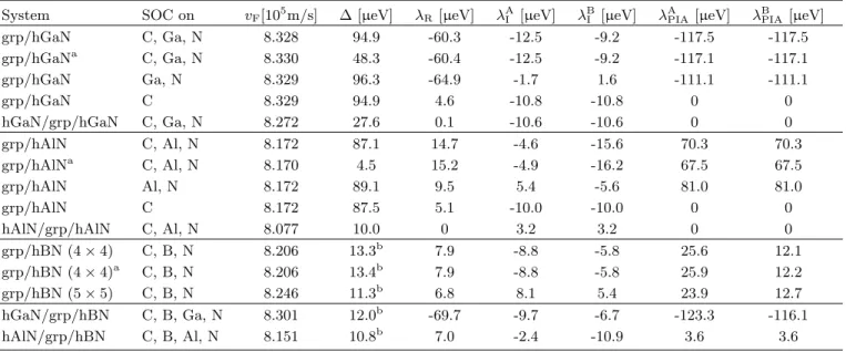
TABLE I. Summary of the fit parameters of Hamiltonian H, for graphene/hBN, graphene/hGaN, and graphene/hAlN systems with interlayer distances of 3.48 ˚ A. We have artificially turned off SOC on N, Al, Ga, or C atoms, to resolve the contributions of individual atoms to the band splittings. The fit parameters are the Fermi velocity v
F, gap parameter ∆, Rashba SOC parameter λ
R, intrinsic SOC parameters λ
AIand λ
BI, and PIA SOC parameters λ
APIAand λ
BPIAfor sublattices A and B.
System SOC on v
F[10
5m/s] ∆ [µeV] λ
R[µeV] λ
AI[µeV] λ
BI[µeV] λ
APIA[µeV] λ
BPIA[µeV]
grp/hGaN C, Ga, N 8.328 94.9 -60.3 -12.5 -9.2 -117.5 -117.5
grp/hGaN
aC, Ga, N 8.330 48.3 -60.4 -12.5 -9.2 -117.1 -117.1
grp/hGaN Ga, N 8.329 96.3 -64.9 -1.7 1.6 -111.1 -111.1
grp/hGaN C 8.329 94.9 4.6 -10.8 -10.8 0 0
hGaN/grp/hGaN C, Ga, N 8.272 27.6 0.1 -10.6 -10.6 0 0
grp/hAlN C, Al, N 8.172 87.1 14.7 -4.6 -15.6 70.3 70.3
grp/hAlN
aC, Al, N 8.170 4.5 15.2 -4.9 -16.2 67.5 67.5
grp/hAlN Al, N 8.172 89.1 9.5 5.4 -5.6 81.0 81.0
grp/hAlN C 8.172 87.5 5.1 -10.0 -10.0 0 0
hAlN/grp/hAlN C, Al, N 8.077 10.0 0 3.2 3.2 0 0
grp/hBN (4 × 4) C, B, N 8.206 13.3
b7.9 -8.8 -5.8 25.6 12.1
grp/hBN (4 × 4)
aC, B, N 8.206 13.4
b7.9 -8.8 -5.8 25.9 12.2
grp/hBN (5 × 5) C, B, N 8.246 11.3
b6.8 8.1 5.4 23.9 12.7
hGaN/grp/hBN C, B, Ga, N 8.301 12.0
b-69.7 -9.7 -6.7 -123.3 -116.1
hAlN/grp/hBN C, B, Al, N 8.151 10.8
b7.0 -2.4 -10.9 3.6 3.6
a
The rippled structure from the relaxation of internal atomic positions.
b
For the graphene/hBN structures, the sublattice-symmetry breaking is much larger (see Ref. 5) and the parameter ∆ is given in meV.
sults, as already found in Ref. 5, which further validates our DFT calculations. In contrast to the graphene/hAlN and graphene/hGaN stacks, the staggered potential gap parameter ∆ is much larger in the graphene/hBN case.
In the case of hBN, the individual graphene sublattices (A and B) are perfectly aligned above the boron and hol- low positions of hBN, see Fig. 1(a), leading to a strong sublattice-symmetry breaking and a large staggered po- tential gap. In contrast, for hGaN and hAlN the sub- lattice atoms of graphene are nearly arbitrarily aligned above the substrates, see Fig. 1(b,c), and very little sub- lattice asymmetry arises.
We additionally calculated the low energy band struc- tures when SOC is artificially turned off in the nitrogen, gallium, aluminum or carbon atoms. The fit parameters for these situations are also given in Table I. From these fits we can resolve the atomic contributions to the SOC parameters induced solely by the substrate. When SOC of the substrate is neglected, we recover the intrinsic SOC of pristine graphene 74 , and strongly reduce the Rashba and PIA contributions to the band splittings.
B. Distance Study
In Fig. 5, we show the evolution of the fit param- eters for graphene/hAlN and graphene/hGaN as we vary the interlayer distance, similar to Ref. 5 for the graphene/hBN stack. We find that the total energy of the systems are minimized for interlayer distances of 3.48 ˚ A, in agreement with literature showing weak
vdW bonding 62 . Additionally, we find that the Rashba and PIA parameters decrease with increasing distance, while the intrinsic SOC parameters converge towards the known value of about 10 µeV for pristine graphene 74 . The different Fermi velocities for the two systems can be attributed to the different graphene lattice constants used in the heterostructure calculations, which affects the magnitude of the nearest-neighbor hopping integral.
C. Encapsulated Structures
In the symmetric encapsulated graphene het- erostructures, namely hAlN/graphene/hAlN and hGaN/graphene/hGaN, we find that, compared to the non-encapsulated cases, Rashba SOC is strongly sup- pressed because inversion symmetry is nearly restored, as shown in Table I. Thus, the encapsulated geometries should in principle lead to larger spin lifetimes, as is the case for graphene/hBN structures 5 . In the case of the hBN/graphene/hGaN and hBN/graphene/hAlN structures, the fit parameters are also summarized in Table I and result from an interplay between the different top and bottom encapsulation layers. The hBN layer significantly enhances the orbital gap parameter
∆ due to commensurability with the graphene lattice
and the resulting sublattice-symmetry breaking. In the
case of hBN/graphene/hGaN, the SOC parameters are
similar to the non-encapsulated graphene/hGaN case,
as if the hBN layer would have no effect. In particular,
the Rashba and PIA SOC parameters have roughly the
0 200 400 600
3.1 3.2 3.3 3.4 3.5 E
tot[meV]
distance [Å]
(a)
hGaN hAlN
7.6 7.8 8 8.2 8.4
3.1 3.2 3.3 3.4 3.5 v
F/10
5[m/s]
distance [Å]
(b)
0 0.1 0.2 0.3 0.4 0.5
3.1 3.2 3.3 3.4 3.5
∆ [meV]
distance [Å]
(c)
−200 −150
−100 −50 50 0
3.1 3.2 3.3 3.4 3.5 λ
R[µ eV]
distance [Å]
(d)
−15 −10 −5 10 0 5
3.1 3.2 3.3 3.4 3.5 λ
IA[µ eV]
distance [Å]
(e)
−30
−25
−20
−15
−10 −5
3.1 3.2 3.3 3.4 3.5 λ
IB[µ eV]
distance [Å]
(f)
−400
−200 0 200 400
3.1 3.2 3.3 3.4 3.5 λ
PIAA[µ eV]
distance [Å]
(g)
−400
−200 0 200 400
3.1 3.2 3.3 3.4 3.5 λ
PIAB[µ eV]
distance [Å]
(h) 0
200 400 600
3.1 3.2 3.3 3.4 3.5
tot
[ ]
distance [Å]
(a)
hGaN hAlN
7.6 7.8 8 8.2 8.4
3.1 3.2 3.3 3.4 3.5 v
F/10 [m/s]
distance [Å]
(b)
0 0.1 0.2 0.3 0.4 0.5
3.1 3.2 3.3 3.4 3.5
∆ [meV]
distance [Å]
c)
−200 −150
−100 −50 50 0
3.1 3.2 3.3 3.4 3.5
R
[µ ]
distance [Å]
d)
−15 −10 −5 10 0 5
3.1 3.2 3.3 3.4 3.5 λ
IA[µ eV]
distance [Å]
(e)
−30
−25
−20
−15
−10 −5
3.1 3.2 3.3 3.4 3.5 λ
IB[µ eV]
distance [Å]
(f)
−400
−200 0 200 400
3.1 3.2 3.3 3.4 3.5 λ
PIAA[µ eV]
distance [Å]
(g)
−400
−200 0 200 400
3.1 3.2 3.3 3.4 3.5 λ
PIAB[µ eV]
distance [Å]
(h)
FIG. 5. (Color online) Fit parameters as a function of distance between graphene and hAlN or hGaN. (a) Total energy, (b) Fermi velocity v
F(c) gap parameter ∆, (d) Rashba SOC pa- rameter λ
R, (e) intrinsic SOC parameter λ
AIfor sublattice A, (f) intrinsic SOC parameter λ
BIfor sublattice B, (g) PIA SOC parameter λ
APIAfor sublattice A, and (h) PIA SOC parameter λ
BPIAfor sublattice B.
same values. In contrast, for the hBN/graphene/hAlN structure, the formerly large PIA parameters from the non-encapsulated graphene/hAlN case are now strongly suppressed, while the intrinsic and Rashba SOC are of similar magnitude.
D. Electric Field Effects
Gating can be used to tune the SOC, especially the Rashba SOC, in the Dirac bands of graphene 5,74 . Tun- ing the SOC can have a significant impact on spin trans- port and relaxation properties. Consequently, gating is a potentially efficient control knob in experimental studies. Here we apply a transverse electric field, mod- eled by a sawtooth potential, across graphene/hAlN and graphene/hGaN heterostructures for a fixed interlayer distance of 3.48 ˚ A. The results are summarized in Fig. 6.
Indeed, most of the parameters can be tuned by the field. Especially in the case of hGaN, the tunability of the Rashba, intrinsic, and PIA SOC parameters is giant within our considered field limits. Tuning the field from
−3 to 3 V/nm, we find that the Rashba SOC can be enhanced in magnitude from about 40 to 90 µeV. The intrinsic SOC parameter for sublattice A (B) decreases (increases) in magnitude, while both PIA parameters can
−0.5
−0.25 0
−2 0 2
(a)
(b)
(c)
(d)
(e)
(f)
(g)
(h) EVBE− EF[meV]
electric field [V/nm]
hGaNhAlN
8.18 8.2 8.38.4
−2 0 2
vF/105[m/s]
electric field [V/nm]
80 90 100 110
−2 0 2
∆
[µ
eV]electric field [V/nm]
−75−50
−25250
−2 0 2
λR[
µ
eV]electric field [V/nm]
−15
−10
−5
−2 0 2
λIA[
µ
eV]electric field [V/nm]
−15
−10
−5
−2 0 2
λIB[
µ
eV]electric field [V/nm]
−200
−1001000
−2 0 2
λPIAA[
µ
eV]electric field [V/nm]
−200
−1001000
−2 0 2
λPIAB[
µ
eV]electric field [V/nm]
FIG. 6. (Color online) Fit parameters as a function of the transverse electric field for graphene/hAlN and graphene/hGaN at fixed interlayer distances of 3.48 ˚ A.
(a) The valence band edge with respect to the Fermi level, (b) the Fermi velocity v
F, (c) gap parameter ∆, (d) Rashba SOC parameter λ
R, (e) intrinsic SOC parameter λ
AIfor sub- lattice A, (f) intrinsic SOC parameter λ
BIfor sublattice B, (g) PIA SOC parameter λ
APIAfor sublattice A, and (h) PIA SOC parameter λ
BPIAfor sublattice B.
be drastically enhanced by a factor of 2 when the field is tuned from negative to positive values. In the case of hAlN as the substrate, the electric field tunability is somewhat similar, but not as pronounced as in the case of hGaN. However, the PIA couplings show also a strong tunability ranging from 40 to 170 µeV within our electric field limits.
E. Rippling Effects
So far, we only considered flat monolayers stacked on
top of each other, with fixed interlayer distances. In ex-
periment, the layers are typically not completely flat and
rippling occurs due to imperfections and impurities. How
does rippling affect the proximity-induced SOC? The
starting point are the graphene/hXN heterostructures
with the energetically most favorable interlayer distance
of 3.48 ˚ A, to which we apply the force relaxation 75–77
implemented in the WIEN2k code. Thereby, we deter-
mine the equilibrium positions of all atoms by minimiz-
ing the forces on the nuclei, while respecting the C 3v -
symmetry of the heterostructures. When all forces are
below 0.5 mRy/bohr, we continue to calculate the low
energy bands and apply the model Hamiltonian fit rou-
tine. The fit results are summarized in Table I.
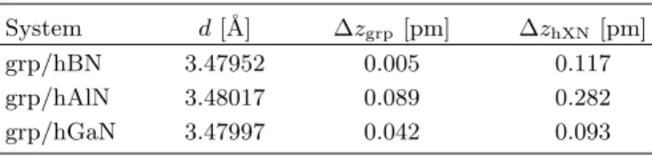
After relaxation of a given graphene/hXN heterostruc- ture, we also calculate the mean values, ¯ z, and the standard deviations, ∆z, of the z coordinates of the atoms belonging to the individual monolayers. From the mean values, we calculate the average interlayer distance, d = ¯ z grp − z ¯ hXN , between graphene and hXN, while the standard deviations represent the amount of rippling of the layers. The results are summarized in Table II.
Overall, we find that the average interlayer distances are barely affected and the individual monolayers are still nearly flat with a maximum rippling below 1 pm. Com- paring the fit parameters in Table I, for the flat and rip- pled structures, we find that mainly the staggered po- tential gap ∆ is affected, while the SOC parameters stay nearly the same. In the case of hGaN, ∆ is about twice as large in the flat structure compared to the rippled one. For hAlN, the effect is even more drastic, since the rippled structure nearly leads to a vanishing sublattice asymmetry in graphene, while the flat structure has a 20-times larger asymmetry, as reflected in the parameter
∆.
TABLE II. The calculated average interlayer distances, d, and the ripplings, ∆z, of the monolayers, of the graphene/hXN heterostructures after relaxation of internal forces.
System d [˚ A] ∆z
grp[pm] ∆z
hXN[pm]
grp/hBN 3.47952 0.005 0.117
grp/hAlN 3.48017 0.089 0.282
grp/hGaN 3.47997 0.042 0.093
V. SPIN RELAXATION A. Model and Numerical Approach
We now use a combination of modeling and numeri- cal simulations to predict the nature and magnitude of spin relaxation in graphene/hXN heterostructures. To numerically simulate spin transport, we use a real-space time-dependent approach that has been employed for the study of electrical and spin transport in a wide va- riety of disordered materials 78 . We initialize a spin- polarized random-phase state in a 500×500 nm 2 sam- ple of graphene, and we evolve it in time using an effi- cient Chebyshev expansion of the time evolution opera- tor. At each time step we calculate the spin polarization s i (E, t) and the mean-square displacement ∆X 2 (E, t) of the state as a function of the Fermi energy E. The energy-dependent spin lifetime τ s,i (E) is then extracted by fitting the spin polarization to an exponential de- cay, s i (E, t) = exp(−t/τ s,i (E)). We also calculate the momentum relaxation time τ p (E) = 2D(E)/v 2 F , where D(E) = max
t
1
2 d
dt ∆X 2 (E, t) is the semiclassical diffu-
sion coefficient.
To induce charge scattering and thus spin relaxation in our simulations, we include a random distribution of Gaussian-shaped electrostatic impurities which are meant to represent the impact of charges trapped in the substrate below graphene 79 . The electrostatic po- tential at each atomic site i is then given by i = P
j
V j exp(−|~ r i − ~ r j | 2 /2ξ 2 ), where ~ r i is the position of each carbon atom, ~ r j is the position of each impurity, ξ is the width of each impurity, and the height V j of each impurity is randomly distributed in [−V, V ]. Here we use V = 2.8 eV, ξ = √
3a, and an impurity density of 0.1%. This choice of parameters leads to a charge mo- bility around 1000 cm 2 /Vs and intervalley scattering in the range of τ iv ≈ (10 − 60)τ p . For each graphene/hXN heterostructure, we convert the continuum Hamiltonian of Eq. (1) to a real-space tight-binding form and use the first set of paramemeters in Table I.
In our numerical simulations we have only considered the graphene/hGaN heterostructure, as the others have lower SOC, putting their spin lifetimes outside the range of what we can simulate numerically. Thus, to explain the features seen in our simulations and to make predic- tions for the hAlN and hBN heterostructures, we now de- scribe a simple and transparent model of spin relaxation in these systems. We start by assuming the only source of spin relaxation is from the SOC parameters defined in Eq. (1), and not from extrinsic sources such as ripples or magnetic impurities 80,81 . There are two traditional spin relaxation mechanisms driven by uniform SOC, namely the Elliott-Yafet (EY) and the D’yakonov-Perel’ (DP) mechanisms 82–84 . The numerical simulations show a neg- ligible EY contribution and thus we focus solely on the DP mechanism. The spin relaxation rates in graphene are then given by 5,85,86
τ s,x −1 = τ p hω y 2 i + τ iv hω 2 z i,
τ s,y −1 = τ p hω x 2 i + τ iv hω z 2 i, (7) τ s,z −1 = τ p hω x 2 + ω 2 y i,
where τ s,x/y are the lifetimes of spins pointing in the graphene plane, τ s,z is the out-of-plane spin lifetime, τ p
is the momentum relaxation time, τ iv is the intervalley scattering time, and ω i are the components of the effec- tive magnetic field induced by SOC. As we will see below, the z-component of the effective magnetic field has oppo- site sign in the ±K valleys and thus drives spin relaxation through intervalley scattering, while the in-plane compo- nents depend on the direction of electron momentum and thus are connected to τ p .
The effective magnetic field can be written as (see Ap-
pendix)
~ 2 ω x =
±λ R + akλ + PIA
+ g k (k)
· sin(−θ),
~ 2 ω y =
±λ R + akλ + PIA
+ g k (k)
· cos(θ),
~
2 ω z = [λ VZ + g z (k)] · τ, (8) where λ + PIA = (λ A PIA + λ B PIA )/2 gives rise to a k-linear spin splitting similar to Rashba SOC in traditional 2D electron gases, λ VZ = (λ A I − λ B I )/2 is the valley-Zeeman SOC, and θ denotes the direction of electron momentum k in the graphene plane. The +(−) sign in ω x/y is for the valence (conduction) band, and thus a strong PIA SOC can induce electron-hole asymmetry in the spin relax- ation. Note that ω z is proportional to τ and thus has op- posite sign in opposite valleys, as mentioned above. The second terms in the brackets, g k/z (k), represent higher- order terms in the effective magnetic field. These are large near the graphene Dirac point ( ~ v F k . ∆, λ i ) and decay as ∼1/k at higher energies.
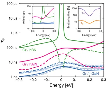
B. Single-Sided Heterostructures
The numerical results for the graphene/hGaN het- erostructure are shown as the symbols in Fig. 7. The right inset shows the momentum relaxation time, which ranges from 6 to 20 fs, and the intervalley scattering time, which ranges from 75 fs to 1 ps. The blue tri- angles (squares) in the main panel show the in-plane (out-of-plane) spin lifetime as a function of Fermi en- ergy. Lifetimes are between 1 and 10 ns, with a max- imum around the charge neutrality point and a slight electron-hole asymmetry. The spin lifetime anisotropy, defined as the ratio of out-of-plane to in-plane spin life- time, ζ ≡ τ s,z /τ s,x , is shown as the blue circles in the left inset. The anisotropy is nearly 1/2 over the entire energy range, indicating that spin relaxation is driven by the DP mechanism with a dominant Rashba+PIA SOC.
The peak in the spin lifetime around E = 0, correspond- ing to the dip in τ p at the same point, is also indicative of the DP mechanism.
To better understand these results, we now turn to the model of Eqs. (7)-(8). We first examine the cases of graphene/hAlN and graphene/hGaN, for which all en- ergies in Table I are small, less than 100 µeV (for PIA SOC, the relevant energy scale is akλ PIA ). If we consider spin transport near room temperature (k B T ≈ 26 meV), then the g k/z (k) terms in Eq. (8) are smeared out by the large thermal broadening and only the first terms in the brackets are responsible for spin transport. The in-plane
(QHUJ\>H9@
QV QV QV V V V
s
*UK*D1
*UK$O1
*UK%1
(QHUJ\>H9@
$QLVRWURS\
(QHUJ\>H9@
6FDWWHULQJWLPH>IV@
p iv
FIG. 7. (Color online) Predicted spin lifetime in graphene/hXN heterostructures. The solid (dashed) lines show the out-of-plane (in-plane) spin lifetimes calculated from Eqs. (7)-(10). The symbols show the spin lifetime from nu- merical simulations of graphene/hGaN. The left inset shows the spin lifetime anisotropy for each heterostructure, and the right inset shows the momentum relaxation time and inter- valley scattering time calculated from numerical simulations.
and out-of-plane spin relaxation rates are then given by τ s,x −1 = τ s,y −1 = 1
2 τ s,z −1 + 2
~ λ VZ
2
τ iv ,
τ s,z −1 = 2
~ ±λ R + akλ + PIA 2
τ p , (9) the same as what was previously derived for graphene/TMDC heterostructures, in which strong valley-Zeeman SOC coupled with intervalley scattering leads to large values of spin lifetime anisotropy 85,86 . Plugging the parameters from Table I and the values of τ p and τ iv from the numerical simulations into Eq. (9), we obtain spin lifetimes for graphene/GaN that match very well with the numerical simulations, as shown by the blue lines in Fig. 7. The spin lifetime anisotropy of ζ ≈ 1/2 also matches very well, confirming the dominance of Rashba+PIA over valley-Zeeman SOC.
The red lines in Fig. 7 show the expected spin lifetimes for graphene/AlN. Here the Rashba SOC is somewhat smaller, allowing the PIA SOC to play a more dominant role and resulting in significant electron-hole asymmetry.
In particular, for positive energies the PIA cancels out the Rashba SOC, which enhances the out-of-plane spin lifetime. Meanwhile, the in-plane spin lifetime is sup- pressed by an enhanced contribution from valley-Zeeman SOC, leading to large spin lifetime anisotropy. For neg- ative energies, PIA augments the Rashba SOC and the anisotropy is reduced.
Now we consider the case of spin relaxation in
graphene/hBN. In this system the staggered sublattice
potential ∆ is large, opening a band gap on the order of the thermal broadening, and thus the higher-order terms in Eq. (8) cannot be ignored. These terms are compli- cated expressions of the various parameters in the Hamil- tonian (see Appendix), but for the values given in Table I they are well captured (to within 1%) by
g k (k) = ∆ 2 λ VB + 2∆ε − PIA ε ∆ k ε ∆ k 2 ,
g z (k) = ∆ 2 λ VZ + 2∆λ I ε ∆ k
ε ∆ k 2 , (10)
where λ VB = λ R + akλ + PIA , ε − PIA = ak(λ A PIA − λ B PIA )/2, λ I = (λ A I +λ B I )/2 is the intrinsic or Kane-Mele SOC, and ε ∆ k = ~ v F k + p
( ~ v F k) 2 + ∆ 2 . Equation (10) was derived for spin transport in the conduction band, but similar terms apply to the valence band by replacing λ R → −λ R
and ε ∆ k → −ε ∆ k .
In the high-energy limit, the terms in Eq. (10) disap- pear and the spin lifetime is described by Eq. (9). How- ever, as the Fermi energy approaches the band edges (k → 0), ω x/y → 0 and ω z → 2(λ I + λ VZ ). Thus, the out-of-plane spin lifetime diverges while the in-plane spin lifetime remains finite, leading to a giant spin lifetime anisotropy around the charge neutrality point. This be- havior is shown as the green lines in Fig. 7, and corrob- orates previous predictions of spin lifetime anisotropy in these systems 5 . These results indicate that a large spin lifetime anisotropy should be visible around the charge neutrality point in graphene heterostructures with a large staggered sublattice potential, even if the SOC is small.
C. Electric Field Dependence
As shown in Fig. 6 above, an external electric field can be used to efficiently tune the various spin-orbit pa- rameters in the graphene/hGaN and graphene/hAlN het- erostructures. We plot the resulting impact on the spin lifetime anisotropy in Fig. 8. For positive E-fields, the anisotropy in graphene/hGaN remains around 1/2, as the Rashba SOC is the dominant term. For negative fields, the Rashba SOC strength is reduced, valley-Zeeman SOC begins to play a role, and a modest anisotropy appears, reaching a value of ζ ≈ 3 at high doping levels.
In contrast, the Rashba SOC in graphene/hAlN is somewhat weaker and has the opposite sign. The re- sult is that the spin lifetime anisotropy is significantly larger (note the log color scale for this system), and is maximized at positive E-fields, where the magnitude of Rashba SOC is smallest. Although the magnitude of the anisotropy is quite different, it is evident that in both systems it is tunable via external field and doping.
(QHUJ\>H9@
(ILHOG>9QP@
*UK$O1
(ILHOG>9QP@
*UK*D1
$QLVRWURS\
FIG. 8. (Color online) Spin lifetime anisotropy in graphene/hGaN and graphene/hAlN heterostructures. Re- sults for graphene/hGaN were calculated numerically, while those for graphene/hAlN were derived from Eq. (9).
D. Double-Sided Heterostructures
Beyond an external electric field, spin transport prop- erties may be further tuned by sandwiching graphene between different hXN layers. For example, by placing hBN on one side of graphene and hGaN or hAlN on the other side, one can realize a system that combines the SOC properties of graphene/hGaN or graphene/hAlN, but with the large orbital gap of graphene/hBN. This can be seen by examining the final two rows of Table I.
Spin lifetimes for the hBN/graphene/hGaN and hBN/graphene/hAlN systems are shown in Fig. 9(a), with solid (dashed) lines denoting out-of-plane (in-plane) lifetime. The spin lifetime anisotropy is shown in the in- set. As expected, each system exhibits a giant anisotropy around the charge neutrality point, owing to the orbital gap induced by the hBN layer. Away from the gap, the hBN/graphene/hGaN system behaves just like the single-sided graphene/hGaN system, with an anisotropy of 1/2 resulting from the dominant Rashba SOC. Mean- while, the hBN/graphene/hAlN system exhibits large anisotropy and strong electron-hole asymmetry, similar to Fig. 7 above. Thus, these double-sided heterostruc- tures appear to behave as a “superposition” of two single- sided heterostructures, with hBN providing the orbital gap and hGaN or hAlN providing the particular nature of the SOC.
In Figs. 7 and 9(a) we have predicted spin lifetimes
ranging from 1 ns up to hundreds of ns. These large
lifetimes arise from the small SOC in these systems, but
as shown in Table I, the SOC can be further reduced
by encapsulating graphene between two identical hXN layers. In this case, the valley-Zeeman and PIA SOC disappear, and the Rashba SOC is also completely or nearly eliminated. In this situation the effective magnetic field becomes
~
2 ω x = ±λ R
1 + 2λ I /ε ∆I k
· sin(−θ),
~
2 ω y = ±λ R
1 + 2λ I /ε ∆I k
· cos(θ),
~
2 ω z = ∆
2λ I /ε ∆I k
· τ, (11)
where ε ∆I k = ~ v F k + p
( ~ v F k) 2 + (∆ + λ I ) 2 . In Fig. 9(b) we plot the spin lifetimes for graphene encapsulated by hGaN or hAlN. Owing to the small SOC, all spin life- times are extremely large; around one millisecond for GaN and up to several seconds for AlN. In these sys- tems, ω z strongly increases at low energies, leading to a sharp decrease of the in-plane spin lifetime and thus a large anisotropy around the charge neutrality point for the GaN system. For the AlN system, the out-of-plane spin lifetime is infinite due to the absence of Rashba SOC and thus is not pictured.
QV QV QV V V V
s
D
K%1*UK*D1 K%1*UK$O1
(QHUJ\>H9@
$QLVRWURS\
(QHUJ\>H9@
QV V PV V V
s
E
K*D1*UK*D1 K$O1*UK$O1
(QHUJ\>H9@
$QLVRWURS\
FIG. 9. (Color online) Predicted spin lifetime in (a) hBN/graphene/hXN and (b) hXN/graphene/hXN het- erostructures. The solid (dashed) lines show the out-of-plane (in-plane) spin lifetimes calculated from Eqs. (7)-(11). The insets show the corresponding spin lifetime anisotropy.
It should be noted that here we have used the same disorder as before, but in these encapsulated systems τ p
is expected to be up to 100 times higher, corresponding to a mobility around 100,000 cm 2 /Vs. This would re- duce the spin lifetimes by a factor of 100. However, even at these lifetimes other mechanisms are expected to take over spin relaxation, such as corrugations, phonons, or impurities. All of these are suppressed in encapsulated graphene, which, along with the strongly reduced SOC, make these systems highly promising for exploring the upper limits of spin tranport in 2D van der Waals het- erostructures.
VI. SUMMARY
In this work, we have considered heterostructures of graphene and the monolayer hexagonal nitride insula- tors, hBN, hAlN, and hGaN, from first principles. In the cases of graphene on hAlN and hGaN, we performed an interlayer distance study to find the energetically most favorable van der Waals gap, which is about 3.48 ˚ A. Our calculations, combined with a low energy model Hamilto- nian, reveal that graphene’s linear dispersion is well pre- served within the insulator band gap for all considered heterostructures, and the fitted model SOC parameters, describing the spin splitting of the Dirac states, are below 100 µeV for optimized interlayer distances. From the in- terlayer distance study, we also find that the fitted orbital and SOC parameters strongly depend on the distance be- tween graphene and the substrate. Overall, for the non- encapsulated structures, Rashba and PIA contributions dominate the spin splitting, while they are suppressed in the encapsulated cases where intrinsic SOC terms of maximum 10 µeV dominate. The model parameters are then used to estimate spin lifetimes in the encapsulated and non-encapsulated heterostructure systems.
With respect to spin transport and relaxation, sev- eral interesting and surprising features appear in these graphene/hXN systems. Depending on the relative strength of the parameters in the Hamiltonian, spin transport can be quite conventional, can exhibit strong electron/hole asymmetry in the lifetimes and in the spin lifetime anisotropy, or can exhibit giant anisotropy only around the charge neutrality point. This enhanced anisotropy around the charge neutrality point arises from a strong staggered sublattice potential ∆ in combina- tion with another source of SOC. This suggests that the graphene/hBN system, in which sublattice symme- try breaking can open a significant band gap, is the best candidate to observe this behavior. Meanwhile, graphene encapsulated in GaN or AlN appears to be an excellent candidate for exploring the upper limits of spin transport in 2D van der Waals heterostructures.
ACKNOWLEDGMENTS
This work was funded by the Deutsche Forschungsge-
meinschaft (DFG, German Research Foundation) SFB
1277 (Project-ID 314695032), DFG SPP 1666, DFG SPP 2244, and the European Unions Horizon 2020 re- search and innovation program under Grant No.881603 (Graphene Flagship). ICN2 is supported by the Severo Ochoa program from Spanish MINECO (grant no. SEV- 2017-0706) and funded by the CERCA Programme / Generalitat de Catalunya.
Appendix A: Derivation of Effective Magnetic Field In this Appendix we derive the complete form of the effective magnetic field, ~ ω, induced by SOC. In the ba- sis {|Ψ A , ↑i , |Ψ A , ↓i , |Ψ B , ↑i , |Ψ B , ↓i}, the Hamiltonian of Eq. (1) can be written in matrix form as
H =
∆ + τ λ A I ε k f ∗ ε A PIA ε + R ε ∗ k −∆ − τ λ B I ε − R f ∗ ε B PIA f ε A PIA ε − R ∗ ∆ − τ λ A I ε k
ε + R ∗ f ε B PIA ε ∗ k −∆ + τ λ B I
,
(A1) where ε k = ~ v F k · τe iτ θ , ε ± R = iλ R (τ ± 1), ε A,B PIA = akλ A,B PIA , and f = ie iθ . From this we want a Hamiltonian projected onto the conduction or valence bands with the form
H CB/VB = H 0 CB/VB + 1 2 ~ ~ ω · ~ s
=
"
±ε 0 0 0 ±ε 0
# + ~
2
"
ω z ω x − iω y ω x + iω y −ω z
#
. (A2) where H 0 CB/VB is the graphene Hamiltonian in the ab- sence of SOC (λ = 0) and sublattice symmetry breaking (∆ = 0), ω ~ is the effective magnetic field induced by these terms, and ~ s are the spin Pauli matrices.
When ∆ = λ = 0, the eigenstates of H can be written as
|Ψ CB , ↑i = h
1 τe −iτ θ 0 0 i T
/ √ 2,
|Ψ CB , ↓i = h
0 0 1 τe −iτ θ i T
/ √ 2,
|Ψ VB , ↑i = h
1 −τe −iτ θ 0 0 i T
/ √ 2,
|Ψ VB , ↓i = h
0 0 1 −τe −iτ θ i T / √
2, (A3)
where the CB/VB states have eigenenergy ±ε 0 =
± ~ v F k. Writing the Hamiltonian in the basis {|Ψ CB , ↑i , |Ψ CB , ↓i , |Ψ VB , ↑i , |Ψ VB , ↓i} yields
H ≡
"
H CC H CV
H VC H VV
#
= (A4)
ε 0 + τ λ VZ f ∗ λ CB ∆ + τ λ I f ∗ λ + CV f λ CB ε 0 − τ λ VZ f λ − CV ∆ − τ λ I
∆ + τ λ I f ∗ λ − CV −ε 0 + τ λ VZ f ∗ λ VB f λ + CV ∆ − τ λ I f λ VB −ε 0 − τ λ VZ
,
where λ CB = −λ R + akλ + PIA , λ VB = λ R + akλ + PIA , and λ ± CV = ε − PIA ± τ λ R . In the heterostructures with hBN,
∆ is much larger than the spin-orbit parameters and the eigenenergies of H are given by E ≈ ± p
ε 2 0 + ∆ 2 . When graphene is sandwiched by two identical hXN lay- ers, Table I indicates that VZ, Rashba, and PIA SOC disappear, and the eigenenergies of H are then given by E ≈ p
ε 2 0 + (∆ ± λ I ) 2 for the conduction band and the opposite sign for the valence band. In Figs. 7 and 9 we used the eigenenergy of the upper conduction band, but the results do not change appreciably if we use the lower conduction band instead.
We now reduce the full Schr¨ odinger equation, Hψ = Eψ, to expressions projected onto the conduction or va- lence band only,
Hψ = Eψ
⇓
"
H CC H CV H VC H VV
# "
ψ CB ψ VB
#
= E
"
ψ CB ψ VB
#
⇓
H CB ψ CB = Eψ CB H VB ψ VB = Eψ VB
where H CB ≡
H CC + H CV (E − H VV ) −1 H VC
H VB ≡
H VV + H VC (E − H CC ) −1 H CV
(A5)
Using the expressions for H CC etc. from Eq. (A4) above,
and writing H CB in the form given in Eq. (A2), we arrive
at the effective magnetic field given in Eq. (8), with the
full expressions for g k and g z in the conduction band
given in Eq. (A6) below. The expressions for the valence
band are similar, with the replacements λ VB → λ CB ,
λ R → −λ R , and ε 0 → −ε 0 . When ∆ is the dominant
term, as is the case for heterostructures involving hBN,
the effective magnetic field is well-approximated by the
expressions in Eq. (10).
g k (k) = λ VB
∆ 2 − λ 2 I − λ 2 R + ε − PIA 2
+ 2λ VZ λ I ε − PIA − ∆λ R
+ 2 (ε 0 + E) ∆ε − PIA − λ I λ R (ε 0 + E) 2 − λ 2 VZ − λ 2 VB
g z (k) = λ VZ
∆ 2 + λ 2 I − λ 2 R − ε − PIA 2
+ 2λ VB λ I ε − PIA + ∆λ R
+ 2 (ε 0 + E) ∆λ I + λ R ε − PIA
(ε 0 + E) 2 − λ 2 VZ − λ 2 VB (A6)
Appendix B: Density of States and Valence Charge Density
In order to find out more about the origin and the magnitude of the proximity-induced SOC in a specific graphene/hXN heterostructure, we calculate the density of states (DOS) and the valence charge density in an energy window of ±100 meV around the Fermi level. For this purpose, we use a denser k-point grid of 42 × 42 × 1 (36 × 36 × 1) for heterostructures with hBN and hGaN (hAlN).
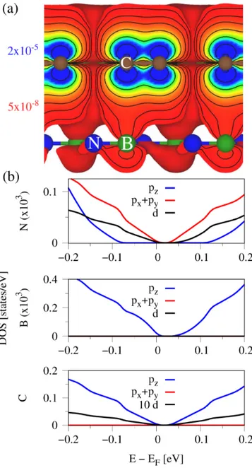
In Fig. 10, we show the calculated DOS and valence charge density for the graphene/hBN heterostructure.
From the DOS, see Fig. 10(b), we can see that mainly the p z -orbitals from B contribute near the Dirac point, while additionally N p x + p y -orbitals are present. The calculated valence charge density, see Fig. 10(a), clearly supports this picture, where a hybridization to B p z - orbitals can be directly seen. The presented results are in agreement with recent calculations of the graphene/hBN system 5 , from where we also know that N and B atoms give a significant contribution to the intrinsic SOC pa- rameters. The Rashba SOC should depend more on the deformation of C p z -orbitals along the z-axis 74 due to the hXN substrate. From the charge density plot, we cannot directly see such a deformation, hence the small Rashba SOC for the hBN case.
In order to gain some more insights, we have also cal- culated the percentage atomic composition of the total DOS at energies of ±100 meV away from the Fermi level. At 100 meV (−100 meV), the total DOS of the graphene/hBN structure is composed of 99.741% C atoms, 0.189% B atoms, and 0.069% N atoms (99.622%
C atoms, 0.291% B atoms, and 0.086% N atoms). Conse- quently, the valence band Dirac states are affected more strongly by the substrate than the conduction band Dirac states. This could be related to the fact that the |λ B I | pa- rameter, being proportional to the valence band splitting at K, deviates much stronger from the intrinsic SOC of bare graphene 74 of about 12 µeV, compared to the |λ A I | parameter, being proportional to the conduction band splitting at K. In addition, one should keep in mind that the hBN valence band edge is much closer to the Dirac point than the conduction band edge, see Fig. 2(a). All
in all, graphene is only weakly perturbed by the hBN.
Nevertheless, already such tiny substrate contributions strongly affect the SOC of the Dirac bands.
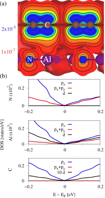
In Fig. 11, we show the calculated DOS and valence charge density for the graphene/hAlN heterostructure.
From the DOS, see Fig. 11(b), we can see that mainly the p z -orbitals from N and Al contribute for the valence Dirac bands. In contrast, for the conduction band side, also N p x + p y give a strong contribution. The calculated valence charge density, see Fig. 11(a), again supports the DOS picture. Similarly to the hBN case, a clear deforma- tion of the C p z -orbitals along the z-axis is absent, which is consistent with the rather small Rashba SOC. Similar to before, we also look at the percentage atomic com- position of the total DOS at ±100 meV away from the Fermi level. At 100 meV (−100 meV), the total DOS of the graphene/hAlN structure is composed of 98.898% C atoms, 0.083% Al atoms, and 1.018% N atoms (97.976%
C atoms, 0.164% Al atoms, and 1.860% N atoms). In contrast to the hBN case, the total N contribution is en- hanced by a factor of 10. The asymmetry in the total hAlN DOS contribution for positive and negative ener- gies is again related to the band structure, see Fig. 2(b), where the hAlN valence band edge is only about 700 meV below the Dirac point.
In Fig. 12, we show the calculated DOS and valence charge density for the graphene/hGaN heterostructure.
From the DOS, see Fig. 12(b), we find that mainly the p-orbitals from N contribute near the Dirac point, about 10-times more than for the hBN case but sim- ilar to the hAlN case. Moreover, there is some small contribution from Ga p z -orbitals in the chosen energy window around the Dirac point. The calculated valence charge density, see Fig. 12(a), clearly supports this pic- ture, where a hybridization to N p z -orbitals can be seen, which themselves couple to Ga p orbitals. In addition, the C atoms which sit above the Ga atoms display a clear deformation of the p z -orbitals along the z-axis (es- pecially looking at the green colored isovalues). This deformation should be responsible for the rather large Rashba SOC in the hGaN case, compared to the other substrates. At 100 meV (−100 meV), the total DOS of the graphene/hGaN structure is composed of 99.140% C atoms, 0.261% Ga atoms, and 0.599% N atoms (98.944%
C atoms, 0.127% Ga atoms, and 0.929% N atoms).
FIG. 10. (Color online) (a) Calculated valence charge density of the graphene/hBN heterostructure considering only states in an energy window of ±100 meV around the Fermi level.
The colors correspond to isovalues between 2 × 10
−5(blue) and 5×10
−8(red) e/˚ A
3, while the isolines range from 1×10
−3to 1 × 10
−7e/˚ A
3. (b) The atom and orbital resolved DOS.
The DOS of B and N atoms is multiplied by a factor of 10
3for comparative reasons, while for C atoms only the d-orbital contribution is multiplied by a factor of 10.
∗
klaus.zollner@physik.uni-regensburg.de
1
Banszerus, L. et al. Ultrahigh-mobility graphene devices from chemical vapor deposition on reusable copper. Sci.
Adv. 1, 1–7 (2015).
2
Petrone, N. et al. Chemical vapor deposition- derived graphene with electrical performance of exfoliated graphene. Nano Lett. 12, 2751–2756 (2012).
3
Calado, V. E. et al. Ballistic transport in graphene grown by chemical vapor deposition. Appl. Phys. Lett. 104 (2014).
4
Dr¨ ogeler, M. et al. Spin Lifetimes Exceeding 12 ns in Graphene Nonlocal Spin Valve Devices. Nano Lett. 16, 3533–3539 (2016).
5
Zollner, K., Gmitra, M. & Fabian, J. Heterostructures of
FIG. 11. (Color online) (a) Calculated valence charge density of the graphene/hAlN heterostructure considering only states in an energy window of ±100 meV around the Fermi level.
The colors correspond to isovalues between 2 × 10
−5(blue) and 1×10
−7(red) e/˚ A
3, while the isolines range from 1×10
−3to 1 × 10
−7e/˚ A
3. (b) The atom and orbital resolved DOS.
The DOS of Al (N) atoms is multiplied by a factor of 10
3(10
2) for comparative reasons, while for C atoms only the d-orbital contribution is multiplied by a factor of 10.
graphene and hBN: Electronic, spin-orbit, and spin relax- ation properties from first principles. Phys. Rev. B 99, 125151 (2019).
6
Roche, S. et al. Graphene spintronics: the European Flag- ship perspective. 2D Mater. 2, 030202 (2015).
7
Kamalakar, M. V., Dankert, A., Bergsten, J., Ive, T. &
Dash, S. P. Spintronics with graphene-hexagonal boron
FIG. 12. (Color online) (a) Calculated valence charge density of the graphene/hGaN heterostructure considering only states in an energy window of ±100 meV around the Fermi level.
The colors correspond to isovalues between 1 × 10
−5(blue) and 1×10
−7(red) e/˚ A
3, while the isolines range from 1×10
−3to 1 × 10
−7e/˚ A
3. (b) The atom and orbital resolved DOS.
The DOS of Ga (N) atoms is multiplied by a factor of 10
3(10
2) for comparative reasons, while for C atoms only the d-orbital contribution is multiplied by a factor of 10.
nitride van der Waals heterostructures. Appl. Phys. Lett.
105, 212405 (2014).
8
Gurram, M., Omar, S. & van Wees, B. J. Electrical spin injection, transport, and detection in graphene-hexagonal boron nitride van der Waals heterostructures: progress and perspectives. 2D Mater. 5, 032004 (2018).
9
Guimar˜ aes, M. H. D. et al. Controlling Spin Relaxation in Hexagonal BN-Encapsulated Graphene with a Transverse Electric Field. Phys. Rev. Lett. 113, 086602 (2014).
10