Heterostructures of graphene and hBN: Electronic, spin-orbit, and spin relaxation properties from first principles
Klaus Zollner,1,*Martin Gmitra,2and Jaroslav Fabian1
1Institute for Theoretical Physics, University of Regensburg, 93040 Regensburg, Germany
2Institute of Physics, P. J. Šafárik University in Košice, 04001 Košice, Slovakia
(Received 4 December 2018; published 27 March 2019)
We perform extensive first-principles calculations for heterostructures composed of monolayer graphene and hexagonal boron nitride (hBN). Employing a symmetry-derived minimal tight-binding model, we extract orbital and spin-orbit coupling (SOC) parameters for graphene on hBN, as well as for hBN encapsulated graphene.
Our calculations show that the parameters depend on the specific stacking configuration of graphene on hBN.
We also perform an interlayer distance study for the different graphene/hBN stacks to find the corresponding lowest energy distances. For very large interlayer distances, one can recover the pristine graphene properties, as we find from the dependence of the parameters on the interlayer distance. Furthermore, we find that orbital and SOC parameters, especially the Rashba one, depend strongly on an applied transverse electric field, giving a rich playground for spin physics. Armed with the model parameters, we employ the Dyakonov-Perel formalism to calculate the spin relaxation in graphene/hBN heterostructures. We find spin lifetimes in the nanosecond range, in agreement with recent measurements. The spin relaxation anisotropy, being the ratio of out-of-plane to in-plane spin lifetimes, is found to be giant close to the charge neutrality point, decreasing with increasing doping, and being highly tunable by an external transverse electric field. This is in contrast to bilayer graphene in which an external field saturates the spin relaxation anisotropy.
DOI:10.1103/PhysRevB.99.125151 I. INTRODUCTION
Graphene encapsulated in hBN is emerging as the long- awaited platform for two-dimensional (2D) spintronics [1,2].
First generation graphene devices, based on SiO2/Si sub- strates [3–13], show very poor spin transport and ultrafast spin relaxation (SR) with spin lifetimes of a few hundred picoseconds. In contrast, theory predicts only a few μeV SOC in pristine graphene [14–16] and outstanding spin life- times in the nanosecond range [17–21]. However, due to electron-hole puddles [22,23], surface roughness, defects and impurities [24,25] originating from the substrate, graphene’s SOC can be significantly increased, substantially influencing electronic and spin transport properties. Furthermore, the absence of a marked SR anisotropy in these devices [26–28]
was explained by the presence of magnetic resonant scat- terers [29–31]. One attempt of counteracting the substrate’s influence is to suspend graphene [32–34], yielding high mo- bilities but also limited spin transport. Therefore the search for new substrates revealed that hBN is the material of interest.
The new generation of graphene devices is based on (hBN)/graphene/hBN stacks [35–47], which have out- standing transport properties with giant mobilities up to 106 cm2/Vs [48–50] and record spin lifetimes exceeding 10 ns [40]. Owing to the improved growth techniques, large scale, defect free, and smooth interfaces of graphene and hBN [22,51–55] can be easily produced. Especially this second generation of graphene devices is very important
*klaus.zollner@physik.uni-regensburg.de
for the realization of spintronics and spin-logic de- vices [1,2,36,37,56–68].
There is now experimental evidence that in hBN encapsu- lated bilayer graphene, SR is due to SOC [69,70]. Finally there is a graphene-based structure in which spins live long (10 ns) and SOC is strong enough, relative to other spin-dependent interactions, to play a dominant role and be used for spin manipulation. The evidence comes from SR anisotropy. In 2D electron gases in semiconductor quantum wells the out-of- plane electron spins have lifetimes (τs,z) smaller than in-plane spins (τs,x), due to the in-plane Rashba fields [2]. Typically the SR anisotropy ratioξ =τs,z/τs,xis 0.5, reflecting the fact that two spin-orbit field components can flip an out-of-plane spin, but only one component can flip the in-plane spin. In contrast, as recently predicted [71] and soon experimentally realized [69,70,72,73], 2D materials offer so far unrivaled control overξ. It was found that graphene on a transition metal dichalcogenide (TMDC) hasξ ≈10, due to the strong valley Zeeman spin-orbit fields, being induced from the TMDC into graphene. In this system the spin-orbit fields are relatively large (1 meV [74]) compared to graphene (10μeV [14]), which is also reflected in the rather small spin lifetimes of about 10 ps.
On the other hand, the SR anisotropy in encapsulated bilayer graphene is also giant (ξ ≈10), but the spin lifetime is three orders of magnitude larger, up to 10 ns [69,70].
Remarkably, the SR anisotropy ξ sharply increases as a transverse electric field is applied [70] at a fixed doping.
This is counterintuitive, since the applied field should increase the Rashba field and lower τs,z. The resolution lies in the idiosyncratic spin-orbit band structure of bilayer graphene.
In the presence of even a moderate electric field, the lowest
energy bands at K split due to SOC, but the splitting does not depend on the field, acquiring the intrinsic value of about 24μeV [75], determined by density-functional theory (DFT).
Since SR anisotropy in mono- and bilayer graphene has been a hotly debated issue recently, we ask the follow- ing questions. What are the spin lifetime limits in (hBN)/ graphene/hBN heterostructures? Does monolayer graphene also have a large SR anisotropy, as shown in hBN encapsu- lated bilayer graphene? Can the anisotropy be tuned electri- cally?
Here we focus on monolayer graphene encapsulated in hBN, or placed on a hBN substrate. We predict, by DFT calculations and phenomenological modeling, the values of induced spin-orbit fields, as well as what is the expected SR anisotropy in a variety of potentially realizable structures. It is shown (and this should be true for bilayer graphene at low electric fields as well) that the anisotropy depends on the actual atomic arrangement of the structures and is highly electrically tunable. Unlike in bilayer graphene, in our sys- tems the anisotropyξ decreaseswith increasing electric field, being giant (about 10) at low fields and reaching the Rashba limit of 50% at large fields. The spin lifetimes are expected to be on the order of 10 ns, as already seen experimentally, and also theoretically elaborated for SOC in the tens ofμeV range [22].
II. GEOMETRY & COMPUTATIONAL DETAILS In order to calculate the electronic band structure of (hBN)/graphene/hBN heterostructures, we use a common unit cell for graphene and hBN. Therefore, we fix the lattice constant of graphene [76] to a=2.46 Å and change the hBN lattice constant from its experimental value [77] ofa= 2.504 Å to the graphene one. The lattice constants of graphene and hBN differ by less than 2%, justifying our theoretical con- siderations of commensurate geometries. While the small lat- tice mismatch does lead to moiré patterns [78–80], the global band structure of local individual stacking configurations is qualitatively similar [81,82]. Nevertheless, here we consider all structural arrangements for commensurate unit cells, so as to get a quantitative feeling for spin-orbit phenomena in a generic experimental setting.
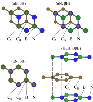
The stacking of graphene on hBN is a crucial point, however it was already shown that the configuration with the lowest energy is when one C atom is over the B atom and the other C atom is over the hollow site of hBN [82].
Before we proceed, we define a terminology to make sense of the structural arrangements, used in the following. We denote the three relevant sites in hBN as the B site (boron), the N site (nitrogen), and the H site (hollow position in the center of the hexagon). Similarly, we have two graphene sublatticesα(CA) andβ(CB). We call the energetically most favorable configuration (αB,βH), where CA is over boron, and CBis over the hollow site. According to this definition we define the other configurations as (αN,βH) and (αN,βB).
Due to symmetry, the configurations with interchanged CA and CBsublattices give the same results. The lowest energy interlayer distances between graphene and hBN are different for the different stackings [82]. We include a distance study for all three configurations, in order to reveal what are the corresponding lowest energy distances.
FIG. 1. Three high-symmetry commensurate stacking configu- rations of graphene on hBN, (αB,βH), (αN, βH), and (αN,βB) and the (HαH, BβB) geometry, as an example of hBN encapsulated graphene.
In analogy, a stacking sequence of hBN encapsulated graphene is then abbreviated as (UαV, XβY), indicating that theα(β) sublattice of graphene is sandwiched between the U and V (X and Y) sites of top and bottom hBN, each of which can take the values {B, N, H}. It has been shown [81] that the energetically most favorable sandwich structure is (HαH, BβB) in agreement with our findings here, meaning thatα(β) is sandwiched between the two H sites (B sites) of top and bottom hBN. Interlayer distances, used in the encapsulated geometries, are the ones determined by the distance study of the nonencapsulated structures. In Fig. 1we show the three commensurate stacking configurations of graphene on hBN, as well as the (HαH, BβB) geometry, as an example of hBN encapsulated graphene.
First-principles calculations are performed with full po- tential linearized augmented plane wave (FLAPW) code based on DFT [83] and implemented in WIEN2k [84].
Exchange-correlation effects are treated with the generalized- gradient approximation (GGA) [85], including dispersion correction [86] and using a k-point grid of 42×42×1 in the hexagonal Brillouin zone if not specified otherwise. The values of the muffin-tin radii we use arerC=1.34 for C atom, rB=1.27 for B atom, andrN=1.40 for N atom. We use the plane wave cutoff parameterRKMAX=9.5. In order to avoid interactions between periodic images of our slab geometry, we add a vacuum of at least 20 Å in thezdirection.
III. MODEL HAMILTONIAN & FULL BAND STRUCTURE The band structure of proximitized graphene can be modeled by symmetry-derived Hamiltonians [87]. For
−7
−6
−5
−4
−3
−2
−1 0 1 2 3 4 5
Γ M K Γ
E − EF[eV]
hBN graphene
ε1VB εVB2 ε1CB
εCB2
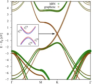
FIG. 2. Calculated electronic band structure of the (HαH, BβB) geometry, see Fig.1. The bands of graphene (hBN) are plotted in brown (green). The left inset shows a sketch of the low energy dispersion close to the K point. Due to the presence of the substrate, graphene’s low energy bands are split into four statesε1/2CB/VB, with a band gap.
(hBN)/graphene/hBN heterostructures havingC3vsymmetry, the effective low energy Hamiltonian is
H=H0+H+HI+HR+HPIA, (1) H0 =hv¯ F(τkxσx−kyσy)⊗s0, (2) H=σz⊗s0, (3) HI=τ
λAIσ++λBIσ−
⊗sz, (4) HR= −λR(τσx⊗sy+σy⊗sx), (5) HPIA=a
λAPIAσ+−λBPIAσ−
⊗(kxsy−kysx). (6) HerevF is the Fermi velocity and the in-plane wave vector componentskxandkyare measured from±K, corresponding to the valley indexτ = ±1. The Pauli spin matrices are si, acting on spin space (↑,↓), and σi are pseudospin matri- ces, acting on sublattice space (CA, CB), withi= {0,x,y,z}
andσ±=12(σz±σ0). The lattice constant isa=2.46 Å of pristine graphene and the staggered potential gap is. The parametersλAI andλBI describe the sublattice resolved intrinsic SOC, λR stands for the Rashba SOC, and λAPIA and λBPIA are the sublattice resolved pseudospin-inversion asymmetry (PIA) SOC parameters. The basis states are|A,↑,|A,↓,
|B,↑, and|B,↓, resulting in four eigenvaluesε1/2CB/VB. The calculated band structure of encapsulated graphene in the (HαH, BβB) configuration is shown in Fig. 2, as a representative example for all considered geometries. Other stacking geometries, as well as graphene on hBN, exhibit similar band features. The Dirac bands of graphene are located within the hBN band gap. In general, the geometries we consider in the following have broken pseudospin symmetry,
−80
−60
−40
−20 0 20 40 60 80
M ← K → Γ
1.5 1 0.5 0 0.5 1 1.5
E − EF[meV]
k [10−2/Å]
Model DFT
10 15 20 25
M ← K → Γ
splitting [μeV]
val cond
−1
−0.5 0 0.5 1
M ← K → Γ
< sx>
−1
−0.5 0 0.5 1
M ← K → Γ
< sy>
−1
−0.5 0 0.5 1
M ← K → Γ
< sz>
(a)
(b)
(c)
(d)
(e)
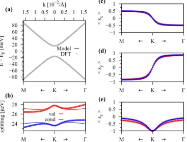
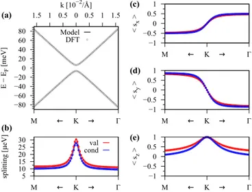
FIG. 3. Calculated band properties of graphene on hBN in the vicinity of the K point for (αB,βH) configuration and an interlayer distance of 3.35 Å. (a) First-principles band structure (symbols) with a fit to the model Hamiltonian (solid line). (b) The splitting of conduction bandECB(blue) and valence bandEVB(red) close to the K point and calculated model results. (c)–(e) The spin expectation values of the bandsεVB2 andεCB1 and comparison to the model results.
The fit parameters are given in TableI.
and a band gap opens in graphene. Then, e.g., CA orbitals form the conduction band (CB), while CB ones form the valence band (VB). Further, the low energy bands split into four statesεCB/VB1/2 due to SOC and the Rashba effect, see left inset in Fig.2. The general strategy is now to calculate the low energy bands and extract the model Hamiltonian parameters best fitting the DFT results, for all (hBN)/graphene/hBN geometries.
IV. GRAPHENE ON HBN
In this section we discuss the graphene/hBN heterostruc- tures. We show our fit results to the low energy Hamiltonian for the different stacking configurations and analyze the influ- ence of the interlayer distance, between graphene and hBN, on the extracted orbital and SOC model parameters. Furthermore, we show and discuss calculated spin-orbit fields. Before we turn to the calculation of the SR properties, we show the tun- ability of the parameters by applying a transverse electric field for one specific stacking configuration. Finally, we discuss the accuracy of the model, analyze atomic SOC contributions, and consider an arbitrary but special graphene/hBN stack.
A. Low energy bands
In Fig.3we show the calculated low energy band structure in the vicinity of the K point with a fit to our minimal tight-binding Hamiltonian for the (αB,βH) configuration of graphene on hBN. We can see that the orbital band struc- ture is perfectly reproduced by our model, see Fig. 3(a), in a quite large energy window around the Fermi level. The splittings of the bands are shown in Fig.3(b), which are in the μeV range and are defined as ECB=ε2CB−ε1CB and EVB=ε2VB−εVB1 . Also the splittings are nicely reproduced
−80
−60
−40
−20 0 20 40 60 80
M ← K → Γ
1.5 1 0.5 0 0.5 1 1.5
E − EF[meV]
k [10−2/Å]
Model DFT
24 26 28
M ← K → Γ
splitting [μeV]
val cond
−1
−0.5 0 0.5 1
M ← K → Γ
< sx>
−1
−0.5 0 0.5 1
M ← K → Γ
< sy>
−1
−0.5 0 0.5 1
M ← K → Γ
< sz>
(a)
(b)
(c)
(d)
(e)
FIG. 4. Calculated band properties of graphene on hBN in the vicinity of the K point for (αN,βH) configuration and an interlayer distance of 3.50 Å. (a) First-principles band structure (symbols) with a fit to the model Hamiltonian (solid line). (b) The splitting of conduction bandECB(blue) and valence bandEVB(red) close to the K point and calculated model results. (c)–(e) The spin expectation values of the bandsεVB2 andεCB1 and comparison to the model results.
The fit parameters are given in TableI.
by the model, with a maximum discrepancy of about 10%
compared to the first-principles data. More specifically, the splittings are overestimated (underestimated) along the K-M (K-) path, by the model. The reason for the discrepancy of the fit will be explained at a later point. Finally, Figs.3(c)–3(e) show the spin expectation values of the bandsε2VBandεCB1 , which are in perfect agreement with the model. The sx and sy spin expectation values show a pronounced signature of Rashba SOC, with a sign change around the K point. The sz expectation values are maximum at the K point, slowly decaying away from it.
In Figs.4and5we show the fits to the model Hamiltonian for the (αN,βH) and (αN,βB) configurations. The overall results look similar to the (αB,βH) configuration. The or- bital band structure, splittings, and spin expectation values are again nicely reproduced by the model. Compared to the (αB, βH) case, band splittings are even better reproduced in these two cases, with a maximum discrepancy of 3% and 1%, respectively. Thesxandsyspin expectation values again show the characteristic signature of Rashba SOC, originating from the broken inversion symmetry of graphene, due to the hBN substrate. However, thesz expectation values, also decaying away from K, are opposite compared to the (αB, βH) case. We find that our model is very robust and different stacking configurations are described by different parameter sets. The extracted parameters are given in TableIfor the three commensurate high-symmetry graphene/hBN stacking con- figurations, with their corresponding lowest energy distance.
B. Distance study
One has to mention that different stacking configurations lead to different interlayer distances between graphene and
−80
−60
−40
−20 0 20 40 60 80
M ← K → Γ
1.5 1 0.5 0 0.5 1 1.5
E − EF[meV]
k [10−2/Å]
Model DFT
24 28 32 36 40
M ← K → Γ
splitting [μeV]
val cond
−1
−0.5 0 0.5 1
M ← K → Γ
< sx>
−1
−0.5 0 0.5 1
M ← K → Γ
< sy>
−1
−0.5 0 0.5 1
M ← K → Γ
< sz>
(a)
(b)
(c)
(d)
(e)
FIG. 5. Calculated band properties of graphene on hBN in the vicinity of the K point for (αN,βB) configuration and an interlayer distance of 3.55 Å. (a) First-principles band structure (symbols) with a fit to the model Hamiltonian (solid line). (b) The splitting of conduction bandECB(blue) and valence bandEVB(red) close to the K point and calculated model results. (c)–(e) The spin expectation values of the bandsε2VBandε1CBand comparison to the model results.
The fit parameters are given in TableI.
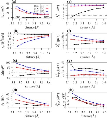
hBN, when minimizing the total energy of the individual geometries. In Fig.6we show the fit parameters, as a function of the distance between graphene and hBN, for the three stacking configurations. We find that the total energy is lowest for the (αB, βH) configuration with an interlayer distance of 3.35 Å, see Fig. 6(a). The lowest energies for the (αN, βH) and (αN, βB) configurations are obtained at distances of 3.50 Å and 3.55 Å. The Fermi velocityvF, see Fig.6(b), which reflects the nearest neighbor hopping strength viat=
2 ¯√hvF
3a, grows as a function of distance, especially for the (αN, βH) and (αN, βB) configurations. In contrast to that, the gap parameterdecreases with distance, in agreement with literature [82]. When moving the graphene away from the substrate, the sublattice symmetry breaking reduces and the gap decreases.
One very important observation is that the gap parameter of the (αB,βH) configuration is opposite in sign compared to the other configurations, as seen in a moiré pattern [88–90].
In the (αB,βH) configuration, the CA sublattice is over the boron. Sublattice CAforms, in this case, the VB which is why we need a negative value of in the model, to match the sublattice character of the DFT results. In contrast, the other configurations have the CAsublattice over the nitrogen, which then forms the CB, leading to a positive value of . This also explains why thesz spin expectation values for different configurations are different, compare Figs.3(e) and4(e). In a moiré pattern geometry, with micrometer size flakes of graphene and hBN, all of these local stacking configurations appear simultaneously. Consequently, there can be a local stacking geometry where the orbital gap closes, appearing when the two sublattices feel the same surrounding potential.
We will calculate and discuss such a situation at a later point, for a certain choice of stacking.
TABLE I. Fit parameters for the three graphene/hBN stacks at their energetically most favorable distances. The Fermi velocityvF, gap parameter, Rashba SOC parameterλR, intrinsic SOC parametersλAI andλBI, and PIA SOC parametersλAPIA andλBPIA. In the last row we average over the configurations for each parameter.
Configuration distance [Å] vF/105[ms] [meV] λR[μeV] λAI [μeV] λBI [μeV] λAPIA[μeV] λBPIA[μeV]
(αB,βH) 3.35 8.308 −17.08 10.65 5.00 9.37 33.58 37.57
(αN,βH) 3.50 8.197 16.31 12.67 11.78 13.96 4.431 26.68
(αN,βB) 3.55 8.128 23.50 17.89 12.21 15.82 12.91 29.73
average 3.47 8.211 7.577 13.74 9.66 13.05 16.97 31.33
The Rashba SOC parameter, see Fig.6(d), also decreases with distance. When the distance between graphene and hBN approaches infinity, the inversion symmetry of graphene is restored and the Rashba SOC parameter vanishes. The two intrinsic SOC parametersλAI andλBI approach the intrinsic SOC of 12μeV of pristine graphene [14], as we increase the distance, see Figs. 6(e) and 6(f). Finally, we find that the two PIA SOC parameters λAPIA and λBPIA, see Figs.6(g) and6(h), also decrease with distance. Overall, as expected, we restore the pristine graphene properties, as the interlayer distance gradually increases.
C. Spin-orbit fields
In Fig.7we show the calculated dispersion as a 2D map in kx-ky plane in the vicinity of the K point for the (αB,
0 20 40 60
3.1 3.2 3.3 3.4 3.5 3.6 Etot[meV]
distance [Å]
(αB, βH) (αN, βH) (αN, βB)
7.4 7.6 7.8 8 8.2 8.4
3.1 3.2 3.3 3.4 3.5 3.6 vF/105 [m/s]
distance [Å]
−50 0 50 100
3.1 3.2 3.3 3.4 3.5 3.6
∆[meV]
distance [Å]
0 20 40 60
3.1 3.2 3.3 3.4 3.5 3.6 λR[μeV]
distance [Å]
−4 0 4 8 12
3.1 3.2 3.3 3.4 3.5 3.6 λIA[μeV]
distance [Å]
0 105 1520 25 30
3.1 3.2 3.3 3.4 3.5 3.6 λIB[μeV]
distance [Å]
0 20 40 60
3.1 3.2 3.3 3.4 3.5 3.6 λPIAA[μeV]
distance [Å]
0 25 50 75 100 125
3.1 3.2 3.3 3.4 3.5 3.6 λPIAB[μeV]
distance [Å]
(a)
(b)
(c)
(d)
(e)
(f)
(g)
(h)
FIG. 6. Fit parameters as a function of interlayer distance be- tween graphene and hBN for the three different stacking configu- rations. (a) Total energy, (b) the Fermi velocityvF, (c) gap parameter , (d) Rashba SOC parameterλR, (e) intrinsic SOC parameterλAI for sublattice A, (f) intrinsic SOC parameterλBI for sublattice B, (g) PIA SOC parameterλAPIA for sublattice A, and (h) PIA SOC parameter λBPIAfor sublattice B.
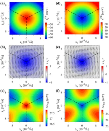
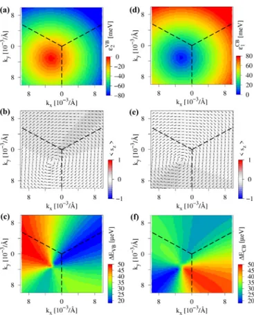
βH) configuration. The energies of the bands,ε2VBandεCB1 , do not show any trigonal warping, see Figs. 7(a) and7(d).
However, already the spin texture shows that trigonal warping is present with a very pronounced Rashba spin-orbit field, rotating in a clockwise direction, see Figs.7(b)and7(e), as expected from the inversion symmetry breaking by the hBN substrate. In contrast to the CB, the VB sz spin expectation value strongly decays away from the K point. A pronounced threefold symmetry is observed in the spin splittingsEVB and ECB, see Figs. 7(c) and 7(f). Along the K- path, the Dirac bands are more split than along the K-M path.
As we have seen, our model Hamiltonian agrees very well
FIG. 7. Calculated low energy dispersion of graphene on hBN around the K point for (αB, βH) configuration and an interlayer distance of 3.35 Å. (a) 2D map of the energy of the valence bandεVB2 , with the corresponding spin texture of the band shown in (b) and the splitting of the valence bandEVB=ε2VB−ε1VBshown in (c). (d)–(f) The same as (a)–(c) but for conduction bandεCB1 and conduction band splittingECB=ε2CB−εCB1 . The dashed lines show the edges of the Brillouin zone with the K point at the center.
FIG. 8. Calculated low energy dispersion of graphene on hBN around the K point for (αN, βH) configuration and an interlayer distance of 3.50 Å. (a) 2D map of the energy of the valence bandεVB2 , with the corresponding spin texture of the band shown in (b) and the splitting of the valence bandEVB=εVB2 −εVB1 shown in (c). (d)–(f) The same as (a)–(c) but for conduction bandε1CBand conduction band splittingECB=εCB2 −εCB1 . The dashed lines show the edges of the Brillouin zone with the K point at the center.
on a qualitative level for this case, see Fig. 3, however the band splittings cannot be fully recovered. The reason will be explained in the last subsection. In Figs. 8 and 9 we show the calculated dispersion as a 2D map in thekx-ky plane in the vicinity of the K point for the (αN, βH) and (αN,βB) configurations. The overall trigonal symmetry features remain and are very similar to the (αB,βH) configuration. Especially for the (αN,βB) configuration, only weak trigonal symmetry, around the K point, can be observed.
D. Transverse electric field
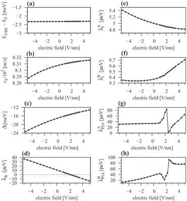
In experiment gating is required to tune the Fermi level towards the charge neutrality point. By using top and back gate electrodes, one can tune the doping level and simultane- ously apply an electric field across a heterostructure. Thereby the transverse electric field can influence electronic and spin- orbit properties of graphene, especially the Rashba SOC [14].
We consider the lowest energy configuration (αB, βH) for graphene on hBN and apply a transverse electric field, which is modeled by a zigzag potential, across the heterostructure.
For every magnitude of the field we calculate the low energy band structure and fit it to the model Hamiltonian. In Fig.10we show the fit parameters for (αB,βH) configuration as a function of external electric field. Indeed, we can tune
FIG. 9. Calculated low energy dispersion of graphene on hBN around the K point for (αN, βB) configuration and an interlayer distance of 3.55 Å. (a) 2D map of the energy of the valence bandεVB2 , with the corresponding spin texture of the band shown in (b) and the splitting of the valence bandEVB=ε2VB−εVB1 shown in (c). (d)–(f) The same as (a)–(c) but for conduction bandεCB1 and conduction band splittingECB=ε2CB−ε1CB. The dashed lines show the edges of the Brillouin zone with the K point at the center.
most of the parameters. The Fermi velocity vF, as well as intrinsic SOC parameters λAI and λBI, are barely affected.
However, the field can tune the orbital gap, Rashba and PIA SOC parameters. Especially the Rashba parameter can be tuned over a wide range, even from positive to negative values, with the transition at around 2 V/nm. Tuning the Rashba SOC parameter, from a positive to a negative value, also allows us to change the rotation direction of the spin-orbit fields, see Figs.7(b)and7(e). Most importantly we can tune the Rashba SOC from a finite value to zero. Consequently, we can control the strength of the in-plane spin-orbit field, dictated by Rashba SOC, which will significantly influence spin transport and SR properties. Another feature we notice is that around 2 V/nm, the PIA SOC parameters are not changing very smoothly with applied field, which is connected with the transition of the Rashba SOC through zero.
E. Spin relaxation anisotropy
Since the low energy HamiltonianHcan nicely reproduce the dispersion around the K point, we can use it together with our fit parameters to calculate SR times. We calculate, for a very dense kgrid in the vicinity of the K point, the energy spectrum and spin expectation values for the Dirac bands from
−3
−2.5
−2
−1.5
−4 −2 0 2 4
EVBE− EF[meV]
electric field [V/nm]
8.28 8.29 8.3 8.31 8.32
−4 −2 0 2 4
vF/105[m/s]
electric field [V/nm]
−24
−20
−16
−12
−4 −2 0 2 4
∆[meV]
electric field [V/nm]
−20
−10102030400
−4 −2 0 2 4
λR[μeV]
electric field [V/nm]
4.8 5 5.2 5.4
−4 −2 0 2 4
λIA[μeV]
electric field [V/nm]
9.3 9.4 9.5 9.6 9.7
−4 −2 0 2 4
λIB[μeV]
electric field [V/nm]
0 20 40 60 80
−4 −2 0 2 4
λPIAA[μeV]
electric field [V/nm]
20 40 60 80 100
−4 −2 0 2 4
λPIAB[μeV]
electric field [V/nm]
(a)
(b)
(c)
(d)
(e)
(f)
(g)
(h)
FIG. 10. Fit parameters as a function of the applied transverse electric field for the (αB,βH) configuration. (a) Valence band edge with respect to the Fermi level, (b) the Fermi velocityvF, (c) gap parameter , (d) Rashba SOC parameter λR, (e) intrinsic SOC parameterλAI for sublattice A, (f) intrinsic SOC parameterλBI for sublattice B, (g) PIA SOC parameterλAPIAfor sublattice A, and (h) PIA SOC parameterλBPIAfor sublattice B.
our model. To calculate the SR time, we define the spin-orbit field componentsωk,ias [62]
ωk,i=Ek
¯ h · sk,i
sk
, (7)
where k is the momentum and sk,i are the spin expectation values along the direction i= {x, y, z}. The energy splitting of the Dirac bands is Ek and sk=√
s2k,x+s2k,y+s2k,z is the absolute value of the spin. By that we obtain at eachk point the spin-orbit vector field. Following the derivation of Refs. [71,91], we then calculate the SR times as follows
τs−1,x(E)=τp· ω2k,y
+τiv· ω2k,z
, (8)
τs−,y1(E)=τp· ω2k,x
+τiv· ω2k,z
, (9)
τs−,z1(E)=τp·
ω2k,x+ωk2,y
. (10)
The average·is taken over allk points that have the same constant energyE. The momentum relaxation time isτp and τiv is the intervalley scattering time. For the calculation of the averages · we use energy steps of 100μeV with a smearing of ±50μeV, corresponding to a temperature of 0.58 K. Measurements [37–40] provide SR lengths of λs≈ 20μm, SR times ofτs≈8 ns, and spin diffusion constants of Ds≈0.04 ms2. With the relation λs=√
τsDs and using that the spin diffusion constant is roughly equal to the charge diffusion constantDs≈Dc= 12vF2τpandvF≈8×10⁵ ms, we
0 5 10 15 20
−100 −80 −60 −40 −20 0 20 40 60 80 100
time [ns]
E − EF[meV]
τs,x τs,y τs,z (a)
(b)
FIG. 11. Calculated SR times and anisotropies for (αB, βH) configuration. (a) Color map of the SR anisotropyξ=τs,z/τs,x as a function ofN=τiv/τpand the energy. (b) Individual SR times as a function of energy corresponding to the dashed line in (a) with τp=125 fs andτiv =8·τp. The gray lines indicate the band edges.
getτp=125 fs, which we use in the calculations. The value forτpis reasonable, assuming ultraclean samples.
Since intervalley scattering times are hard to estimate from experiments, we consider it variable, τiv=N·τp withN= {1, ...,15}, for our calculations. By that we obtain the SR time as a function of the energy, for spins along thex,y, and z direction for each ratioN =τiv/τp. More interesting than the individual SR times is the SR anisotropyξ =τs,z/τs,x, a measurable fingerprint of the SOC of the system.
We show a color map of the calculated anisotropyξ as a function ofN and the energy for the (αB,βH) configuration in Fig. 11(a). Within the band gap of ±17 meV, of course no states are available and SR times cannot be calculated, because the smearing we use is only 0.58 K. For holes we find that the anisotropy isξ ≈12, the Rashba limit, as soon as we are below−20 meV from the valence band edge, for each ratioN. For electrons the situation is completely different and the anisotropy can get very large, even 20 meV away from the conduction band edge. We also find that, independent of N, the anisotropy is largest close to the band edges, which would correspond to the charge neutrality point in experiment.
In Fig.11(b)we show the individual SR times as a function of energy, corresponding toN=8. We find SR times of around 10 ns, consistent with measurements [40]. However, we have to keep in mind that Fig.11is only valid for a certain stacking configuration, the (αB,βH) one, of graphene on hBN.
In experiment one expects that electrons traveling through graphene on a hBN substrate would rather experience local
0 5 10 15
−100 −80 −60 −40 −20 0 20 40 60 80 100
time [ns]
E − EF[meV]
τs,x τs,y τs,z (a)
(b)
FIG. 12. Calculated SR times and anisotropies for graphene on hBN. Here we use the averaged parameters of the graphene/hBN heterostructures given in the main text. (a) Color map of the SR anisotropyξ=τs,z/τs,xas a function ofN=τiv/τp and the energy.
(b) Individual SR times as a function of energy corresponding to the dashed line in (a) withτp=125 fs andτiv=8·τp. The gray lines indicate the band edges.
spin-orbit fields that can be very different for certain regions due to the different stacking configurations. Therefore, in Fig.12(a)we show a color map of the calculated anisotropyξ as a function ofNand the energy when using the averaged pa- rameters of graphene on hBN given in TableI. This averaged situation should correspond to a more realistic situation in a real heterostructure, where all kinds of stacking configurations are present simultaneously. We find that electrons have an anisotropy ratioξ ≈ 12 almost independent ofN and the en- ergy, see Fig.12(b), clearly different from the pure (αB,βH) configuration, compare to Fig.11. Close to the band edges, i.e., the charge neutrality point, the anisotropy can reach very large values. For holes the anisotropy varies aroundξ ≈1 for moderate doping densities.
So far, anisotropies of ξ ≈1 have been measured for graphene on hBN and SiO2 [26,27,38,92,93], in agreement with our averaged parameter results. A first indication of large anisotropies was found in hBN encapsulated bilayer graphene heterostructures [69,70]. There it was shown that the anisotropyξ decreases with increasing carrier density, in line with our results for monolayer graphene. They also showed that the anisotropy, at fixed doping level, can be strongly enhanced by an applied electric field.
In dual gated structures, one can individually tune the doping level and the electric field across the heterostructure.
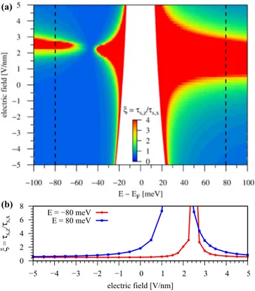
In Fig. 13 we show the SR anisotropy ξ, specifically for
0 2 4 6 8
−5 −4 −3 −2 −1 0 1 2 3 4 5
ξ= τs,z/τs,x
electric field [V/nm]
E = −80 meV E = 80 meV (a)
(b)
FIG. 13. (a) Calculated SR anisotropyξ=τs,z/τs,xas a function of energy and applied transverse electric field for (αB, βH) con- figuration, using τp=125 fs and τiv=8·τp. (b) Anisotropy ξ at energiesE = ±80 meV corresponding to the dashed lines in (a).
(αB,βH) configuration as a function of energy and applied transverse electric field, using the parameter sets for several finite electric field strengths, see Fig. 10. We find that the anisotropy is strongly tunable by means of external gating.
At around 2 V/nm we find a very strong enhancement of the anisotropy, which is related to the zero transition of the Rashba SOC parameter. The anisotropy is giant forλR≈0, as the states are then mainlyszpolarized. In Fig.13(b)we show that an electric field can tune the anisotropy by one order of magnitude at a fixed doping level.
F. Additional considerations
We now want to clarify two remaining issues: (i) Where does the discrepancy between the model and the first- principles data, see Fig. 3(b), come from? (ii) Is there a low-symmetry stacking configuration, where the orbital gap closes?
1. Model discrepancy
In the case of the (αB,βH) configuration, we have found that the splittings are overestimated (underestimated) along the K-M (K-) path, by the model. The discrepancy in the splitting of the bands is due to the influence of the substrate.
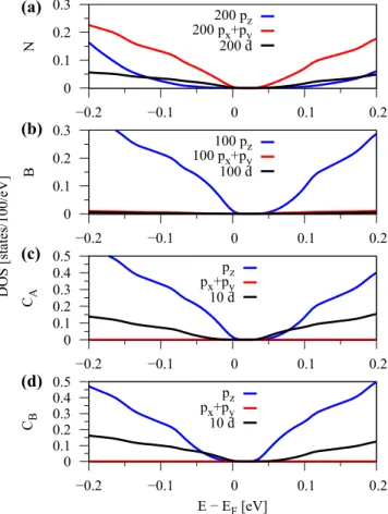
In general, the model HamiltonianHjust considers effective π orbitals of graphene, however there seems to be a subtle influence from a hybridization to the p orbitals of hBN. If we look at the density of states (DOS) for the (αB, βH) case, see Fig.14, we find that close to the Dirac point there
0 0.1 0.2 0.3
−0.2 −0.1 0 0.1 0.2
DOS [states/100/eV] N
200 pz 200 px+py 200 d
0 0.1 0.2 0.3
−0.2 −0.1 0 0.1 0.2
B
100 pz 100 px+py 100 d
0 0.1 0.2 0.3 0.4 0.5
−0.2 −0.1 0 0.1 0.2
CA
pz px+py 10 d
0 0.1 0.2 0.3 0.4 0.5
−0.2 −0.1 0 0.1 0.2
CB
E − EF[eV]
pz px+py 10 d
(a)
(b)
(c)
(d)
FIG. 14. Density of states of graphene on hBN around the Fermi level for (αB,βH) configuration and an interlayer distance of 3.35 Å.
The DOS is multiplied by a factor of 100. Each subfigure (a)–(d) cor- responds to a different atom. For each atom, the orbital contributions to the DOS are multiplied with the corresponding prefactor. The DOS is calculated with ak-point grid of 180×180×1.
is a small contribution from nitrogen and boron p states.
Especially boronpzorbitals and nitrogenpx+pyorbitals are contributing close to the charge neutrality point. Moreover, from our distance study we find that the discrepancy between the model and the first-principles data is getting smaller as we increase the interlayer distance.
Finally, we calculate the low energy band structures, when SOC is artificially turned off on the nitrogen, boron, or carbon atoms, respectively. The fit parameters for these situations are given in TableII, along with the maximum discrepancy for
each situation. When SOC of the boron atom is turned off, the parameters and the fit accuracy are barely different. A severe improvement of the fit is accomplished, when SOC of the nitrogen atom is turned off, reflected in the strongly reduced discrepancy between model and DFT data. Furthermore, if we turn off SOC on the carbon atoms of graphene, we can identify the contribution solely coming from the substrate, where we find negative intrinsic SOC parametersλAI andλBI. Thus, nitrogen gives a non-negligible contribution to the SOC splitting of the Dirac bands.
From our analysis, we conclude that the discrepancy comes from nitrogen px+pyorbitals that hybridize withπ orbitals of graphene. Already such a very small contribution of px+ pyorbitals, see Fig.14(a), can substantially influence the spin splitting and an effective model, based only on π orbitals of graphene, can no longer perfectly describe the results.
However, the overall fit is still very good and sufficient for our needs.
2. Gap closing stacking
We have seen that different stackings can lead to a different sign of the gap parameter, see Table I. Consequently, as already mentioned, a local stacking geometry can exist, in a real moiré pattern geometry, that has a closed orbital gap. In Fig.15we show the low energy band properties of an arbitrary stacking geometry, without having any symmetry [94].
First of all, we notice that the Dirac point is no longer located at the K point. From the corresponding geometry in Fig. 15(a), we find that the hoppings, from say CA to the three nearest neighbors CB, are all different due to the substrate. This asymmetry in the nearest neighbor hopping amplitudes leads to the shift of the Dirac point in momentum space [95,96]. Since our model Hamiltonian considers only high-symmetry stacking configurations, without shifted Dirac cone, we cannot fit the data with it. From the spin expectation values we find a very pronounced Rashba spin-orbit field, as theszcomponent is strongly suppressed.
In order to identify the location of the Dirac point in momentum space, we calculate the dispersion as a 2D map in kx-ky plane in the vicinity of the K point, see Fig. 16.
Indeed, we find that the Dirac point is shifted away from the corner of the Brillouin zone. At the Dirac point, the orbital gap is 1.64 meV large. Due to the limited number ofkpoints in the calculation grid for the 2D map, we cannot identify the exact position of the Dirac point, so the orbital gap is not fully closed but much smaller than in the high-symmetry TABLE II. Summary of the fitting parameters of HamiltonianH, for graphene on hBN for (αB,βH) configuration and an interlayer distance of 3.35 Å. Here, we have artificially turned off SOC on nitrogen, boron, or carbon atoms, respectively. The Fermi velocityvF, gap parameter, Rashba SOC parameterλR, intrinsic SOC parametersλAI andλBI for sublattice A and B, and PIA SOC parametersλAPIAandλBPIA
for sublattice A and B. The discrepancy is the calculated residual of the fit along the M-K-path given in arbitrary units.
SOC on vF/105[ms] [meV] λR[μeV] λAI [μeV] λBI [μeV] λAPIA[μeV] λBPIA[μeV] discr. [a.u.]
N, B, C 8.308 −17.08 10.65 5.00 9.37 33.58 37.57 1.265
N, C 8.308 −17.08 12.22 5.01 8.95 34.65 34.82 1.269
B, C 8.308 −17.08 10.23 12.08 12.66 −0.06 −34.82 0.260
N, B 8.308 −17.07 −1.82 −7.09 −2.79 −9.53 66.55 1.349
C 8.308 −17.07 11.85 12.07 12.25 −4.60 −32.67 0.268
−80
−60
−40
−20 0 20 40 60 80
M ← K → Γ
1 0.5 0 0.5 1 1.5
E − EF[meV]
k [10−2/Å]
DFT
20 30 40 50
M ← K → Γ
splitting [μeV] val
cond
−1
−0.5 0 0.5 1
M ← K → Γ
< sx>
−1
−0.5 0 0.5 1
M ← K → Γ
< sy>
−1
−0.5 0 0.5 1
M ← K → Γ
< sz>
(a)
(b)
(c)
(d)
(e)
FIG. 15. Calculated band properties of graphene on hBN in the vicinity of the K point and an interlayer distance of 3.45 Å. (a) First- principles band structure and local stacking geometry. (b) The split- ting of conduction bandECB(blue) and valence bandEVB(red) close to the K point. (c)–(e) The spin expectation values of the bands εVB2 andεCB1 .
stacking cases, see TableI. We also notice that the spin-orbit field is almost purely in-plane without anyszcomponent, see Figs. 16(b)and16(e), in a very large area around the Dirac point. Consequently, Rashba SOC plays an important role in this low-symmetry stacking configuration. If we look at the spin-orbit splitting of the bands, Figs. 16(c) and 16(f), we find that there is no trigonal symmetry remaining. Such a stacking configuration completely breaks the symmetry of the graphene, due to the different hopping amplitudes between nearest neighbors caused by the hBN substrate. Of course, in a moiré geometry, several other stackings are present that lead to very different local orbital gaps, spin-orbit fields, and spin splittings.
V. HBN ENCAPSULATED GRAPHENE
In this section we discuss the hBN/graphene/hBN het- erostructures. We show our fit results to the low energy Hamil- tonian for the different stacking configurations. Compared to the previous section, symmetry plays an important role when fitting the Hamiltonian. Again, we show the tunabil- ity of the parameters by applying a transverse electric field across the heterostructures. Finally we calculate SR times and anisotropies, and highlight differences to experimental findings in bilayer graphene.
A. Low energy bands
From our previous study of graphene on hBN, we already know what is the energetically most favorable distance for each stacking geometry, which we keep for the encapsulated cases, respectively. Depending on the stacking of the top and bottom hBN with respect to the graphene, different interlayer distances can be present. The stacking sequences are defined in analogy to the graphene on hBN cases. The energetically
FIG. 16. Calculated low energy dispersion of graphene on hBN around the K point for stacking configuration in Fig. 15 and an interlayer distance of 3.45 Å. (a) 2D map of the energy of the valence bandε2VB, with the corresponding spin texture of the band shown in (b) and the splitting of the valence bandEVB=ε2VB−εVB1 shown in (c). (d)–(f) The same as (a)–(c) but for conduction bandε1CBand conduction band splittingECB=εCB2 −εCB1 . The dashed lines show the edges of the Brillouin zone with the K point at the center.
most favorable configuration is (HαH, BβB), which we name C1 configuration. According to this, we define several other configurations.
For such a configuration, like (HαH, BβB)=C1, we re- cover the mirror symmetry of graphene, see Fig.1, reflected in theD3hsymmetric version of the Hamiltonian with vanishing Rashba and PIA contributions [87]. In Fig.17, we show the low energy band properties of the C1 configuration, along with a fit to our model Hamiltonian. We can see perfect agreement with the first-principles data, just using the four pa- rametersvF,,λAI , andλBI. Rashba and PIA SOC parameters are not necessary and strictly zero for the fit, especially for this mirror symmetric configuration, as explained. Therefore the bands are purelyszpolarized.
In Figs.18and19, we show the low energy band properties of the (BαN, NβH) and (NαN, BβH) configurations, along with a fit to our model Hamiltonian, as further examples of the robustness of the Hamiltonian. We can see again perfect agreement with the first-principles data. Even though the low energy band properties are somewhat similar, each configura- tion has a very individual parameter set.
The parameters, best fitting the DFT results, are given in TableIII. We find that there is another configuration, (HαB,