Single and bilayer graphene on the topological insulator Bi
2Se
3: Electronic and spin-orbit properties from first principles
Klaus Zollner
*and Jaroslav Fabian
Institute for Theoretical Physics, University of Regensburg, 93040 Regensburg, Germany
(Received 8 July 2019; revised manuscript received 14 October 2019; published 28 October 2019) We present a detailed study of the electronic and spin-orbit properties of single and bilayer graphene in proximity to the topological insulator Bi
2Se
3. Our approach is based on first-principles calculations, combined with symmetry derived model Hamiltonians that capture the low-energy band properties. We consider single and bilayer graphene on 1–3 quintuple layers of Bi
2Se
3and extract orbital and proximity induced spin-orbit coupling (SOC) parameters. We find that graphene gets significantly hole doped (350 meV), but the linear dispersion is preserved. The proximity induced SOC parameters are about 1 meV in magnitude, and are of valley-Zeeman type. The induced SOC depends weakly on the number of quintuple layers of Bi
2Se
3. We also study the effect of a transverse electric field that is applied across heterostructures of single and bilayer graphene above 1 quintuple layer of Bi
2Se
3. Our results show that band offsets, as well as proximity induced SOC parameters, can be tuned by the field. Most interesting is the case of bilayer graphene, in which the band gap, originating from the intrinsic dipole of the heterostructure, can be closed and reopened again, with inverted band character. The switching of the strong proximity SOC from the conduction to the valence band realizes a spin-orbit valve. Additionally, we find a giant increase of the proximity induced SOC of about 200% when we decrease the interlayer distance between graphene and Bi
2Se
3by only 10%. Finally, for a different substrate material Bi
2Te
2Se, band offsets are significantly different, with the graphene Dirac point located at the Fermi level, while the induced SOC strength stays similar in magnitude compared to the Bi
2Se
3substrate.
DOI: 10.1103/PhysRevB.100.165141 I. INTRODUCTION
van der Waals (vdW) heterostructures [1–3] and emerging proximity effects [4] are an ideal platform to induce tailored properties in two-dimensional (2D) materials. Prominent 2D material examples are semimetallic single layer graphene (SLG) [5], semiconducting transition-metal dichalcogenides (TMDCs) [6], and insulating hexagonal boron-nitride (hBN) [7]. Recently, also superconductors (NbSe
2) [8], and ferro- and antiferromagnets (CrI
3, Cr
2Ge
2Te
6, MnPSe
3) [9–14] have been added to the list of 2D materials. Within this ever- expanding field of vdW structures, there already are subfields, such as valleytronics [15–18], straintronics [19–21], twistron- ics [22,23], and spintronics [24–26], wherein several major achievements have been made, for example optical spin in- jection [27] in SLG or tunable valley polarization in a TMDC [28], which are only possible due to vdW heterostructures and proximity effects.
Another important large class of materials are the three- dimensional (3D) topological insulators such as [29] Bi
2Se
3, Bi
2Te
3, and Sb
2Te
3, which are also layered crystals, consist- ing of quintuple layers (QLs) of alternating chalcogen (Se, Te) and pnictogen (Bi, Sb) atoms, which are held together by vdW forces. However, the characteristic Dirac states with spin- momentum locking [30] emerge only when the top and bottom surfaces of the topological insulator decouple, occurring at already 5–6 QLs, as demonstrated by angle resolved pho- toemission spectroscopy [31] and first-principles calculations
*
klaus.zollner@physik.uni-regensburg.de
[32–34]. Since each QL is about 1 nm in thickness, these materials are in between the 2D and 3D regime, depending on how many QLs one investigates. Nevertheless, they are impor- tant for practical applications [35], due to their topologically protected [36,37] and well conducting surface states [38], and for proximity induced phenomena [39–42], since strong SOC is present. When the topological insulators act as a substrate, the 2D regime (1–2 QLs) is sufficient, as proximity effects are of short range nature.
Recently, the interface engineering of 2D materials has become an important topic [43,44]. Experimentalists and theorists are searching for material combinations with novel properties. Graphene, due to its extremely high electron mo- bility [45] and intrinsically small SOC [46], is perfectly suited for spintronics. In addition, this monolayer carbon sheet can be efficiently manipulated by short range proximity effects.
One can induce strong SOC, as well as magnetism in SLG
[39–41,47–49]. Similar to a TMDC [47,48], a topological
insulator strongly enhances the rather weak intrinsic SOC of
SLG from 10 μeV [46], to about 1–2 meV [39,41]. Phase co-
herent transport measurements of SLG on Bi
1.5Sb
0.5Te
1.7Se
1.3have shown Dyakonov-Perel type spin relaxation with prox-
imity induced SOC of at least 2.5 meV [41]. First-principles
calculations of SLG on Bi
2Se
3have found either pure intrinsic
or valley-Zeeman type SOC in the meV range, depending on
the twist angle [39]. As a consequence of the large induced
SOC in SLG, the spin lifetimes of electrons significantly
decrease [39,50], from nanoseconds down to the picosecond
range. Giant spin lifetime anisotropies, the ratio of out-of-
plane to in-plane spin lifetimes, can be achieved [39,50].
Bilayer graphene (BLG) is even more interesting, since only the layer closest to the proximitizing material gets mod- ified, allowing for highly efficient tuning of the proximity properties by gating and doping. Recent studies have shown short range proximity induced exchange or SOC in BLG on Cr
2Ge
2Te
6or WSe
2[51–53]. Due to the unique and tunable low energy band structure of BLG, all-electrical control of spin relaxation and polarization can be achieved in such heterostructures. The proposed spin-orbit and exchange valve effects [51,52] in proximitized BLG can lead to new oppor- tunities for spintronics devices. So far, there are only few experimental studies [54–57] of BLG on Bi
2Se
3. However, there is no detailed experimental and theoretical study of the electronic and spin-orbit properties of BLG interfaced with topological insulators.
The open questions we would like to address are as follows.
In the case of SLG on Bi
2Se
3, when valley-Zeeman SOC is predicted to be present [39] for 1 QL, how does the presence of more QLs influence this interesting result? (The result is interesting, since in the topological substrate the spin-orbit fields are in-plane, while the induced valley-Zeeman fields in graphene are out-of-plane.) Another important question is, what is the influence of the topological insulator on BLG?
What are the band offsets, doping levels, and orbital and spin-orbit proximity effects? How does the interlayer distance between SLG and Bi
2Se
3affect the magnitude of proximity SOC? Also, can an electric field tune SOC in SLG and BLG in proximity to the topological insulator? Strong hole doping of the SLG on Bi
2Se
3is predicted [39]. Can one find a different topological insulator with a better band alignment, such that the graphene Dirac point is near E
F?
In this article we investigate these questions using first- principles calculations of SLG and BLG on the topological insulator Bi
2Se
3. We study the proximity induced SOC in SLG and BLG, originating from the topological insulator, by varying the number of QLs of Bi
2Se
3from 1–3. Symmetry- derived low energy tight-binding model Hamiltonians for SLG and BLG are fitted to the first-principles band structures, to extract orbital and spin-orbit parameters of the proximitized materials. Our results show that the dispersion of SLG (BLG) is preserved, but strong hole doping appears, as the Dirac point is about 350 meV (200 meV) above the Fermi level.
The proximity induced SOC is about 1 meV in magnitude, but with opposite sign for A and B sublattice, the so called valley-Zeeman type. We find that the intrinsic SOC parame- ters increase by about 10% for every QL of Bi
2Se
3that we add, up to 3QLs. As proximity effects are short ranged, we expect this increase to saturate.
Furthermore, we study the effect of a transverse electric field on the low energy band parameters for 1 QL of Bi
2Se
3proximitizing SLG and BLG. The electric field can tune the SOC parameters, which can have significant impact for tuning spin lifetimes in SLG and BLG. In addition, the surface states of the topological insulator, as well as the Dirac points of SLG and BLG, can be tuned with respect to the Fermi level, by the field. Most interesting is the BLG case, in which only the low energy conduction band is strongly spin-orbit split for zero field, as a consequence of short range proximity effects, and atom and layer localized energy states. The tuning of the orbital gap of BLG, by gradually increasing the field, leads to
a gap closing and subsequent reopening, now with a strongly spin-orbit split valence band. Consequently, a spin-orbit valve effect can be realized, similar to BLG on a TMDC [52].
An interlayer distance study, between SLG and the Bi
2Se
3substrate, shows a giant increase of the proximity induced SOC of about 200%, when we decrease the interlayer distance by only 10%. Furthermore, an atomically modified substrate Bi
2Te
2Se, leads to a significantly different band alignment and enhanced proximity SOC in SLG. The Dirac point of SLG, as well as the surface states of the topological insulator, are now located at the Fermi level. Especially this system holds promise, for the simultaneous study of two very differ- ent spin-orbit fields: in-plane spin-momentum locking from the topological insulator and out-of-plane proximity induced spin-orbit field from SLG.
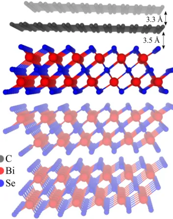
II. GEOMETRY AND COMPUTATIONAL DETAILS For the calculation of SLG and BLG on the topological insulator Bi
2Se
3, we consider 5 × 5 supercells of SLG and BLG (in Bernal stacking) on top of 3 × 3 supercells of Bi
2Se
3. Initial atomic structures are set up with the atomic simulation environment (ASE) [58]. We marginally stretch the lattice constant of graphene [5] to a = 2.486 Å and leave the Bi
2Se
3lattice constants [59] unchanged with a = 4.143 Å and c = 28 . 636 Å, using the atomic parameters (u , v) = (0.4008, 0.2117). We consider only geometries without relax- ation, using interlayer distances of 3.5 Å between the lowest graphene layer and the topmost QL of Bi
2Se
3, in agreement with recent studies [39], and an interlayer distance of 3.3 Å for the BLG, in agreement with experiment [60]. In Fig. 1 we show the geometry of SLG or BLG on top of 1–3 QLs of Bi
2Se
3, visualized with VESTA [61]. Compared to Ref. [39], we only study what they call the “large unit cell,” where no twist angle between the materials is present.
The electronic structure calculations are performed by den- sity functional theory (DFT) [62] with Quantum ESPRESSO [63]. Self-consistent calculations are performed with the k- point sampling of 9 × 9 × 1. Only for the largest heterostruc- tures, when 3QLs of Bi
2Se
3are considered, a smaller k- point sampling of 6 × 6 × 1 is used, due to computational limitations. We use an energy cutoff for charge density of 500 Ry, and the kinetic energy cutoff for wave functions is 60 Ry for the relativistic pseudopotentials with the projec- tor augmented wave method [64] with the Perdew-Burke- Ernzerhof exchange correlation functional [65]. We also add vdW corrections [66,67], and Dipole corrections [68] are included to get correct band offsets and internal electric fields.
In order to simulate quasi-2D systems, we add a vacuum of at least 24 Å to avoid interactions between periodic images in our slab geometry.
In contrast to the GW method, the generalized-gradient
approximation (GGA) used here is certainly not the most
accurate available choice to describe 3D topological insu-
lators [69–71]. Consequently, the charge transfer between
SLG (BLG) and the topological insulator, as well as dop-
ing and proximity SOC, can be different in more sophisti-
cated calculations. Still, the GGA does show the important
band structure features and it allows us to make predic-
tions for proximity effects in SLG/Bi
2Se
3heterostructures.
C Bi Se
3.3 Å 3.5 Å
FIG. 1. Geometry of SLG or BLG above 1–3 QLs of Bi
2Se
3. We highlighted the SLG / 1 QL structure, which is the minimal geometry we consider. Different colors correspond to different atomic species.
Furthermore, the systems we consider are too large, mak- ing GW calculations computationally inaccessible. In our GGA-based study, we believe that proximity effects can be captured quite nicely on a qualitative and semiquantitative level. For example, calculations [39] also using GGA have been used to analyze and interpret recent experiments of graphene/topological insulator structures [41].
III. MODEL HAMILTONIAN
It has been shown that a topological insulator induces strong proximity SOC in SLG [39,41], on the order of 1 meV.
Depending on the exact geometry (twist angle), either pure intrinsic or valley-Zeeman type SOC can be realized [39]. The valley-Zeeman SOC has also been observed in SLG/TMDC
heterostructures [47,48]. For BLG on a TMDC, even a spin- valve effect is proposed to be present [52]. We want to analyze in detail the influence of the topological insulator Bi
2Se
3on the low energy bands of SLG and BLG, in the previously mentioned (nontwisted) supercell configuration, where valley-Zeeman SOC has been found.
A. Graphene
The band structure of proximitized SLG can be modeled by symmetry-derived Hamiltonians [47–49,72–75]. For our heterostructures, the effective low energy Hamiltonian is
H
SLG= H
0+ H
+ H
I+ H
R+ H
PIA+ E
D, (1) H
0= hv ¯
F( τ k
xσ
x− k
yσ
y) ⊗ s
0, (2) H
= σ
z⊗ s
0, (3)
H
I= τ
λ
AIσ
++ λ
BIσ
−⊗ s
z, (4) H
R= −λ
R(τσ
x⊗ s
y+ σ
y⊗ s
x), (5) H
PIA= a
λ
APIAσ
+− λ
BPIAσ
−⊗ (k
xs
y− k
ys
x) . (6) Here v
Fis the Fermi velocity and the in-plane wave vector components k
xand k
yare measured from ±K, corresponding to the valley index τ = ±1. The Pauli spin matrices are s
i, acting on spin space (↑, ↓), and σ
iare pseudospin matrices, acting on sublattice space (C
A, C
B), with i = { 0 , x , y , z } . For shorter notation, we introduce σ
±=
12(σ
z± σ
0). The lattice constant of pristine graphene is a and the staggered potential gap is . The parameters λ
AIand λ
BIdescribe the sublat- tice resolved intrinsic SOC, λ
Rstands for the Rashba SOC, and λ
APIAand λ
BPIAare the sublattice resolved pseudospin- inversion asymmetry (PIA) SOC parameters. The basis states are |
A, ↑, |
A, ↓, |
B, ↑, and |
B, ↓, resulting in four eigenvalues ε
1CB/VB/2. Note that the model Hamiltonian de- scribes the dispersion relative to the graphene Dirac point. For the first-principles results doping can occur, shifting the Fermi level off the Dirac point. Therefore we introduce another parameter E
D, which generates a shift of the global model band structure. We call it the Dirac point energy.
B. Bilayer graphene
We wish to describe the low energy band structure of the proximitized BLG in the vicinity of the K and K
valleys.
Therefore, we introduce the following Hamiltonian derived from symmetry [76], where we keep only the most relevant terms:
H
BLG= H
orb+ H
soc+ E
D, (7)
H
orb=
⎛
⎜ ⎜
⎜ ⎜
⎝
+ V γ
0f (k ) γ
4f
∗(k) γ
1γ
0f
∗(k) V γ
3f (k) γ
4f
∗(k ) γ
4f (k) γ
3f
∗(k ) −V γ
0f (k )
γ
1γ
4f (k ) γ
0f
∗(k) − V
⎞
⎟ ⎟
⎟ ⎟
⎠ ⊗ s
0, (8)
H
soc=
⎛
⎜ ⎜
⎜ ⎝
τλ
A1Is
zi(λ
0+ 2λ
R)s
τ−0 0
−i(λ
0+ 2λ
R)s
τ+−τλ
B1Is
z0 0 0 0 τλ
A2Is
z− i( λ
0− 2 λ
R)s
τ−0 0 i(λ
0− 2λ
R)s
τ+−τλ
B2Is
z⎞
⎟ ⎟
⎟ ⎠ . (9)
1 0.5 0 0.5 1
M K M
E EF[eV] 0.5
0 0.5
< sz>
1 0.5 0 0.5 1
M K M
E EF[eV]
1 0.5 0 0.5 1
M K M
E EF[eV]
(a) (b) (c)
ED
ETI
FIG. 2. Calculated band structures of SLG on (a) one, (b) two, and (c) three QLs of Bi
2Se
3. The color is the s
zexpectation value. In (a) we define the Dirac point energy E
Dand the doping energy of the topological insulator E
TI.
We use the linearized version for the nearest-neighbor struc- tural function f (k ) = −
√23a(k
x− ik
y), with the graphene lat- tice constant a and the Cartesian components of the wave vector k
xand k
ymeasured from ±K for the valley index τ =
±1. Parameters γ describe intra- and interlayer hoppings of the BLG, when the lower (upper) graphene layer is placed in potential V (−V ). The parameter describes the asymmetry in the energy shift of the bonding and antibonding states. The parameters λ
Idescribe the intrinsic SOC of the corresponding layer and sublattice. The combination of parameters λ
0and λ
Rdescribe the global and local breaking of space inversion sym- metry. For a more detailed description of the parameters, we refer the reader to Ref. [76]. The basis is |
A1, ↑, |
A1, ↓,
|
B1, ↑ , |
B1, ↓ , |
A2, ↑ , |
A2, ↓ , |
B2, ↑ , and |
B2, ↓ . Similar to the SLG case, doping can occur, and again we denote the energy shift by the Dirac point energy E
D.
IV. BAND STRUCTURE, FIT RESULTS, AND SPIN-ORBIT FIELDS
Here we analyze the dependence of the proximity SOC in SLG and BLG on the number of QLs. We show the full calculated band structures, as well as a zoom to the low energy bands originating from SLG or BLG, being proximitized by the topological insulator, and fit the individual model Hamiltonians. The orbital and spin-orbit fit parameters are summarized in a tabular form.
A. Graphene
In Fig. 2 we show the full band structures of SLG above one, two, and three QLs of Bi
2Se
3. At the K point, one can recognize the Dirac bands originating from bare SLG [46], while at the point, the surface states of the topological insulator form. By gradually increasing the number of QLs, the Dirac bands of Bi
2Se
3start to form. We do not show a zoom to the surface bands of Bi
2Se
3, as we are mainly interested in proximity induced SOC in SLG and BLG. How- ever, one would see a pair of linear bands at the point,
each originating from one surface of the topological insulator, which still hybridize for 3 QLs only, exhibiting a gap. At first glance the bands of SLG seem to be not affected by adding more QLs. We find that SLG gets hole doped, as the Dirac point is shifted roughly 350 meV above the Fermi level. Only for 3 QLs, the Dirac point is at about 500 meV, which happens to appear due to the thicker topological insulator, consistent with recent calculations [39].
−0.5 0 0.5
M ← K → Γ
2 1 0 1 2
VB1
k [10−3/Å]
−0.5 0 0.5
M ← K → Γ
2 1 0 1 2
VB2
k [10−3/Å]
−0.5 0 0.5
M ← K → Γ
2 1 0 1 2
CB1
k [10−3/Å]
−0.5 0 0.5
M ← K → Γ
2 1 0 1 2
CB2
k [10−3/Å]
sx sy sz
0 1 2 3
M ← K → Γ
2 1 0 1 2
splitting [meV]
k [10−3/Å]
∆ECB
∆EVB 344
348 352 356 360 364
M ← K → Γ
2 1 0 1 2
E − EF[meV]
k [10−3/Å]
DFT Model
−0.5 0 0.5
< sz>
(a)
(b)
(c)
(d)
(e)
(f)
A
B A B
VB1 VB2
CB1 CB2
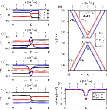
FIG. 3. Calculated low energy band properties (symbols) for SLG/Bi
2Se
3for 1 QL, with a fit to the model Hamiltonian H
SLG(solid lines). (a)–(d) The spin expectation values of the four low
energy bands. (e) The low energy band structure of proximitized
SLG. The color is the s
zexpectation value. Letters A and B indicate
the pseudospin of the bands at the K point. (f) The splitting of the
valence (conduction) band in blue (red).
TABLE I. Fit parameters of Hamiltonian H
SLGfor the SLG/Bi
2Se
3stacks for different number of QLs. The Fermi velocity v
F, gap parameter , Rashba SOC parameter λ
R, intrinsic SOC parameters λ
AIand λ
BI, and PIA SOC parameters λ
APIAand λ
BPIA. The Dirac point energy E
D, as defined in Fig. 2(a).
QLs v
F/ 10
5(m / s) ( μ eV) λ
R(meV) λ
AI(meV) λ
BI(meV) λ
APIA(meV) λ
BPIA(meV) E
D(meV)
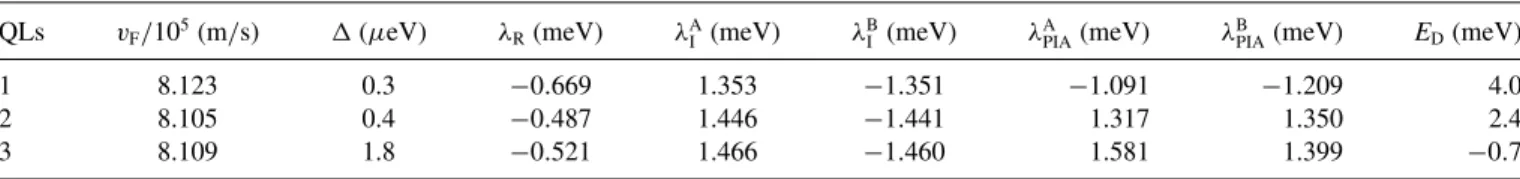
1 8.134 0.6 − 0 . 771 1.142 − 1 . 135 0.465 0.565 353.2
2 8.131 1.1 −0.691 1.221 −1.211 1.834 1.733 352.1
3 8.126 0.4 − 0 . 827 1.343 − 1 . 330 2.904 2.976 509.1
1
a8.110 21.32 −0.799 1.638 −1.517 2.708 2.433 341.2
a
With additional hBN above SLG, parameter in meV.
In Fig. 3 we show the low energy band properties for SLG/Bi
2Se
3for 1 QL, with a fit to the model Hamilto- nian. We find that the model dispersion, energy splittings, and spin expectation values agree very well with the first- principles data. In Table I we summarize the fit parameters of Hamiltonian H
SLGfor the SLG/Bi
2Se
3stacks for a dif- ferent number of QLs. We find that the fit parameters are almost independent on the number of QLs, indicating that only the closest QL is mainly responsible for proximity SOC.
However, the intrinsic SOC parameters gradually increase from about 1.1 meV for 1 QL, to 1.3 meV for 3 QLs. Such an increasing (and saturating) behavior of the induced SOC, with respect to the number of QLs, has already been reported for other interface configurations, yielding much larger SOC parameters [77]. Also the PIA SOC parameters increase with the number of QLs, while the Rashba SOC stays roughly the same. Similar to SLG/TMDC heterostructures [47,48], we find staggered intrinsic SOC, i.e., λ
AI≈ −λ
BI. In analogy to the SLG / WSe
2heterostructure [48,78], we find an inverted band structure, as the gap , being in the μ eV range, is much smaller than the spin splittings of the bands. As a consequence, SLG proximitized by the topological insulator could host protected pseudohelical states [78]. All our results are in agreement with a recent study of SLG on 1 QL of Bi
2Se
3[39]. In particular, the SOC parameters are of the same magnitude (1 meV) and are also of valley-Zeeman type, for their “large unit cell” calculation. In addition, we have calculated a heterostructure consisting of hBN/SLG/Bi
2Se
3for 1 QL, which is especially interesting for comparison to experimental studies where graphene is protected by the insulating hBN and proximitized by the topological insulator.
The fit parameters are summarized in Table I. In agreement with Ref. [73], the orbital gap parameter of the proximitized SLG is about 20 meV, much larger than for the case without hBN. Also the intrinsic SOC is a bit larger, while the rest of the fit parameters are barely different.
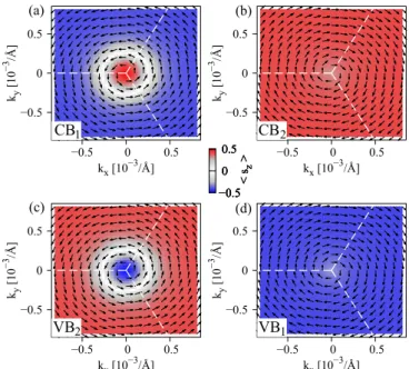
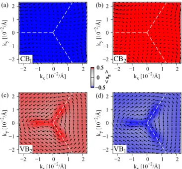
To further analyze the low energy bands, we have cal- culated the spin-orbit fields, see Fig. 4, of the four low energy bands ε
1VB/CB/2, corresponding to Fig. 3(e). The spin- orbit fields of the two outer (inner) bands rotate clockwise (counterclockwise), being a clear signature of Rashba SOC.
The spin-orbit fields are isotropic around the K point and show no signs of trigonal warping. Only the two inner bands change their s
zexpectation value, due to the inverted band structure.
The induced spin-orbit fields point out-of-plane, while the topological insulator surface states have in-plane spin-orbit fields.
As a comparative case, we also show the calculated spin- orbit fields for graphene above 3 QLs, see Fig. 5, where the PIA SOC parameters are significantly larger, see Table I, than in the 1 QL case. However, comparing the 1 QL and 3 QL cases, we do not notice any difference in the spin-orbit fields, as the magnitude (meV) of PIA SOC is still comparable in the two cases, and the other SOC parameters are almost unchanged. Only a much larger PIA SOC can significantly change the low energy band properties [72].
B. Bilayer graphene
In Fig. 6 we show the full band structures of BLG above one, two, and three QLs of Bi
2Se
3. At the K point, one can recognize the parabolic bands originating from bare BLG [76], while at the point, the surface states of the topolog- ical insulator form, just as for the SLG case. By gradually increasing the number of QLs, the Dirac bands of Bi
2Se
3start to form. The BLG bands exhibit a sizable band gap.
Additionally, the BLG gets hole doped by about 200 meV, for
(a) (b)
(c) (d)
−0.5 0 0.5
kx[10−3/Å]
−0.5 0 0.5
ky[10−3 /Å]
−0.5 0 0.5
< sz> −0.5 0 0.5
kx[10−3/Å]
−0.5 0 0.5
ky[10−3/Å]
−0.5 0 0.5
< sz>
−0.5 0 0.5
kx[10−3/Å]
−0.5 0 0.5
ky[10−3 /Å]
−0.5 0 0.5
< sz>
−0.5 0 0.5
kx[10−3/Å]
−0.5 0 0.5
ky[10−3/Å]
−0.5 0 0.5
< sz>
CB
1CB
2VB
2VB
1FIG. 4. First-principles calculated spin-orbit fields around the K
point of the bands (a) ε
1CB, (b) ε
CB2, (c) ε
VB2, and (d) ε
VB1, for the
SLG / Bi
2Se
3stack with 1 QL, corresponding to the four low energy
bands in Fig. 3(e). The dashed white lines represent the edge of the
Brillouin zone.
−0.5 0 0.5 kx[10−3/Å]
−0.5 0 0.5
ky[10−3/Å]
−0.5 0 0.5
< sz> −0.5 0 0.5
kx[10−3/Å]
−0.5 0 0.5
ky[10−3 /Å]
−0.5 0 0.5
< sz>
−0.5 0 0.5
kx[10−3/Å]
−0.5 0 0.5
ky[10−3/Å]
−0.5 0 0.5
< sz>
−0.5 0 0.5
kx[10−3/Å]
−0.5 0 0.5
ky[10−3 /Å]
−0.5
0 < s>z
(a) (b)
(c) (d)
CB
1CB
2VB
2VB
1FIG. 5. First-principles calculated spin-orbit fields around the K point of the bands (a) ε
CB1, (b) ε
2CB, (c) ε
VB2, and (d) ε
1VB, for the SLG / Bi
2Se
3stack with 3 QLs. The dashed white lines represent the edge of the Brillouin zone.
one and two QLs, whereas the Fermi level is in the band gap of BLG for 3 QLs. Experiments have reported about 380 meV of hole doping in BLG on Bi
2Se
3[54], which may be attributed to the additional SiO
2substrate.
In Fig. 7 we show the low energy band properties for BLG / Bi
2Se
3for 1 QL, with a fit to the model Hamiltonian H
BLG. As for the SLG case, we find very good agreement of our model and the first-principles dispersion, energy split- tings, and spin expectation values for the proximitized BLG.
In contrast to SLG, the BLG exhibits a large band gap of about 80 meV. As a consequence of the Bi
2Se
3substrate, and the resulting induced dipole field, the two graphene layers are at a different potential V . Since the low energy bands are
−0.5 0 0.5
M ← K → Γ
3 2 1 0 1 2 3
VB1
k [10−2/Å]
−0.5 0 0.5
M ← K → Γ
3 2 1 0 1 2 3
VB2
k [10−2/Å]
−0.5 0 0.5
M ← K → Γ
3 2 1 0 1 2 3
CB1
k [10−2/Å]
−0.5 0 0.5
M ← K → Γ
3 2 1 0 1 2 3
CB2
k [10−2/Å]
sx sy sz
120 140 160 180 200 220 240 260
M ← K → Γ
4 3 2 1 0 1 2 3
E − EF[meV]
k [10−2/Å]
DFT Model
−0.5 0 0.5
< sz>
0 0.5 1 1.52 2.5
M ← K → Γ
3 2 1 0 1 2 3
splitting [meV]
k [10−2/Å]
∆ECB
∆EVB
(a)
(b)
(c)
(d)
(e)
(f)
VB1 VB2
CB1 CB2
FIG. 7. Calculated low energy band properties (symbols) for BLG / Bi
2Se
3for 1 QL, with a fit to the model Hamiltonian H
BLG(solid lines). (a)–(d) The spin expectation values of the four low energy bands. (e) The low energy band structure of proximitized BLG. The color is the s
zexpectation value. (f) The splitting of the valence (conduction) band in blue (red).
formed by the nondimer carbon atoms of BLG, a band gap opens. In this case, the low energy conduction band is formed by the graphene layer closer to the Bi
2Se
3. The reason is that the conduction band is strongly spin split (2 meV) around the K point, due to proximity induced SOC. Since proximity induced phenomena are short range effects, only the closest graphene layer is affected. The band structure of BLG on Bi
2Se
3is very similar to the one of BLG on WSe
2[52], where a spin-orbit valve effect has been proposed.
−1
−0.5 0 0.5 1
M K Γ M
E − EF[eV]
−0.5 0 0.5
< sz>
−1
−0.5 0 0.5 1
M K Γ M
E − EF[eV]
(a) (b) (c)
ED
ETI
−1
−0.5 0 0.5 1
M K Γ M
E − EF[eV]
FIG. 6. Calculated band structures of BLG on (a) one, (b) two, and (c) three QLs of Bi
2Se
3. The color is the s
zexpectation value. In (a) we
define the Dirac point energy E
Dand the doping energy of the topological insulator E
TI.
TABLE II. Fit parameters of Hamiltonian H
BLGfor the BLG/Bi
2Se
3stacks for different number of QLs. Intra- and interlayer hoppings γ of the BLG, when the lower (upper) GRP layer is placed in potential V ( − V ). The asymmetry in the energy shift of the bonding and antibonding states . Intrinsic SOC parameters of the corresponding layer and sublattice λ
I. Global and local space inversion symmetry breaking SOC parameters λ
0and λ
R.
γ
0γ
1γ
3γ
4V λ
A1Iλ
B1Iλ
A2Iλ
B2Iλ
0λ
RE
DQLs (eV) (meV) (meV) (meV) (meV) (meV) (meV) (meV) (meV) (meV) (meV) (meV) (meV)
1 2.513 373.5 − 274 . 9 − 165 . 3 41.60 13.79 − 1 . 056 1.170 0.012 0.012 − 0 . 433 − 0 . 273 183.3
2 2.512 373.5 −275.5 −165.6 43.12 13.79 −1.117 1.301 0.012 0.012 −0.167 −0.199 181.4
3 2.513 373.9 − 264 . 9 − 163 . 5 23.63 13.54 − 1 . 030 1.168 0.012 0.012 − 0 . 190 − 0 . 188 19.95
In Table II we summarize the fit parameters of Hamiltonian H
BLGfor the BLG/Bi
2Se
3stacks for a different number of QLs. We find that the fit parameters are almost independent on the number of QLs, indicating that only the closest QL is mainly responsible for proximity SOC, similar to what we have found from the SLG case. For the fit we assume for simplicity the pristine graphene intrinsic SOC parameters [46] for the top layer ( λ
A2I= λ
B2I= 12 μ eV). In agreement with the monolayer case, we find staggered intrinsic SOC, i.e., λ
A1I≈ −λ
B1I. Consequently, also proximitized BLG can exhibit topologically protected phases, as recently shown [79].
Surprisingly, the gap parameter V diminishes by about 50%, for 3 QLs and the Fermi level is now located within the band gap of the BLG.
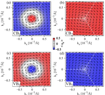
By looking at the calculated spin-orbit fields, see Fig. 8, we find that the two proximity spin-orbit split conduction bands are strongly s
zpolarized. In contrast, the two valence bands exhibit a typical Rashba type spin-orbit field. In the case of SLG on TMDCs, the induced strong staggered SOC (opposite sign on the two sublattices) seems to be a consequence of
−2 −1 0 1 2
kx[10−2/Å]
−2
−1 0 1 2
ky[10−2/Å]
−0.5 0 0.5
<sz> −2 −1 0 1 2
kx[10−2/Å]
−2
−1 0 1 2
ky[10−2 /Å]
−0.5 0 0.5
<sz>
−2 −1 0 1 2
kx[10−2/Å]
−2
−1 0 1 2
ky[10−2/Å]
−0.5 0 0.5
<sz>
−2 −1 0 1 2
kx[10−2/Å]
−2
−1 0 1 2
ky[10−2 /Å]
−0.5 0 0.5
<sz>
(a) (b)
(c) (d)
CB
1CB
2VB
2VB
1FIG. 8. First-principles calculated spin-orbit fields around the K point of the bands (a) ε
CB1, (b) ε
CB2, (c) ε
2VB, and (d) ε
1VB, for the BLG / Bi
2Se
3stack with 1 QL, corresponding to the four low energy bands in Fig. 7(e). The dashed white lines represent the edge of the Brillouin zone.
the s
zpolarized spin-valley locked states from the TMDC, getting imprinted on the SLG (or BLG). In our investigated case, the surface states of the topological insulator have spin- momentum locking, however with in-plane (s
xand s
y) spin components. Still, the induced spin-orbit fields are out-of- plane, similar to the SLG/TMDC case.
So far there is no complete microscopic understanding why in these two cases (SLG / Bi
2Se
3and SLG / TMDC) the induced SOC is of valley-Zeeman type. However, in the case of SLG/TMDC structures, there are already first approaches discussing how the induced SOC depends on the twist angle and the position of the SLG Dirac point with respect to the TMDC band edges [22].
V. TRANSVERSE ELECTRIC FIELD
We have seen that the parameters and proximity SOC are marginally affected by adding more QLs. We now study the effect of a transverse electric field only for 1 QL of Bi
2Se
3. Can we tune proximity SOC by the electric field? Is a spin- orbit valve effect present in BLG?
A. Graphene
In Fig. 9 we show the fit parameters of Hamiltonian H
SLGfor the SLG/Bi
2Se
3stack as a function of a transverse electric field. We find that the dipole of the structure grows linearly with applied electric field. The Fermi velocity v
Fis only slightly affected by the field, but shows a linear dependence.
The gap parameter , reflecting the sublattice symmetry breaking, stays tiny in magnitude without any noticeable trend. The intrinsic as well as Rashba SOC parameters grow in magnitude, when changing the field from negative to positive amplitude. While the intrinsic SOC parameters, λ
AIand λ
BI, can be changed from about 1 to 1.2 meV, the Rashba SOC parameter λ
Rchanges from about 0.6 to 0.9 meV in magni- tude, when tuning the electric field from −2.5 to 2.5 V/nm.
A roughly linear trend can also be observed in the PIA SOC
parameters, which can be tuned from 0 up to 0.8 meV. The
Dirac point energy E
Dstays at the same position, with respect
to the Fermi level, as the field changes. The doping energy
of the topological insulator E
TIdecreases, when a negative
electric field is applied. Such a field tunability of the SOC
parameters, especially the Rashba one, can lead to a giant
control of spin relaxation times and anisotropies in SLG
[39,73].
0 0.2 0.4 0.6 0.8 1
−2 −1 0 1 2
∆[μeV]
electric field [V/nm]
−1 0 1
−2 −1 0 1 2
param [meV]
electric field [V/nm]
λR λIA λIB
8.13 8.135 8.14
−2 −1 0 1 2
vF[105m/s]
electric field [V/nm]
0 0.2 0.4 0.6 0.8
−2 −1 0 1 2
param [meV]
electric field [V/nm]
λPIAA λPIAB
−10
−5 0 5 10 15
−2 −1 0 1 2
dipole [debye]
electric field [V/nm]
0 100 200 300 400
−2 −1 0 1 2
energy [meV]
electric field [V/nm]
ED
−ETI (a)
(b)
(c)
(d)
(e)
(f)
FIG. 9. Fit parameters of Hamiltonian H
SLGfor the SLG / Bi
2Se
3stack with 1 QL as a function of a transverse electric field. (a) The gap parameter , (b) the Fermi velocity v
F, (c) the dipole of the structure, (d) Rashba SOC parameter λ
R, intrinsic SOC parameters λ
AIand λ
BI, (e) PIA SOC parameters λ
APIAand λ
BPIA, and (f) the Dirac point energy E
Dand the doping energy of the topological insulator E
TI, as defined in Fig. 2(a).
B. Bilayer graphene
Most interesting is the case of BLG under the influence of an electric field. As already mentioned, the band structure is very similar to the one of BLG on WSe
2[52], where a spin-orbit valve effect has been proposed. In Fig. 10 we show the fit parameters of Hamiltonian H
BLGfor the BLG/Bi
2Se
3stack as a function of a transverse electric field. We find that the dipole of the structure grows linearly with applied electric field, similar to the SLG case. Most of the orbital and spin- orbit parameters stay more or less constant as a transverse electric field is applied. However, the field can for example tune the doping energy of the topological insulator E
TI, and also slightly tune the interlayer hopping amplitude γ
3.
Surprisingly, the parameter λ
0drastically decreases in magnitude for positive fields. This means that the electric field, felt by one graphene layer due to the presence of the other, in this proximity effect setup, diminishes with applied external transverse field. Important for the previously men- tioned spin-orbit valve effect is the closing of the orbital gap, and the subsequent reopening with inverted band structure.
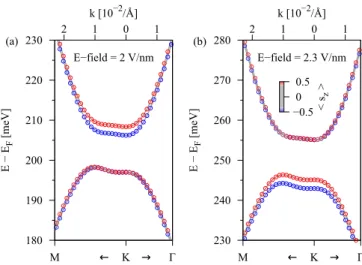
Indeed, such a situation can be realized, for a transverse electric field around 2.1 V/nm, as the two graphene layers are at the same potential, when the paramter V goes through zero.
For an electric field of 2 V / nm, the band structure is shown in Fig. 11(a). The orbital gap of the BLG bands is about 10 meV, and the conduction band is strongly spin-orbit split. For a field of 2.3 V/nm, the band structure is inverted, see Fig. 11(b), and the valence band is now strongly spin-orbit split. The spin- orbit split bands are always localized on the graphene layer closest to the substrate. In Fig. 11(f) we can see that the band splittings near the K point for conduction and valence band
0 20 40 60 80
−1 0 1 2
param [meV]
electric field [V/nm]
γ0/100
∆ V
−1 0 1
−1 0 1 2
param [meV]
electric field [V/nm]
λIA1 λIB1
−400
−300
−200
−1 0 1 2
param [meV]
electric field [V/nm]
−γ1 γ3 γ4
−0.4
−0.2 0
−1 0 1 2
param [meV]
electric field [V/nm]
λ0 λR
−5 0 5 10 15
−1 0 1 2
dipole [debye]
electric field [V/nm]
100 150 200 250 300
−1 0 1 2
energy [meV]
electric field [V/nm]
ED −ETI
(a)
(b)
(c)
(d)
(e)
(f)
FIG. 10. Fit parameters of Hamiltonian H
BLGfor the BLG/Bi
2Se
3stack with 1 QL as a function of a transverse electric field. (a) The nearest neighbor hopping parameter γ
0, the asymmetry in the energy shift of the bonding and antibonding states , and the SLG layer potential V . (b) The intra- and interlayer hoppings γ
1, γ
3, and γ
4. (c) The dipole of the structure. (d) The two proximity modified intrinsic SOC parameters λ
A1Iand λ
B1I. (e) The global and local space inversion symmetry breaking SOC parameters λ
0and λ
R. (f) The Dirac point energy E
Dand the doping energy of the topological insulator E
TI, as defined in Fig. 6(a).
differ by orders of magnitude. Important for the spin-orbit valve effect is that spin relaxation depends quadratically on the magnitude of the band splittings. Consequently, the spin relaxation for electrons (holes) is large (small) for an electric field of about 2 V/nm, and vice versa for a field of about 2.3 V/nm.
(a) (b)
180 190 200 210 220 230
M ← K → Γ
2 1 0 1
E − EF[meV]
E−field = 2 V/nm k [10−2/Å]
−0.5 0 0.5
< sz>
230 240 250 260 270 280
M ← K → Γ
2 1 0 1
E − EF[meV]
E−field = 2.3 V/nm k [10−2/Å]
FIG. 11. Calculated low energy bands for BLG / Bi
2Se
3for 1 QL,
with applied transverse electric field of (a) 2 V/nm and (b) 2.3 V/nm.
0 1 2 3 4
3.2 3.4 3.6 3.8
∆[μeV]
distance [Å]
−2 0 2
3.2 3.4 3.6 3.8
param [meV]
distance [Å]
λR λIA λIB
8.05 8.1 8.15
3.2 3.4 3.6 3.8
vF[105m/s]
distance [Å]
0 0.2 0.4 0.6
3.2 3.4 3.6 3.8
param [meV]
distance [Å]
λPIAA
λPIAB
0 100 200 300
3.2 3.4 3.6 3.8
Etot− E0[meV]
distance [Å]
100 200 300 400
3.2 3.4 3.6 3.8
energy [meV]
distance [Å]
ED −ETI (a)
(b)
(c)
(d)
(e)
(f)
FIG. 12. Fit parameters of Hamiltonian H
SLGfor the SLG/Bi
2Se
3stack with 1 QL as a function of the interlayer distance. (a) The gap parameter , (b) the Fermi velocity v
F, (c) the total energy with respect to the minimal energy E
0, (d) Rashba SOC parameter λ
R, intrinsic SOC parameters λ
AIand λ
BI, (e) PIA SOC parameters λ
APIAand λ
BPIA, and (f) the Dirac point energy E
Dand the doping energy of the topological insulator E
TI, as defined in Fig. 2(a).
VI. ADDITIONAL CONSIDERATIONS
Our DFT calculations, together with the extracted fit pa- rameters, can give an insight on the magnitude of the induced SOC in SLG, and are helpful to analyze and interpret experi- mental data in SLG/topological insulator heterostructures, as recently proven [39,41]. However, there are still some open questions that we would like to address in the following. Is the chosen interlayer distance of 3.5 Å reasonable for the studied heterostructures? How does proximity SOC depend on
it? How does the proximity SOC depend on the composition of the topological insulator? Can we tune the Dirac states of SLG down to the Fermi level, by using a different topological insulator?
A. Distance study
It has been shown that proximity SOC and exchange effects can be significantly enhanced when decreasing the interlayer distance between materials [73,80–82]. Here we look into the proximity effects, when we modify the interlayer distance between SLG and Bi
2Se
3. Similar results can be expected for the BLG case.
In Fig. 12 we show the fit parameters of Hamiltonian H
SLGfor the SLG/Bi
2Se
3stack with 1 QL as a function of the interlayer distance between SLG and Bi
2Se
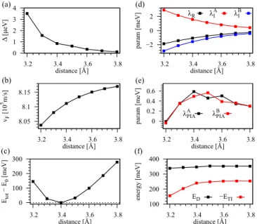
3. Our study shows that the lowest energy is achieved for an interlayer distance of 3.4 Å, very close to our chosen distance of 3.5 Å according to Ref. [39]. Note that the energetically most favorable interlayer distance depends on the specific DFT input and the chosen vdW corrections. The proximity induced intrinsic and Rashba SOC parameters show the expected behavior and decrease in magnitude, as we increase the interlayer distance, see Fig. 12(d). The increase of the parameters is giant, about 200% when we decrease the interlayer distance by only about 10%.
Surprisingly, the PIA SOC parameters first increase with increasing the interlayer distance from 3.2 to 3.4 Å. A possible explanation might be the position of the SLG Dirac point with respect to the bands of the topological insulator. Looking at the band structure Fig. 2(a), we see that there are bands of the topological insulator anticrossing with the SLG Dirac bands, at around 0.6 eV. With increasing the distance, the Dirac point of SLG stays roughly at the same energy, while the bands of the topological insulator shift down in energy;
compare the energies E
Dand E
TIin Fig. 12(f). Consequently, the anticrossing bands move closer towards the SLG Dirac point and we need a larger PIA parameter to capture the low energy bands. For interlayer distances, larger than 3.4 Å, the
(a) (b) (c)
ED
ETI
−1
−0.5 0 0.5 1
M K Γ M
E − EF[eV]
−0.5 0 0.5
< sz>
−1
−0.5 0 0.5 1
M K Γ M
E − EF[eV]
−1
−0.5 0 0.5 1
M K Γ M
E − EF[eV]