Swapping exchange and spin-orbit coupling in ex-so-tic 2D heterostructures
Klaus Zollner,1,∗ Martin Gmitra,2 and Jaroslav Fabian1
1Institute for Theoretical Physics, University of Regensburg, 93053 Regensburg, Germany
2Institute of Physics, P. J. ˇSaf´arik University in Koˇsice, 04001 Koˇsice, Slovakia (Dated: May 25, 2020)
The concept of swapping the two most important spin interactions—exchange and spin-orbit coupling—is proposed based on two-dimensional multilayer van der Waals heterostructures. Specif- ically, we show by performing realistic ab initio simulations, that a single device consisting of a bilayer graphene sandwiched by a 2D ferromagnet Cr2Ge2Te6 (CGT) and a monolayer WS2, is able not only to generate, but also to swap the two interactions. The highly efficient swapping is enabled by the interplay of gate-dependent layer polarization in bilayer graphene and short-range spin-orbit and exchange proximity effects affecting only the layers in contact with the sandwiching materials.
We call these structuresex-so-tic, for supplying either exchange (ex) or spin-orbit (so) coupling in a single device, by gating. Such bifunctional devices demonstrate the potential of van der Waals spintronics engineering using 2D crystal multilayers.
Keywords: spintronics, graphene, heterostructures, proximity spin-orbit coupling, proximity exchange
Introduction. In the paradigmatic spintronic device, the still elusive Datta-Das spin transistor [1], the spin- orbit coupling in a thin semiconductor channel rotates the spin of electrons flowing between two ferromagnetic electrodes. The transistor relies on one crucial aspect: a gate atop the channel modifies the magnitude of the spin- orbit interaction. As a result, one could electrically tune the spin precession between say 0 and 180 degrees, and turn the electron flow on or off. While other spin transis- tor designs have since been demonstrated [2–5], the prin- cipal difficulty of controlling spin interactions via elec- tric fields remains as long as one deals with conventional semiconductor materials. Similar problems are faced by controlling exchange coupling electrically. In a pioneer- ing experiment [6] 125 V was needed to turn the magnetic moment of ferromagnetic semiconductor InMnAs on and off.
The advent of 2D van der Waals heterostructures gave a strong push to spintronics [7, 8], with well-founded hopes for a far greater control over spin interactions such as spin-orbit and exchange couplings. The key mecha- nism, allowing such a control, is an interplay of the prox- imity effect [9] and gating. The past years have seen impressive progress in this direction, for both spin-orbit and exchange couplings individually [10–21].
Bilayer graphene (BLG) is emerging as a particularly useful platform for controlling the spin interactions by proximity effects. It was proposed that spin-orbit cou- pling in BLG can be turned on and off on demand [22, 23]
by gating, as recently demonstrated by capacitance mea- surements [24]. Similar effects have been predicted for ferromagnetic encapsulation [25–27]. The next milestone would be a transport demonstration with sensitivity to the spin polarization of the bands, or the spin-orbit torque in the proximity setup [28–30].
In this paper we present a device structure which is ca- pable of not only creating the two most important spin interactions—spin-orbit and exchange couplings—in an
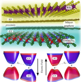
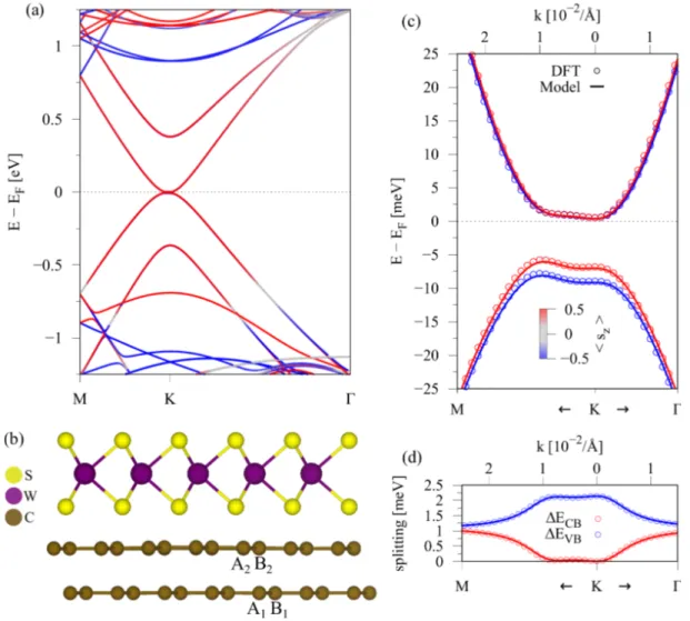
FIG. 1. Ex-so-tic van der Waals heterostructure. Top: BLG sandwiched between a monolayer TMDC (such as WS2 or MoSe2) and a monolayer ferromagnetic semiconductor (such as CGT or CrI3). The magnetization of the ferromagnet is indicated by the arrows. The top layer of BLG is proxim- itized by the TMDC, acquiring a giant spin-orbit coupling, while the bottom layer of the BLG is proximitized by the fer- romagnet, acquiring an exchange coupling. Bottom: Electric tunability of the low-energy bands atK andK0. The colors red and blue indicate out-of-plane spin. For a fixed Fermi levelEF (here in the conduction band), the Dirac electrons experience either exchange or spin-orbit coupling, depending on the electric field.
electronic system, but also swapping them on demand by an applied electric field. Being able to swap two dif- ferent spin (or other effective) interactions by gating is
arXiv:2005.11058v1 [cond-mat.mes-hall] 22 May 2020
a striking thought, without precedence in the realm of conventional materials. While proximity spin-orbit cou- pling preserves time-reversal symmetry, and leads to such phenomena as topological quantum spin Hall effect [31]
or giant spin relaxation anisotropy [15, 32–34], proxim- ity exchange coupling breaks time reversal symmetry and renders a nominally nonmagnetic electronic system effec- tively magnetic [35]. Swapping the two interactions pro- vides a reversible route between time-reversal symmetric and magnetic physics.
Our choice of the electronic platform for swapping the spin interactions is BLG, which is nicely suited for proximity-based devices by providing two coupled sur- faces. Via layer polarization, which locks a given layer to an electronic band (or set of bands), transport properties can be strongly influenced by the environment. We use a CGT/BLG/WS2heterostructure, with monoloayer CGT providing a strong proximity exchange effect to the bot- tom layer of BLG, and WS2 to induce strong spin-orbit coupling to the top layer, see Fig. 1. Both CGT and WS2are semiconductors, so they contribute to transport properties of the heterostructure only by imprinting their characteristic spin properties onto the BLG.
Gating can swap spin-orbit and exchange couplings, as illustrated in Fig. 1. The applied electric field changes the layer polarization, which changes the layer-band as- signment, thereby swapping the proximity exchange and spin-orbit couplings. This intuitive picture is supported below by realistic density functional theory (DFT) simu- lations and phenomenological modeling, predicting quan- titatively the behavior of the ex-so-tic heterostructures in the presence of a transverse electric field.
Swapping spin-orbit and exchange coupling by gate.
We consider a supercell stack containing BLG sand- wiched between a monolayer WS2 and a monolayer fer- romagnetic CGT with an out-of-plane magnetization, as depicted in Fig. 1. We calculate the electronic states for this structure using DFT, see Supplemental Material [36]. The band structure along selected high-symmetry lines containing K point is shown in Fig. 2. The magnetization—from CGT—as well as the strong spin- orbit coupling—from TMDC—are manifested by the spin polarization of the bands. Inside the semiconductor band gap, there are well preserved parabolic electronic states of BLG. States relevant for transport form the four low- energy bands close to the Fermi level. It is these four bands that are at the focus of this work.
BLGper sehas no band gap, has tiny spin-orbit cou- pling (on the order of tens of µeVs [37]), and has no magnetic exchange coupling. But sandwiched by the two monolayers, both orbital and spin properties of the low- energy bands of BLG strikingly change. First, the built- in dipole moment in the heterostructure [22, 27] separates conduction and valence bands, inducing a band gap for a given spin polarization. Next, the states exhibit a gi- ant spin-orbit coupling induced from the TMDC layer.
−1
−0.5 0 0.5 1
M K Γ
E − EF[eV]
1 0 1 2
k [10−2/Å]
← K → Γ
1 0 1 2
k [10−2/Å]
← K → Γ
1 0 1 2
k [10−2/Å]
−20
−10 0 10 20
M ← K →
E − EF[meV]
−0.5 0 0.5
< sz>
4
6 2 1 0 1
ing [meV]
k [10−2/Å]
∆EC FIG. 2. Calculated electronic band structure of a WS2/BLG/CGT stack along high symmetry path M-K-Γ.
The color of bands (red and blue) corresponds to thesz spin expectation value.
This coupling is opposite inK andK0 points, as a con- sequence of time reversal symmetry of the spin-orbit in- teraction. Finally, the electronic states of BLG become magnetic, manifested by an exchange splitting, equal in K and K0, coming from the ferromagnetic CGT. It is the fascinating spectral separation of the spin-orbit cou- pling and exchange in the BLG which allows for their swapping.
The three aforementioned effects are nicely seen in Fig.
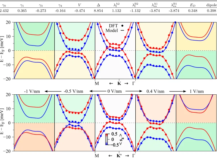
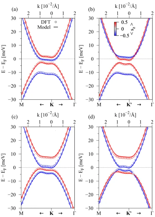
3 which shows a zoom to the low-energy band structure of the stack at bothK andK0. Perhaps the most strik- ing feature of the band structure is the difference in the energy dispersion atK andK0, which ultimately comes from the interplay between the induced spin-orbit and exchange couplings in BLG. While the valence and con- duction bands partially overlap at K, there is a local band gap atK0. The dipole moment of the heterostruc- ture is too weak to open a global (over the whole Brillouin zone) band gap. The spin splittings are 2–8 meV, which is experimentally significant.
An applied external electric field increases the band gap of the doubly proximitized BLG and makes explicit the effects of the TMDC and CGT layers. This is demon- strated in Fig. 3, which shows both the DFT results (for fields −0.5, 0, and 0.4 V/nm) and model calculations (for fields, −1, −0.5, 0, 0.4, and 1 V/nm) using an ef- fective Hamiltonian introduced in the next section. Let us first look at negative electric fields, say −1 V/nm, which point down, towards CGT. The conduction bands are split by about 8 meV, having identical spin polariza- tions atKandK0, which means that this splitting is due to exchange coupling: the conduction bands are affected
3
TABLE I. Parameters of the model Hamiltonian H, Eq. (1), fitted to the DFT low-energy dispersion data for the CGT/BLG/WS2 heterostructure at zero applied electric field. Parametersγ are in eV, others in meV. The dipole is given in debye. Unspecified model parameters are zero. Based on the fit parameters for the individual BLG/CGT and WS2/BLG subsystems given in the Supplementary Information, we assumedλA2I =−λB2I andλA1ex =λB1ex here for the fit.
γ0 γ1 γ3 γ4 V ∆ λA2I λB2I λA1ex λB1ex ED dipole
2.432 0.365 -0.273 -0.164 -0.474 8.854 1.132 -1.132 -3.874 -3.874 0.348 0.398
−20
−10 0 10 20
E − E
F[meV]
−20
−10 0 10 20
E − E
F[meV]
M ← K → Γ
Model DFT
−0.5 0 0.5
< s
z>
M ← K' → Γ
−0.5 0 0.5
< s
z>
−0.5 0 0.5
< s
z>
−0.5 0 0.5
< s
z>
−0.5 0 0.5
< s
z>
−0.5 0 0.5
< s
z>
-1 V/nm -0.5 V/nm 0 V/nm 0.4 V/nm 1 V/nm
FIG. 3. Low energy dispersion curves around K (top) and K’ (bottom) for the WS2/BLG/CGT heterostructure. The color of the curves corresponds to thesz spin expectation value: spin up is red and spin down is blue. The yellowish and reddish backgrounds indicate that the bands are split by spin-orbit coupling: the yellowish is for down-up (blue-red) and reddish for up-down (red-blue) spin ordering along increasing energy. The greenish background is for exchange coupling whose ordering is always up-down, fixed by the magnetization of the CGT layer. From left to right the transverse electric field is tuned from
−1 to 1 V/nm. For electric fields of−0.5, 0, and 0.4 V/nm both model (solid lines) and DFT data (symbols) are plotted. For electric fields of±1 V/nm we use the model parameters with extrapolated values forV, assuming a linear dependence on the field. ParametersV = 7.1, 3.2,−0.5,−3.6,−8.1 meV correspond to the field values of−1,−0.5, 0, 0.4, 1 V/nm, respectively.
by the ferromagnetic CGT and conduction electrons will exhibit transport properties of magnetic conductors. On the other hand, the valence bands are split less, by about 2 meV. More important, the spin polarizations of the two bands are opposite atK andK0, signaling time-reversal symmetry: the valence bands experience spin-orbit cou- pling from WS2. This makes sense. At negative electric fields electrons in the upper layer of BLG have a lower energy, and form the valence band. These electrons are affected by the TMDC layer, which gives them the strong spin-orbit coupling character. We will see in the next sec-
tion that the spin-orbit coupling is of the valley Zeeman type, which is characteristic for graphene proximitized by a TMDC. Similarly, electron orbitals in the lower layer of BLG have a higher energy, forming the conduction band, which is magnetic due to the presence of CGT.
If the applied electric field points up, towards the TMDC layer, the situation is reversed, see Fig. 3. While the orbital band gap develops again, the spin charac- ters of the valence and conduction bands are swapped.
The conduction bands are now split by spin-orbit cou- pling, and the valence bands by strong exchange cou-
pling. The reason is that the conduction bands are now formed by orbitals from the upper BLG layer which is close to TMDC, and the valence bands by orbitals from the lower BLG layer, close to the magnetic CGT.
We have thus demonstrated the swapping of exchange and spin-orbit couplings: at a fixed chemical potential (doping level), the investigated electronic system exhibits exchange coupling at one value of the electric field, and spin-orbit coupling at another. This gating effect con- trols the spin character of the states, and effectively turns time reversal symmetry on (spin-orbit coupling) or off (exchange). Such ex-so-tic structures offer on-demand exchange and spin-orbit coupling.
It is not essential for the swapping operation that the BLG is sandwiched between monolayers. Few-layer TMDCs and ferromagnets would work equally well. The short-rangeness of the proximity effect acts both ways.
For example, the CGT monolayer induces exchange cou- pling to the adjacent (here lower) layer of BLG. The up- per BLG layer is affected much less. Adding more layers of CGT will not matter. It will still be the interfacial layer which hybridizes with the carbon orbitals and in- duces the exchange in BLG. This picture was demon- strated explicitly by systematic DFT investigations in few-layer TMDC/CrI3 slabs [38].
Model Hamiltonian. We now describe the low-energy band structure of the doubly proximitized BLG in the vicinity of K and K’ valleys using an effective model that captures the essential physics. For this purpose we em- ploy a Hamiltonian which was originally derived from symmetry arguments for AB stacked BLG in the pres- ence of an external transverse electric field [37]. In our case the extrinsic effects are caused by the heterostruc- ture: the upper BLG layer is proximitized by the TMDC, while the lower layer by the ferromagnetic CGT. Beyond these adjacent layers the proximity effect is too weak to markedly affect the band structure of BLG, which is also explicitly demonstrated by our study of individual TMDC/BLG and BLG/CGT bilayers (see Supplemental Material [36]).
The effective Hamiltonian reads
H=Horb+Hsoc+HR+Hex+ED. (1)
It comprises orbital (orb), intrinsic spin-orbit (soc), Rashba (R), and exchange (ex) terms. We also include the Dirac-point energyED, which is a global energy shift to offset charge transfer in DFT results. In what fol- lows we specify the individual Hamiltonian terms using pseudospin notation in which the physics is particularly transparent. A matrix form ofHis given in Supplemen- tal Material [36].
The orbital physics is captured by Horb=−
√3γ0a
2 µ0⊗(τ kxσx+kyσy)⊗s0
+γ1
2(µx⊗σx−µy⊗σy)⊗s0
−
√3γ3a
4 µx⊗(τ kxσx−kyσy)⊗s0
−
√3γ3a
4 µy⊗(τ kxσy+kyσx)⊗s0
−
√3γ4a
2 (τ kxµx−kyµy)⊗σ0⊗s0
+V µz⊗σ0⊗s0
+ ∆(µ+⊗σ++µ−⊗σ−)⊗s0, (2) where we denote the graphene lattice constantaand the Cartesian components of the wave vectorkxandky mea- sured from±K for the valley indexτ =±1. The Pauli matricesµi,σi, andsi, represent layer, pseudospin, and spin, withi={0, x, y, z}. We also defineµ±= 12(µz±µ0) andσ±= 12(σz±σ0) to shorten notation. Parametersγj, j={0,1,3,4}, describe intra- and interlayer hoppings of the BLG. To describe the effect of a transverse displace- ment field we introduce the voltage parameterV for the lower, and−V for the upper layer of BLG. The parame- ter ∆ describes the asymmetry in the energy shift of the bonding and antibonding states.
The proximity effects dramatically influence the spin states via spin-orbit coupling. The intrinsic spin-orbit coupling term, while also present in a free-standing BLG, is strongly renormalized by the proximity to the TMDC.
This effect is described by
Hsoc=µ+⊗τ(λA1I σ++λB1I σ−)⊗sz
−µ−⊗τ(λA2I σ++λB2I σ−)⊗sz, (3) with parameters λI denoting the proximity spin-orbit coupling of the corresponding layer (1,2) and sublattice (A, B) atom. Due to the short-rangeness of the proximity effect only the upper layer, so that only parametersλA2I andλB2I are significant (on the meV scale). The Rashba coupling can emerge due to the breaking of the space in- version symmetry in the heterostructure and the applied electric field. This term has the form
HR= 1
2(λ0µz+ 2λRµ0)⊗(τ σx⊗sy−σy⊗sx), (4) whereλ0describes the local (intrinsic) breaking of space inversion due to the presence of the other layer in BLG.
The resulting spin-orbit fields are opposite in the two lay- ers, giving no net effect on the spin-orbit splitting. The global breaking of space inversion due to the heterostruc- ture and the electric field is accounted for by the proper Rashba parameterλR. For a more detailed description of the model and parameters, we refer the reader to Ref.
5 [37]. Finally, the magnetic proximity effect induces ex-
change coupling in BLG, which has the standard form, Hex=µ+⊗(−λA1exσ++λB1exσ−)⊗sz
−µ−⊗(−λA2exσ++λB2exσ−)⊗sz, (5) where parameters λexrepresent the proximity exchange for the individual sublattices and layers.
The spectrum of the effective Hamiltonian H is fit- ted to the DFT-obtained low-energy dispersion of doubly proximitized BLG at zero applied electric field shown in Fig. 2. First, the orbital parameters γj from Horb are obtained, as well as the built-in biasV, staggered poten- tial ∆, and the Dirac energyED. In the second step we analyze the fine structure of the spectrum and extract proximity induced spin-orbit and exchange parameters.
The induced spin-orbit coupling in the upper layer is of the valley-Zeeman type, with opposite parameters on the two atoms of the sublattice: λA2I = −λB2I ≈ 1.1 meV.
The atoms of the lower BLG layer experience strong proximity exchange coupling due to the adjacent CGT, λA1ex =λB1ex ≈ −3.9 meV . As for the Rashba coupling, it is negligible (on the meV scale), which is consistent with our finding that the spin polarization of the considered bands is predominantly out of plane. The fitted parame- ters are summarized in Tab. I; parameters not presented there were found to be negligible and set to zero. With such a minimal set of parameters the agreement of the effective model and the DFT is excellent, see Fig. 3.
The fitted parameters explicitly demonstrate the mes- sage that one layer of BLG experiences giant (on the meV scale) spin-orbit coupling, while the other layer giant ex- change coupling, at zero electric field. What about the spectrum at finite electric fields? The only parameter that significantly changes when a field is applied is the voltage bias V between the two layers, as the other pa- rameters are largely fixed by orbital hybridization. We therefore changeV in our model Hamiltonian (and keep other parameters as fitted to the zero-field DFT results) to see how the spectra develop. The results are presented in Fig. 3. Their qualitative interpretation was already given above. Here we only note that the consistency of this procedure (changing onlyV as the electric field is ap- plied) is checked by performing DFT simulations for two electric fields,−0.5 and 0.4 V/nm; for ±1 V/nm we use V assuming its linear dependence on the applied electric field. The agreement with the model calculations, seen in Fig. 3, gives us full confidence in our approach. More de- tailed fit results can be found in the Supplemental Mate- rial [36], where we also provide results for the individual BLG/CGT and WS2/BLG subsystems, to further vali- date the robustness of the model.
Summary. Doubly proximitized BLG offers a unique platform for investigating fundamental spin physics and designing multifunctional spintronics applications. Using realistic DFT simulations and phenomenological model-
ing we demonstrate swapping the two most important spin interactions—exchange and spin-orbit couplings—
in a WS2/BLG/CGT multilayer. The swapping also means turning the time-reversal symmetry on and off, on demand, in the electronic states at a given doping.
Since the effect is robust, we expect a variety of swap- ping phenomena if the bilayer sandwich comprises an- tiferromagnets, ferroelectricity, ferroelectrics, topological insulators, or superconductors.
This work was funded by the Deutsche Forschungsge- meinschaft (DFG, German Research Foundation) SFB 1277 (project-id 314695032), the European Unions Hori- zon 2020 research and innovation program under Grant No. 785219, DFG SPP 1666, and by the VEGA 1/0105/20 and VVGS-2019-1227.
∗ klaus.zollner@physik.uni-regensburg.de
[1] Datta, S. & Das, B. Electronic analog of the electrooptic modulator. Appl. Phys. Lett.56, 665 (1990).
[2] Schliemann, J., Egues, J. C. & Loss, D. Nonballistic Spin-Field-Effect Transistor.Phys. Rev. Lett.90, 146801 (2003).
[3] Wunderlich, J.et al.Spin Hall Effect Transistor.Science 330, 1801 (2010).
[4] Betthausen, C.et al.Spin-Transistor Action via Tunable Landau-Zener Transitions. Science 337, 324 (2012).
[5] Chuang, P.et al.All-electric all-semiconductor spin field- effect transistors. Nature Nanotechnol.10, 35 (2015).
[6] Ohno, H.et al. Electric-field control of ferromagnetism.
Nature408, 944 (2000).
[7] Han, W., Kawakami, R. K., Gmitra, M. & Fabian, J.
Graphene spintronics. Nat. Nanotechnol.9, 794 (2014).
[8] Avsar, A. et al. Colloquium: Spintronics in graphene and other two-dimensional materials. arXiv:1909.09188 (2019).
[9] Zutic, I., Matos-Abiague, A., Scharf, B., Dery, H. & Be- lashchenko, K. Proximitized materials.Mater. Today22, 85 (2019).
[10] Wang, Z. et al. Strong interface-induced spin-orbit in- teraction in graphene on WS2. Nat. Commun. 6, 8339 (2015).
[11] Avsar, A.et al. Optospintronics in Graphene via Prox- imity Coupling. ACS Nano11, 11678 (2017).
[12] Luo, Y. K. et al. Opto-valleytronic spin injection in monolayer MoS2/few-layer graphene hybrid spin valves.
Nano Lett.17, 3877 (2017).
[13] Zhong, D.et al.Layer-resolved magnetic proximity effect in van der Waals heterostructures. Nat. Nanotechnol.
(2020).
[14] Karpiak, B.et al.Magnetic proximity in a van der Waals heterostructure of magnetic insulator and graphene. 2D Mater.7, 015026 (2019).
[15] Ghiasi, T. S., Ingla-Ayn´es, J., Kaverzin, A. A.
& Van Wees, B. J. Large Proximity-Induced Spin Lifetime Anisotropy in Transition-Metal Dichalco- genide/Graphene Heterostructures. Nano Lett.17, 7528 (2017).
[16] Ghiasi, T. S., Kaverzin, A. A., Blah, P. J. & van
Wees, B. J. Charge-to-Spin Conversion by the Rashba–
Edelstein Effect in Two-Dimensional van der Waals Het- erostructures up to Room Temperature. Nano Lett.19, 5959 (2019).
[17] Ghazaryan, D.et al. Magnon-assisted tunnelling in van der Waals heterostructures based on CrBr3. Nat. Elec- tron.1, 344 (2018).
[18] Safeer, C. et al. Room-temperature spin Hall effect in graphene/MoS2 van der Waals heterostructures. Nano Lett.19, 1074 (2019).
[19] Benitez, L. A.et al.Tunable room-temperature spin gal- vanic and spin Hall effects in van der Waals heterostruc- tures. Nat. Mater.19, 170 (2020).
[20] Cort´es, N., ´Avalos-Ovando, O., Rosales, L., Orellana, P. A. & Ulloa, S. E. Tunable spin-polarized edge currents in proximitized transition metal dichalcogenides. Phys.
Rev. Lett.122, 086401 (2019).
[21] Zihlmann, S.et al. Large spin relaxation anisotropy and valley-Zeeman spin-orbit coupling in WSe2/graphene/h- BN heterostructures. Phys. Rev. B 97, 075434 (2018).
[22] Gmitra, M. & Fabian, J. Proximity Effects in Bilayer Graphene on Monolayer WSe2: Field-Effect Spin Valley Locking, Spin-Orbit Valve, and Spin Transistor. Phys.
Rev. Lett.119, 146401 (2017).
[23] Khoo, J. Y., Morpurgo, A. F. & Levitov, L. On-Demand Spin-Orbit Interaction from Which-Layer Tunability in Bilayer Graphene. Nano Lett.17, 7003 (2017).
[24] Island, J. O. et al. Spin-orbit-driven band inversion in bilayer graphene by the van der Waals proximity effect.
Nature 571, 85 (2019).
[25] Michetti, P., Recher, P. & Iannaccone, G. Electric field control of spin rotation in bilayer graphene. Nano Lett.
10, 4463 (2010).
[26] Cardoso, C., Soriano, D., Garc´ıa-Mart´ınez, N. A. &
Fern´andez-Rossier, J. Van der Waals Spin Valves. Phys.
Rev. Lett.121, 067701 (2018).
[27] Zollner, K., Gmitra, M. & Fabian, J. Electrically tun- able exchange splitting in bilayer graphene on monolayer Cr2X2Te6 with X = Ge, Si, and Sn. New J. Phys.20, 073007 (2018).
[28] Alghamdi, M. et al. Highly Efficient SpinOrbit Torque and Switching of Layered Ferromagnet Fe3GeTe2. Nano Lett.19, 4400 (2019).
[29] Dolui, K.et al. Proximity Spin-Orbit Torque on a Two- Dimensional Magnet within van der Waals Heterostruc- ture: Current-Driven Antiferromagnet-to-Ferromagnet Reversible Nonequilibrium Phase Transition in Bilayer CrI3. Nano Lett.20, 2288 (2020).
[30] MacNeill, D.et al.Control of spin–orbit torques through crystal symmetry in WTe2/ferromagnet bilayers. Nature Physics 13, 300 (2017).
[31] Kane, C. L. & Mele, E. J. Quantum Spin hall effect in graphene. Phys. Rev. Lett.95, 226801 (2005).
[32] Cummings, A. W., Garcia, J. H., Fabian, J. & Roche, S.
Giant Spin Lifetime Anisotropy in Graphene Induced by Proximity Effects. Phys. Rev. Lett.119, 206601 (2017).
[33] Omar, S., Madhushankar, B. N. & van Wees, B. J. Large spin-relaxation anisotropy in bilayer-graphene/WS2 het- erostructures. Phys. Rev. B 100, 155415 (2019).
[34] Benitez, L. A.et al. Strongly anisotropic spin relaxation in graphene-transition metal dichalcogenide heterostruc- tures at room temperature. Nat. Phys.14, 303 (2018).
[35] Yang, H. X.et al.Proximity Effects Induced in Graphene
by Magnetic Insulators: First-Principles Calculations on Spin Filtering and Exchange-Splitting Gaps. Phys. Rev.
Lett.110, 046603 (2013).
[36] See Supplemental Material including Refs. [22, 24, 27, 37, 39–49], where we present the computational details and results for the individual BLG/CGT and WS2/BLG heterostructures.
[37] Konschuh, S., Gmitra, M., Kochan, D. & Fabian, J. The- ory of spin-orbit coupling in bilayer graphene.Phys. Rev.
B 85, 115423 (2012).
[38] Zollner, K., Faria Junior, P. E. & Fabian, J. Proxim- ity exchange effects in MoSe2 and WSe2 heterostruc- tures with CrI3: Twist angle, layer, and gate dependence.
Phys. Rev. B 100, 085128 (2019).
[39] Baskin, Y. & Meyer, L. Lattice Constants of Graphite at Low Temperatures. Phys. Rev.100, 544 (1955).
[40] Kresse, G. & Joubert, D. From ultrasoft pseudopotentials to the projector augmented-wave method. Phys. Rev. B 59, 1758 (1999).
[41] Perdew, J. P., Burke, K. & Ernzerhof, M. Generalized Gradient Approximation Made Simple. Phys. Rev. Lett.
77, 3865 (1996).
[42] Grimme, S. Semiempirical GGA-type density functional constructed with a long-range dispersion correction. J.
Comput. Chem.27, 1787 (2006).
[43] Barone, V. et al. Role and effective treatment of dis- persive forces in materials: Polyethylene and graphite crystals as test cases.J. Comput. Chem.30, 934 (2009).
[44] Bengtsson, L. Dipole correction for surface supercell cal- culations. Phys. Rev. B 59, 12301 (1999).
[45] Carteaux, V., Brunet, D., Ouvrard, G. & Andre, G.
Crystallographic, magnetic and electronic structures of a new layered ferromagnetic compound Cr2Ge2Te6. J.
Phys.: Condens. Mat.7, 69 (1995).
[46] Gong, C.et al. Discovery of intrinsic ferromagnetism in two-dimensional van der Waals crystals.Nature546, 265 (2017).
[47] Schutte, W. J., De Boer, J. L. & Jellinek, F. Crystal structures of tungsten disulfide and diselenide. J. Solid State Chem.70, 207 (1987).
[48] Hohenberg, P. & Kohn, W. Inhomogeneous Electron Gas.
Phys. Rev.136, B864 (1964).
[49] Giannozzi, P.et al. QUANTUM ESPRESSO: a modu- lar and open-source software project for quantum simu- lations of materials. J. Phys.: Cond. Mat. 21, 395502 (2009).
Supplemental Material:
Swapping exchange and spin-orbit coupling in ex-so-tic 2D heterostructures
Klaus Zollner,1,∗ Martin Gmitra,2 and Jaroslav Fabian1
1Institute for Theoretical Physics, University of Regensburg, 93053 Regensburg, Germany
2Institute of Physics, P. J. ˇSaf´arik University in Koˇsice, 04001 Koˇsice, Slovakia
In the Supplemental Material, we show the geometries, band structures, and low energy bilayer graphene (BLG) bands fitted by the model Hamiltonian for the precursor heterostructures WS2/BLG, and BLG/Cr2Ge2Te6 (CGT).
The results further validate the robustness of the model and accuracy of our fits. Furthermore, we show the exact geometry of the CGT/BLG/WS2 heterostructure from the main text, as well as a more detailed view on the fitted low energy bands for zero and finite electric fields. We also explicitly write the Hamiltonian in matrix representation.
In addition, we present details about our structural setup and the first-principles calculations.
GEOMETRY SETUP
For the considered heterostructure of the main text, we choose a 5×5 supercell of BLG in Bernal stacking, a√ 3×√
3 CGT supercell and a 4×4 supercell of WS2. We stretch the lattice constant of graphene by roughly 2% to 2.5 ˚A [1]
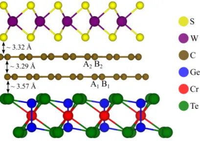
and stretch the lattice constant of CGT by roughly 6% to 7.2169 ˚A [2]. The WS2 lattice constant is compressed by about 1% to 3.125 ˚A [3]. The supercell of WS2/BLG/CGT has a lattice constant of 12.5 ˚A and contains 178 atoms in the unit cell. In Fig. S1 we show the exact geometry, akin to Fig. 1 of the main text, including relaxed interlayer distances of the CGT/BLG/WS2hybrid structure. The obtained interlayer distances are similar as reported in Refs.
[4, 5]. The lower (upper) graphene layer, formed by sublattices A1 and B1 (A2 and B2), is proximitized by the CGT (WS2) only, due to the short range proximity effect.
FIRST-PRINCIPLES CALCULATIONS
The electronic structure calculations and structural relaxation of the BLG-based heterostructures are performed by DFT [6] withQuantum ESPRESSO [7]. Self-consistent calculations are performed with the k-point sampling of 12×12×1 to get converged results for the proximity exchange and spin-orbit coupling. For the CGT/BLG/WS2
heterostructure, when spin-orbit coupling is included, a smallerk-point sampling of 6×6×1 is used. We perform open shell calculations that provide the spin polarized ground state of CGT. A Hubbard parameter ofU = 1 eV is used for Crd-orbitals, being in the range of proposed values for CGT [5, 8]. We use an energy cutoff for charge density of 500 Ry, and the kinetic energy cutoff for wavefunctions is 60 Ry for the scalar relativistic pseudopotential with the projector augmented wave method [9] with the Perdew-Burke-Ernzerhof exchange correlation functional [10]. When SOC is included, we use the relativistic versions of the pseudopotentials. For the relaxation of the heterostructures, we add van der Waals corrections [11, 12] and use quasi-newton algorithm based on trust radius procedure. Dipole corrections [13] are also included to get correct band offsets and internal electric fields. In order to simulate quasi-2D systems, we add a vacuum of 20 ˚A, to avoid interactions between periodic images in our slab geometry. To determine the interlayer distances, the atoms of BLG and WS2 are allowed to relax only in their z positions (vertical to the layers), and the atoms of CGT are allowed to move in all directions, until all components of all forces are reduced below 10−3 [Ry/a0], wherea0is the Bohr radius.
HETEROSTRUCTURE OF BLG, CGT, AND WS2
Here we present the Hamiltonian used to model the doubly proximitized BLG. The basis states are|CA1,↑i,|CA1,↓i,
|CB1,↑i, |CB1,↓i,|CA2,↑i,|CA2,↓i, |CB2,↑i, and|CB2,↓i. In this basis the Hamiltonian from the main text is (see also Ref. 14)
H=Horb+Hsoc+Hex+HR+ED, (S1)
Horb =
∆ +V γ0f(k) γ4f∗(k) γ1
γ0f∗(k) V γ3f(k) γ4f∗(k) γ4f(k) γ3f∗(k) −V γ0f(k)
γ1 γ4f(k) γ0f∗(k) ∆−V
⊗s0, (S2)
Hsoc+Hex+HR=
(τ λA1I −λA1ex)sz i(λ0+ 2λR)sτ− 0 0
−i(λ0+ 2λR)sτ+ (−τ λB1I −λB1ex)sz 0 0 0 0 (τ λA2I −λA2ex)sz −i(λ0−2λR)sτ− 0 0 i(λ0−2λR)sτ+ (−τ λB2I −λB2ex)sz
. (S3)
We use the linearized version for the nearest-neighbor structural functionf(k) =−√23a(τ kx−iky) and introduce also sτ±= 12(sx±iτ sy) for shorter notation.
TABLE S1. Fit parameters of the model HamiltonianH, Eq. (1) in the main text, for the BLG/WS2structure with SOC, for the CGT/BLG structure without SOC, and for the CGT/BLG/WS2structure without SOC. Unspecified parameters are zero.
system BLG/WS2 (SOC) CGT/BLG (no SOC) CGT/BLG/WS2 (no SOC)
γ0 [eV] 2.453 2.541 2.434
γ1 [eV] 0.372 0.384 0.365
γ3 [eV] -0.270 -0.296 -0.269
γ4 [eV] -0.162 -0.179 -0.165
V [meV] 4.226 -8.499 -0.479
∆ [meV] 10.208 10.434 8.649
λA2I [meV] 1.070 0 0
λB2I [meV] -1.179 0 0
λA1ex [meV] 0 -4.567 -4.257
λB1ex [meV] 0 -4.224 -3.997
ED [meV] -3.844 -1.003 -0.336
dipole [debye] -1.089 1.527 0.366
In Fig. S1, we present a side view of the CGT/BLG/WS2heterostructure. The interlayer distance are of typical van der Waals type and similar as obtained in Refs. [4, 5]. In Tab. S1, we summarize the fit results for the CGT/BLG/WS2
stack, when spin-orbit coupling (SOC) is not included in the calculation. The results are similar to the case with SOC, as listed in Tab. (1) in the main text, but SOC parameters are zero.
In Fig. S2 (Fig. S3), we show the calculated low energy bands with the model fit for zero (finite) electric field. Figs.
S2 and S3 are more detailed views of the DFT-fitted bands, as shown in Fig. (3) from the main text. In all cases, the model agrees very well with the first-principles data and also band splittings are well reproduced. As described in the main text, we use the DFT-fitted parameters for zero electric field from Tab. (1) and tuneV to match the finite electric field cases. An animation (Efield movie.mp4) showing the evolution of the low energy bands of doubly proximitized BLG atK andK0, for a series of electric fields is also available.
3
FIG. S1. Side view of the CGT/BLG/WS2heterostructure. Different colored spheres correspond to the different atomic species.
The lower (upper) graphene layer of BLG is formed by sublattices A1 and B1 (A2 and B2). The relaxed interlayer distances are also indicated.
−20
−10 0 10 20 30
M ← K → Γ
2 1 0 1 2
E − EF[meV]
k [10−2/Å]
ModelDFT
−0.5 0 0.5
< sz>
2 4 6
M ← K → Γ
2 1 0 1 2
splitting [meV]
k [10−2/Å]
∆ECB
∆EVB
−0.5 0 0.5
M ← K’ → Γ
2 1 0 1 2
VB1
k [10−2/Å]
−0.5 0 0.5
M ← K’ → Γ
2 1 0 1 2
VB2
k [10−2/Å]
−0.5 0 0.5
M ← K’ → Γ
2 1 0 1 2
CB1
k [10−2/Å]
−0.5 0 0.5
M ← K’ → Γ
2 1 0 1 2
CB2
k [10−2/Å]
sx sy sz
−20
−10 0 10 20 30
M ← K’ → Γ
2 1 0 1 2
E − EF[meV]
k [10−2/Å]
2 4 6
M ← K’ → Γ
2 1 0 1 2
splitting [meV]
k [10−2/Å]
(a)
(b)
(c)
(d)
FIG. S2. (a) Zoom to the calculated low energy bands (symbols) around theKpoint with a fit to the model Hamiltonian (solid lines) for the WS2/BLG/CGT heterostructure including SOC for zero electric field. (b) Energy splittings of the conduction and valence band. (c,d) Same as (a,b), but for theK0 point.
−30
−20
−10 0 10 20 30
M ← K → Γ
2 1 0 1 2
E − E
F[meV]
k [10
−2/Å]
−0.5 0 0.5
< s
z>
−30
−20
−10 0 10 20 30
M ← K’ → Γ
2 1 0 1 2
E − E
F[meV]
k [10
−2/Å]
−0.5 0 0.5
< s
z>
−30
−20
−10 0 10 20 30
M ← K → Γ
2 1 0 1 2
E − E
F[meV]
k [10
−2/Å]
Model DFT
−0.5 0 0.5
< s
z>
−30
−20
−10 0 10 20 30
M ← K’ → Γ
2 1 0 1 2
E − E
F[meV]
k [10
−2/Å]
−0.5 0 0.5
< s
z>
(a) (b)
(c) (d)
FIG. S3. Calculated (symbols) low energy band structures with a fit to the model Hamiltonian (solid lines), aroundKandK0 points for WS2/BLG/CGT heterostructure including SOC. (a,b) For transverse electric field of +0.4 V/nm and a calculated dipole of 2.755 Debye. (c,d) For transverse electric field of−0.5 V/nm and a calculated dipole of -2.649 Debye.
5 HETEROSTRUCTURE OF BLG AND WS2
For the WS2/BLG heterostructure, we choose a 5×5 supercell of BLG in Bernal stacking and a 4×4 supercell of WS2. We stretch the lattice constant of graphene by roughly 2% to 2.5 ˚A and the WS2lattice constant is compressed by about 1% from 3.153 ˚A [3] to 3.125 ˚A. The supercell of WS2on BLG has a lattice constant of 12.5 ˚A and contains 148 atoms in the unit cell.
FIG. S4. (a,b) Band structure with SOC and geometry of WS2on BLG. (c) Zoom to the calculated low energy bands (symbols) around theK point with a fit to the model Hamiltonian (solid lines). The color corresponds to thesz expectation value. (d) Energy splittings of the conduction and valence band.
Recent first-principles calculations have shown that for BLG on WS2, there exists a spin-valve effect [4]. In Figs.
S4(a,b) we show the band structure and a side view of the geometry of WS2 on BLG. The results are in perfect agreement with Ref. [4]. We go one step further and fit our BLG low energy model Hamiltonian from the main text to the DFT calculated bands and find perfect agreement between the model and the ab-initio data, see Figs.
S4(c,d). The fit parameters are summarized in Tab. S1 for the BLG/WS2 heterostructure. The low energy valence band originates from the top graphene layer formed by sublattices A2 and B2. Because of the short range nature of proximity SOC, only this top layer is proximitized by the WS2. Therefore the valence band experiences strong SOC induced spin splitting, while the conduction band splitting is much smaller near theKpoint.
Because of this short rangeness of proximity SOC and the unique BLG band structure, the splitting can be switched from the valence band to the conduction band by applying a transverse electric field across the heterostructure [4, 15], and spin relaxation of electrons and holes can be controlled fully electrically.
HETEROSTRUCTURE OF BLG AND CGT
For the BLG/CGT heterostructure, we choose a 5×5 supercell of BLG in Bernal stacking and a √ 3×√
3 CGT supercell. We keep the lattice constant of graphene unchanged ata= 2.46 ˚A and stretch the CGT lattice constant by roughly 4% from 6.8275 ˚A [2] to 7.1014 ˚A. The supercell of BLG on CGT has a lattice constant of 12.3 ˚A and contains 130 atoms in the unit cell.
Similar to before, in Figs. S5(a,b) we show the band structure and a side view of the geometry of BLG on CGT.
In this case, the bottom graphene layer formed by sublattices A1and B1 experiences strong proximity exchange from CGT. This system has recently been considered in Ref. [5], where an exchange valve effect has been found. Again, we fit our low energy model to the first-principles data and find perfect agreement, see Figs. S5(c,d). Here, the valence band, which originates from the bottom graphene layer formed by sublattices A1and B1, is strongly split due to proximity exchange. In contrast, the conduction band splitting is negligible, again due to short rangeness of the proximity effect. The fit parameters are also summarized in Tab. S1 for the CGT/BLG heterostructure.
FIG. S5. (a,b) Band structure without SOC and geometry of BLG on CGT. (c) Zoom to the calculated low energy bands (symbols) around theK point with a fit to the model Hamiltonian (solid lines). Bands in red (blue) correspond to spin up (down). (d) Energy splittings of the conduction and valence band.
∗ klaus.zollner@physik.uni-regensburg.de
[1] Baskin, Y. & Meyer, L. Lattice Constants of Graphite at Low Temperatures. Phys. Rev.100, 544 (1955).
7 [2] Carteaux, V., Brunet, D., Ouvrard, G. & Andre, G. Crystallographic, magnetic and electronic structures of a new layered
ferromagnetic compound Cr2Ge2Te6. J. Phys.: Condens. Mat.7, 69 (1995).
[3] Schutte, W. J., De Boer, J. L. & Jellinek, F. Crystal structures of tungsten disulfide and diselenide.J. Solid State Chem.
70, 207 (1987).
[4] Gmitra, M. & Fabian, J. Proximity Effects in Bilayer Graphene on Monolayer WSe2: Field-Effect Spin Valley Locking, Spin-Orbit Valve, and Spin Transistor. Phys. Rev. Lett.119, 146401 (2017).
[5] Zollner, K., Gmitra, M. & Fabian, J. Electrically tunable exchange splitting in bilayer graphene on monolayer Cr2X2Te6
with X = Ge, Si, and Sn. New J. Phys.20, 073007 (2018).
[6] Hohenberg, P. & Kohn, W. Inhomogeneous Electron Gas.Phys. Rev.136, B864 (1964).
[7] Giannozzi, P.et al. QUANTUM ESPRESSO: a modular and open-source software project for quantum simulations of materials. J. Phys.: Cond. Mat.21, 395502 (2009).
[8] Gong, C.et al. Discovery of intrinsic ferromagnetism in two-dimensional van der Waals crystals.Nature 546, 265 (2017).
[9] Kresse, G. & Joubert, D. From ultrasoft pseudopotentials to the projector augmented-wave method. Phys. Rev. B 59, 1758 (1999).
[10] Perdew, J. P., Burke, K. & Ernzerhof, M. Generalized Gradient Approximation Made Simple. Phys. Rev. Lett.77, 3865 (1996).
[11] Grimme, S. Semiempirical GGA-type density functional constructed with a long-range dispersion correction. J. Comput.
Chem.27, 1787 (2006).
[12] Barone, V.et al. Role and effective treatment of dispersive forces in materials: Polyethylene and graphite crystals as test cases. J. Comput. Chem.30, 934 (2009).
[13] Bengtsson, L. Dipole correction for surface supercell calculations. Phys. Rev. B 59, 12301 (1999).
[14] Konschuh, S., Gmitra, M., Kochan, D. & Fabian, J. Theory of spin-orbit coupling in bilayer graphene. Phys. Rev. B 85, 115423 (2012).
[15] Island, J. O.et al. Spin-orbit-driven band inversion in bilayer graphene by the van der Waals proximity effect. Nature 571, 85 (2019).