Editors’ Suggestion
Proximity exchange effects in MoSe 2 and WSe 2 heterostructures with CrI 3 : Twist angle, layer, and gate dependence
Klaus Zollner ,
*Paulo E. Faria Junior, and Jaroslav Fabian
Institute for Theoretical Physics, University of Regensburg, 93040 Regensburg, Germany
(Received 24 June 2019; revised manuscript received 1 August 2019; published 16 August 2019) Proximity effects in two-dimensional (2D) van der Waals heterostructures offer controllable ways to tailor the electronic band structure of adjacent materials. Proximity exchange in particular is important for making materi- als magnetic without hosting magnetic ions. Such synthetic magnets could be used for studying magnetotransport in high-mobility 2D materials, or magneto-optics in highly absorptive nominally nonmagnetic semiconductors.
Using first-principles calculations, we show that the proximity exchange in monolayer MoSe
2and WSe
2due to ferromagnetic monolayer CrI
3can be tuned (even qualitatively) by twisting and gating. Remarkably, the proximity exchange remains the same when using antiferromagnetic CrI
3bilayer, paving the way for optical and electrical detection of layered antiferromagnets. Interestingly, the proximity exchange is opposite to the exchange of the adjacent antiferromagnetic layer. Finally, we show that the proximity exchange is confined to the layer adjacent to CrI
3, and that adding a separating hBN barrier drastically reduces the proximity effect. We complement our ab initio results with tight-binding modeling and solve the Bethe-Salpeter equation to provide experimentally verifiable optical signatures (in the exciton spectra) of the proximity exchange effects.
DOI: 10.1103/PhysRevB.100.085128
I. INTRODUCTION
Two-dimensional (2D) materials and their hybrids offer unforeseen opportunities, but also challenges, to electronics, spintronics, optics and magnetism [1–5]. Graphene, the pro- totypical 2D crystal, has excellent charge and spin transport properties [6–9], but lacks an orbital band gap needed for digital transistor applications. Fortunately, we have now avail- able a large class of air-stable 2D semiconductors—transition- metal dichalcogenides (TMDCs)—which have a band gap in the optical range [10–14], and form a favorite platform for optical experiments including optical spin injection due to helicity-selective optical exitations [15]: electrons in opposite valleys, but at the same energy, feel opposite spin-orbit fields, pointing out of the plane. This effect is called valley Zeeman coupling; unlike true Zeeman field, the valley coupling pre- serves time reversal symmetry, since it stems from spin-orbit coupling (SOC).
In fact, one can create a proximity structure from graphene and a TMDC, initially proposed by DFT calculations [16]
and confirmed experimentally [17,18] to facilitate transfer of the optically generated spin in TMDC into graphene. This is an example of a proximity effect [19] in van der Waals het- erostructures. Proximity effects provide fascinating opportu- nities for band-structure engineering. Experiments and theory show that graphene can borrow different properties from a variety of substrates, be it SOC or magnetism [16,20–26].
For all-2D spintronics, it is desirable to integrate 2D materials such as graphene and TMDCs with 2D magnets.
Experimentalists have demonstrated magnetic order in 2D layered crystals, such as MnSe
2[27,28], CrGeTe
3[29–34],
*
klaus.zollner@physik.uni-regensburg.de
and CrI
3[35–44], which are well suited for nanoelectronic devices [45]. Unlike thin films of conventional ferromagnets, which have magnetization typically in the plane (of the film), the 2D layered ferromagnets have magnetization pointing out of the plane, making them Ising-like.
This out-of-plane exchange interaction is a time-reversal breaking analog of the valley Zeeman splitting in TMDCs.
The interplay of the two couplings, exchange and valley Zeeman, motivates explorations of stacked TMDCs and 2D ferromagnets. Certainly, one can introduce Zeeman coupling by applying an external magnetic field pointing out of the plane, but such fields produce modest valley splittings, about 0.1–0.2 meV per tesla [46–49]. Proximity exchange fields can induce much stronger effects, perhaps up to hundreds of meVs, without significantly altering the band structure of TMDCs [50–62]. Conventional ferromagnetic substrates, such as EuO or MnO, were predicted to give 200–300 meV [57–59]; experiments on EuS find only 2.5 meV [60], pre- sumably due to uneven interfaces.
There already are experiments demonstrating proximity exchange in TMDCs. Recent measurements in TMDC/CrI
3heterostructures [54,61] show a few meV of proximity ex-
change. CrI
3is especially interesting, because the monolayer
is a ferromagnet (FM) [39,63], while bilayer CrI
3shows an-
tiferromagnetic (AFM) coupling [39,64,65], in contradiction
to the existing theory [41,63,66] which predicts a FM state
for the low temperature phase. Remarkably, the magnetization
of the CrI
3can be tuned optically [61], thereby influencing
proximity exchange and the photoluminescence (PL) spec-
trum of the TMDC. In addition, the magnetism in few layer
CrI
3can be controlled by gating and external magnetic fields
[42,43], opening a new path for gate controlled devices, such
as spin-filter tunnel junctions [65,67,68], and AFM spintron-
ics [69,70].
ZOLLNER, FARIA JUNIOR, AND FABIAN PHYSICAL REVIEW B 100, 085128 (2019) Here, we provide a systematic theoretical analysis of the
proximity exchange coupling in TMDC / CrI
3heterostructures (with MoSe
2and WSe
2as TMDC) from first-principles.
First, we confirm that the magnetic insulator substrate couples weakly to the TMDC by van der Waals forces, preserving the characteristic electronic band structure of the TMDC.
The proximity exchange coupling splits the conduction (CB) and valence band (VB) of the TMDC by roughly 1–5 meV, and combined with the intrinsic (valley Zeeman) SOC of the TMDC lifts the valley degeneracy. We introduce a min- imal model Hamiltonian to describe the proximity effects in TMDC due to CrI
3, extracting realistic proximity exchange parameters which should be useful for modeling transport and optics.
Next, and this is the main result of the paper, we find wide tunability of proximity exchange effects with respect of twisting and gating, and the absence of effects coming from additional layers (both TMDC and CrI
3). In particular, we find that proximity exchange splittings depend on the twist angle between the TMDC and the CrI
3. We investigated 0
◦and 30
◦structures, and observed that not only the magnitudes of the exchange differ, but, remarkably, the direction of the exchange field for holes changes sign. The exchange parameters can be tuned by a few meVs by gating, using accessible electric fields of a few V/nm.
It is rather fascinating that adding another layer of CrI
3does not affect the proximity exchange in TMDCs (we used MoSe
2), given that the two magnetic layers are antiferromag- netically coupled and they have zero net magnetic moment.
The proximity effect can then be used to detect, optically or electrically, the magnetic moment of the adjacent (to the TMDC) CrI
3layer even in the antiferromagnetic state. We also explicitly prove the short-range nature of the proximity effects by investigating bilayer-MoSe
2/CrI
3and MoSe
2/hBN/CrI
3. In the former, the proximity affects the adjacent TMDC layer, while in the latter the insulating hBN layer drastically reduces the proximity exchange. This message is important since experimentally it may be desirable to cover CrI
3with hBN first, to improve its stability under ambient conditions. For proximity effects, using hBN barriers would be detrimental.
Finally, we give specific predictions for optical signatures of the proximity exchange effects, by calculating the excitonic absorption spectra employing the Bethe-Salpeter equation.
The twist-angle and gate-bias dependence of the proximity exchange is mapped into the valley splitting of the first intralayer exciton peak. This is a valuable and experimentally testable fingerprint of our results.
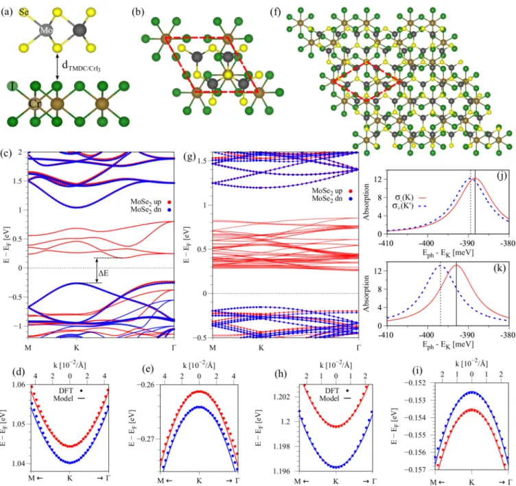
II. BAND STRUCTURE, GEOMETRY, AND TWIST EFFECTS
To study proximity exchange effects, we set up a common unit cell for the TMDC/CrI
3heterostructures (see Ref. [71]).
We consider a 2 × 2 supercell for the TMDCs (MoSe
2and WSe
2) above a 1 × 1 cell of CrI
3, as well as a larger 7 × 7 supercell of the TMDC on top of a (2 √
3 × 2 √
3)R30
◦super- cell of CrI
3. In Figs. 1(a) and 1(b), we show the geometry of the MoSe
2/CrI
3heterostructure, as a typical structure of the small supercell with 0
◦twist angle. In Fig. 1(f), we show
the top view of the larger supercell which is twisted by 30
◦relative to the underlying CrI
3.
In Figs. 1(c)–1(e), we show the calculated band structure with a fit to our model Hamiltonian (see Ref. [71]) for the small MoSe
2/CrI
3supercell structure without SOC (to extract the exchange coupling). We find that the bands of the TMDC are nicely preserved but are marked with a proximity exchange. The spin up CBs, originating from the CrI
3, are located within the band gap of the TMDC, see Fig. 1(c).
In experiments it was already shown that the spin polarized in-gap states from the CrI
3quench the PL spectrum for one light helicity only [54,61], due to additional nonradiative relaxation processes. The energy gap of the full heterostruc- ture is E ≈ 400 meV, as defined in Fig. 1(c). The band edges of the TMDC can be almost perfectly described by our model Hamiltonian, as shown in Figs. 1(d) and 1(e). Due to proximity exchange, the bands are spin split by about 5 meV.
In Figs. 1(g)–1(i), we present the calculated band structure with a fit to our model Hamiltonian for the larger MoSe
2/ CrI
3supercell structure with 30
◦twist angle without SOC. As there are much more atoms in the supercell, more in-gap states from the CrI
3are located within the band gap of the TMDC.
The proximity exchange is clearly visible. In comparison to the smaller, 0
◦supercell, the VB splitting is opposite in sign.
Unfortunately, studying other, especially small twist angles is beyond our DFT approach. However, the different direction of the exchange field in VB seen for 0
◦and 30
◦structures shows that twisting can be an effective tool to modify the proximity effect. Similar effect was predicted in SOC proximity effect, by placing graphene on a topological insulator. Two different twist angles produced qualitatively different spin-orbit fields in graphene [72].
To investigate the optical signatures of the proximity ex- change due to the twist angle, we calculate the absorption spectra of the intralayer excitons, i.e., electron-hole pairs created directly at the TMDC layer that are experimentally accessible in PL spectra [54,61]. For these calculations, we apply the effective Bethe-Salpeter equation [73–76] using the model Hamiltonian fitted to the first-principles band structure, see Figs. 1(d), 1(e), 1(h), and 1(i). For these calculations, we also consider the effects of SOC by combining the parame- ters summarized in Table I (see Ref. [71] for details of the excitonic calculations and the model Hamiltonian). Focusing on the lowest energy excitonic levels, we show in Figs. 1(j) and 1(k) the first absorption peak at K ( σ
−polarization) and K
( σ
+polarization) valleys for 0
◦and 30
◦twist angles. We find that the valley splitting (the energy separation between the two absorption peaks) shows a substantial threefold increase by changing the twist angle, from ∼1.13 meV for 0
◦to
∼3.89 meV for 30
◦. Interestingly, these energy splittings
calculated within the single-particle picture ( ∼ 1 . 25 meV for
0
◦and ∼4.29 meV for 30
◦) are in reasonable agreement
with the excitonic calculations. We also performed a similar
investigation for WSe
2/CrI
3heterostructures and found an ex-
citonic (single-particle) valley splitting of ∼1.43 (1.61) meV
for 0
◦and ∼ 6 . 35 (7.09) meV for 30
◦, thus providing a
dramatic ∼ 4 . 4-fold increase due to twist angle. In recent
experiments by Zhong et al. [54], the measured valley splitting
in WSe
2/CrI
3is ∼3.5 meV (equivalent to ∼13 T external
magnetic field in bare WSe
2), and thus it is reasonable to
FIG. 1. Calculated band structures without SOC, geometries, and absorption spectra of MoSe
2/ CrI
3. [(a) and (b)] Side and top view of the small supercell geometry (0
◦twist angle) with labels for the different atoms and the definition of the interlayer distance d
TMDC/CrI3. One unit cell of CrI
3is highlighted, by the red dashed line, in the top view. (c) Band structure along high-symmetry lines, with the energy gap of the heterostructure E. The bands corresponding to MoSe
2are emphasized by red (spin up) and blue (spin down) spheres. [(d) and (e)] Zoom to the CB and VB edge corresponding to MoSe
2. Symbols are DFT data and solid lines are the fitted model Hamiltonian. [(f)–(i)] The top view, calculated band structure, and the zoom to the low-energy bands for the larger supercell geometry (30
◦twist angle). [(j) and (k)] Calculated first absorption peak of intralayer excitons for small (b) and large (f) geometry (including SOC) with the vertical solid (dashed) arrows indicating the peak position for the absorption at K (K
) point.
expect that the structure (or part of it, depending on the qual- ity) was twisted. Undoubtedly, the WSe
2/CrI
3heterostructure demands further experimental investigations of proximity ex- change, especially with respect to different values of the twist angle. A similar twist angle dependence of proximity SOC has been reported for graphene/TMDC heterostructures [77].
As a magnetic field or proximity exchange breaks time- reversal symmetry, we show the calculated band structure
for MoSe
2/CrI
3with SOC in Fig. 2, for the 0
◦twist angle supercell. We find a very good agreement between the model Hamiltonian and the calculated bands around K and K
valley.
The valley degeneracy is now broken, especially when com- paring the CB edges at K and K
valley, see Figs. 2(b) and 2(c).
Therefore a TMDC/CrI
3heterostructure shows valley polar-
ization of the TMDC, in agreement with recent measurements
[54,61], and other first-principles calculations [78]. Inclusion
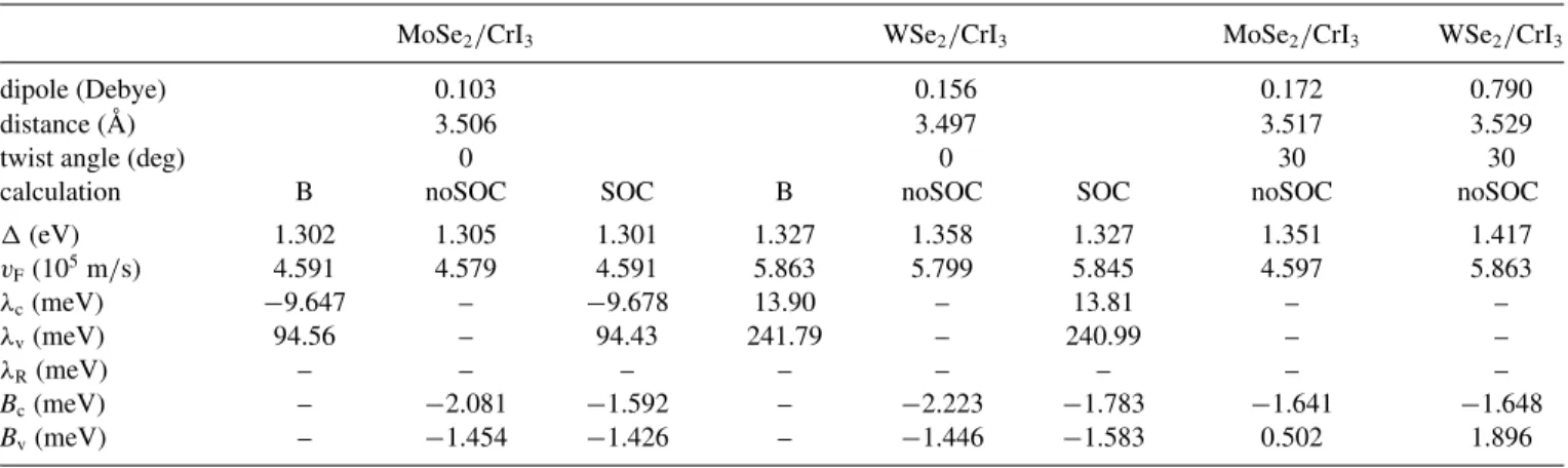
ZOLLNER, FARIA JUNIOR, AND FABIAN PHYSICAL REVIEW B 100, 085128 (2019) TABLE I. Summary of fit parameters, calculated dipoles and distances for TMDC/CrI
3systems. The orbital gap of the spectrum and the Fermi velocity v
F. The parameters λ
cand λ
vdescribe the SOC splittings, and B
cand B
vare the proximity exchange parameters for CB and VB. The dipole of the structures is given in debye and the distance d
TMDC/CrI3is defined in Fig. 1(a). The twist angle 0
◦(30
◦) corresponds to the small (large) supercell in Fig. 1. The individual columns are for calculations of the bare TMDC (B) with the modified lattice constant from the heterostructure, the heterostructure without SOC (noSOC) and with SOC.
MoSe
2/CrI
3WSe
2/CrI
3MoSe
2/CrI
3WSe
2/CrI
3dipole (Debye) 0.103 0.156 0.172 0.790
distance (Å) 3.506 3.497 3.517 3.529
twist angle (deg) 0 0 30 30
calculation B noSOC SOC B noSOC SOC noSOC noSOC
(eV) 1.302 1.305 1.301 1.327 1.358 1.327 1.351 1.417
v
F(10
5m/s) 4.591 4.579 4.591 5.863 5.799 5.845 4.597 5.863
λ
c(meV) − 9.647 – − 9.678 13.90 – 13.81 – –
λ
v(meV) 94.56 – 94.43 241.79 – 240.99 – –
λ
R(meV) – – – – – – – –
B
c(meV) – − 2.081 − 1.592 – − 2.223 − 1.783 − 1.641 − 1.648
B
v(meV) – −1.454 −1.426 – −1.446 −1.583 0.502 1.896
of SOC effects for the large supercell structure is beyond our computational possibilities and therefore not included here.
In order to qualitatively extract, the influence from the FM substrate, we calculate the band structure of the TMDC / CrI
3heterostructures, for MoSe
2and WSe
2in the small supercell
FIG. 2. Calculated band structure of MoSe
2/ CrI
3with SOC for the 0
◦twist angle structure. (a) Band structure along high-symmetry lines. Color corresponds to the s
z-expectation value. (b,c) Zoom to the CB edge corresponding to MoSe
2at K and K
. Symbols are DFT data and solid lines are the fitted model Hamiltonian. [(d) and (e)]
Same as (b) and (c) but for VB edge.
geometry, and fit it to our low-energy Hamiltonian [71]. To obtain reasonable fit parameters, we consider three situations.
First, we calculate the band structure for the bare TMDC, removing the CrI
3, and check the SOC parameters for this situation, with the modified lattice constant used in the het- erostructure geometry. This is crucial, because an increase in the lattice constant diminishes, for example, the band gap of the TMDC [79–82]. Second, we calculate the band structure for the TMDC / CrI
3heterostructures without SOC in order to obtain the proximity exchange splitting parameters.
Finally, we calculate the band structure for the TMDC/CrI
3heterostructures with SOC. In Table I, we summarize the fit results for the three mentioned calculations, for 0
◦twist angle.
Additionally, we give the fit results for the 30
◦twist angle case, corresponding to Figs. 1(f)–1(i) without SOC.
Especially interesting are the proximity exchange param- eters, being roughly 2 meV in magnitude, translating into about 10 T exchange field [46–49], in agreement with recent experiments [54,61]. The calculation of the atomic magnetic moments reveals, that the magnetization direction of the TMDC is the same as in the I atoms, opposite to the Cr atoms, therefore giving negative proximity exchange parameters for a net CrI
3magnetization pointing along positive z direction towards the TMDC. As there are many atoms in the unit cells, we calculate averaged magnetic moments for the different atomic species. The averaged magnetic moments for the small nontwisted supercell are Cr (+3.53 μ
B), I (−0.19 μ
B), Mo (−0.0039 μ
B), and Se (−0.0046 μ
B). We averaged only over Se atoms closer to the CrI
3substrate, as they mediate the proximity exchange to the Mo atoms. The averaged magnetic moments for the large twisted supercell are Cr ( + 3 . 46 μ
B), I (−0.18 μ
B), Mo (−0.0029 μ
B), and Se (−0.0031 μ
B).
Including SOC in the heterostructure calculations, we find
the parameters to be barely different than those from the
individual calculations for the bare TMDCs or for the het-
erostructures without SOC. Therefore, combining the model
Hamiltonian, the SOC parameters from the bare TMDC
monolayer, and the exchange parameters from the heterostruc-
ture calculation without SOC, already suffices to get a
reasonable low-energy band structure. Our fit shows that the
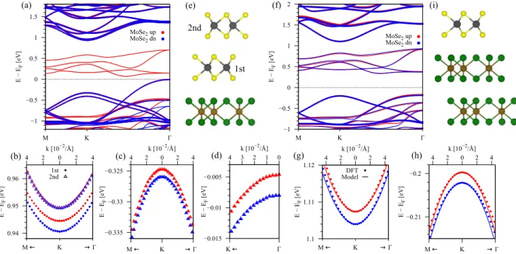
FIG. 3. (a) Band structure along high-symmetry lines for bilayer MoSe
2on top of monolayer CrI
3. In (a)–(h), spin up (down) bands are plotted in red (blue), while symbols emphasize the character of the bands. In (a), the bands corresponding to bilayer MoSe
2are emphasized by thicker spheres. (b) Zoom to the CB edge around the K point. [(c) and (d)] Same as (b), but for VB edge around K and point. In (b)–(d), the bands corresponding to the first (second) layer of the bilayer MoSe
2are emphasized by filled spheres (open triangles). (e) Side view of the geometry with definition of first and second layer of 2H bilayer MoSe
2. (f) Band structure along high-symmetry lines for monolayer MoSe
2on top of bilayer CrI
3in the AFM (↑↓) configuration. (g) Zoom to the CB edge around the K point (symbols), with a fit to the model Hamiltonian (solid line). (h) Same as (g), but for VB edge. (i) Side view of the geometry of monolayer MoSe
2on bilayer CrI
3.
Rashba parameter is not necessary to capture the essentials of the band structure for the TMDC/CrI
3stacks, because there is no in-plane component of the spin expectation value present around the band edges.
From the experimental point of view, when materials are mechanically exfoliated and stacked, one can expect various local interface (stacking) configurations between the TMDC and CrI
3, different to what is shown in Fig. 1(b). However, our calculations show that proximity exchange splittings are marginally affected by different interface configurations, see Ref. [71].
III. SHORT-RANGENESS OF PROXIMITY EFFECTS A. Bilayer TMDC on monolayer CrI
3In experiment, when the TMDC is exfoliated from bulk crystals, it may also happen that a bilayer TMDC is transferred onto the magnetic CrI
3substrate. Does the second TMDC layer also experience proximity exchange, or only the closest layer? To answer this question, we consider 2H bilayer MoSe
2on top of monolayer CrI
3. We first allow for relaxation of the whole geometry, similar to the monolayer MoSe
2case, to get reasonable interlayer distances.
In Fig. 3(a), we show the calculated band structure of 2H bilayer MoSe
2on top of monolayer CrI
3without consider- ing SOC effects. The bilayer TMDC has an indirect band gap, consistent with literature [83,84]. For the CB edge, see Fig. 3(b), we can identify the bands originating from the first and second layer of the bilayer MoSe
2. The bands from the first layer are spin-split, similar to what we observe for the
monolayer MoSe
2case, while the bands originating from the second layer experience negligible splitting. The VB edge around the K point, see Fig. 3(c), is formed by two nonde- generate bands, a spin up and a spin down one, which are split in energy. The magnitude of the splitting is again similar to the monolayer case and a result of proximity exchange. However, we find that each band is formed by orbitals from both TMDC layers, which does not allow us to trace back the splitting to proximity exchange in a specific layer. For further insights, we show the calculated layer- and spin-resolved density of states, see Ref. [71]. In additon, the calculated magnetic moments for the second layer (−0.0001 μ
B) are much smaller than for the first layer (−0.004 μ
B). Thus we conclude that the proximity exchange is mainly induced in the TMDC layer closest to the CrI
3substrate.
B. TMDC on antiferromagnetic bilayer CrI
3Another feature which was especially observed in bilayer CrI
3is the switching from FM to AFM coupled layers by gating [39,42]. For the AFM state, there are two energetically degenerate states of the bilayer (first layer ↑, second layer
↓, or vice versa). Therefore we calculate the band structure,
with and without SOC, for MoSe
2on top of bilayer CrI
3,
which is stacked in the low temperature rhombohedral phase
[41,63,66]. We find a total energy difference of E
AFM−
E
FM≈ 24 meV between the FM and the AFM state calculated
without SOC of the whole TMDC/bilayer-CrI
3stack, which
contains four Cr atoms in our supercell. In agreement with
previous DFT calculations [41,63,66], we find that the FM
ZOLLNER, FARIA JUNIOR, AND FABIAN PHYSICAL REVIEW B 100, 085128 (2019) state of the bilayer CrI
3is energetically favorable compared
to the AFM state in contrast to experiments [39,64,65].
In Fig. 3(f), we show the calculated band structure of MoSe
2on top of bilayer CrI
3without SOC, when the bilayer CrI
3is in the AFM (↑↓) configuration (the magnetization of the CrI
3layer directly below the TMDC is pointing ↑).
In Ref. [71], we show the band structures including SOC for both cases, the FM and AFM configuration. The fit to the low-energy bands, see Figs. 3(g) and 3(h) are similar to what is shown in Fig. 1 for MoSe
2on top of monolayer CrI
3. The naive expectation is that, depending on the total magnetization of the bilayer CrI
3, we can enhance or reduce proximity exchange in the TMDC, compared to the monolayer CrI
3case. However, we find that the FM (↑↑) or AFM (↑↓) coupled bilayer give almost no difference in the fit parameters compared to the monolayer case [71].
C. Effects of hBN barrier
Finally, when introducing a hBN buffer layer be- tween the MoSe
2and CrI
3, proximity exchange split- tings of the MoSe
2bands are drastically reduced to about 100 μeV [71]. The calculated averaged magnetic moments for the case of MoSe
2/hBN/CrI
3are Cr (+3.50 μ
B), I (−0.19 μ
B), N (−0.0016 μ
B), B (0.0 μ
B), Mo (−0.0001 μ
B), and Se (−0.0001 μ
B). The magnetic moments in the TMDC are reduced by one order of magnitude, compared to the case without the hBN layer. By looking at the proximity exchange in the hBN layer, we find that the bands originating from hBN are strongly hybridized with the CrI
3bands, see Ref. [71].
This can be helpful for interpreting tunneling experiments of such heterostructures. All these results indicate that proximity exchange is truly a short range effect, and can be used to create and detect the magnetic order in the layered AFM, bilayer CrI
3[71].
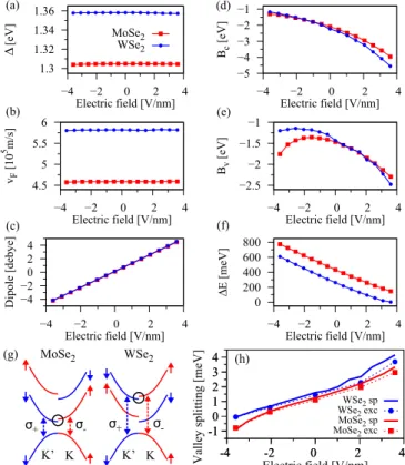
IV. GATE TUNABLE PROXIMITY EXCHANGE AND EXCITON SPLITTING
Motivated by recent experiments [39,42,43], showing the electric field control of magnetism in few layer CrI
3, and the optical tuning of proximity exchange in TMDC/CrI
3heterostructures [61], we perform additional calculations for our heterostructures, where we apply a transverse electric field across the geometry consisting of one monolayer of TMDC and one of CrI
3.
As calculations without SOC already give reasonable prox- imity exchange parameters, we neglect SOC for the electric field study. In Fig. 4, we show the fit parameters as a function of a transverse electric field for TMDC/CrI
3heterostructures calculated without SOC, for the 0
◦twist angle structures. We find that the gap parameter , as well as the Fermi velocity v
Fare barely affected by external electric fields. The dipole of the heterostructure depends linearly on the electric field.
By applying an electric field, the band offsets can be changed.
The band gap E of the heterostructure, defined in Fig. 1(c), shrinks linearly with applied electric field. This tunability of the band offsets could be very important for other effects.
Imagine electrons located in the CrI
3layer coupled to holes in the TMDC layer. As we apply an electric field, we tune
(a) (d)
(b) (e)
(c) (f)
1.3 1.32 1.34 1.36
−4 −2 0 2 4
∆
[eV]Electric field [V/nm]
MoSe2 WSe2
−5
−4
−3
−2
−1
−4 −2 0 2 4
Bc[eV]
Electric field [V/nm]
4.5 5 5.5 6
−4 −2 0 2 4
vF[105 m/s]
Electric field [V/nm]
−2.5
−2
−1.5
−1
−4 −2 0 2 4
Bv[eV]
Electric field [V/nm]
−4
−2 0 2 4
−4 −2 0 2 4
Dipole [debye]
Electric field [V/nm]
0 200 400 600 800
−4 −2 0 2 4
∆
E [meV]Electric field [V/nm]
WSe
2MoSe
2(g)
σ
-σ
+K’ K
σ
-σ
+K’ K
(h)
-1 0 1 2 3 4
-4 -2 0 2 4
Valley splitting [meV] Electric field [V/nm]
WSe2sp WSe2exc MoSe2sp MoSe2exc