heterostructures
Klaus Zollner,1,∗ Paulo E. Faria Junior,1 and Jaroslav Fabian1
1Institute for Theoretical Physics, University of Regensburg, 93040 Regensburg, Germany (Dated: October 30, 2019)
We investigate the proximity-induced exchange coupling in transition-metal dichalcogenides (TMDCs), originating from spin injector geometries composed of hexagonal boron-nitride (hBN) and ferromagnetic (FM) cobalt (Co) or nickel (Ni), from first-principles. We employ a minimal tight- binding Hamiltonian that captures the low energy bands of the TMDCs around K and K’ valleys, to extract orbital, spin-orbit, and exchange parameters. The TMDC/hBN/FM heterostructure calcu- lations show that due to the hBN buffer layer, the band structure of the TMDC is preserved, with an additional proximity-induced exchange splitting in the bands. We extract proximity exchange parameters in the 1–10 meV range, depending on the FM. The combination of proximity-induced exchange and intrinsic spin-orbit coupling (SOC) of the TMDCs, leads to a valley polarization, translating into magnetic exchange fields of tens of Tesla. The extracted parameters are useful for subsequent exciton calculations of TMDCs in the presence of a hBN/FM spin injector. Our calcu- lated absorption spectra show a large splitting of the first exciton peak; in the case of MoS2/hBN/Co we find a value of about 8 meV, corresponding to about 50 Tesla external magnetic field in bare TMDCs. The reason lies in the band structure, where a hybridization with Codorbitals causes a giant valence band exchange splitting of more than 10 meV. Structures with Ni do not show any d level hybridization features, but still sizeable proximity exchange and exciton peak splittings of around 2 meV are present in the TMDCs.
Keywords: TMDC, heterostructures, proximity exchange
I. INTRODUCTION
Spintronics is based on the efficient injection, trans- port, manipulation and detection of spins in a material1–3. The current generation of spintronics de- vices employ hybrid geometries consisting of several two- dimensional (2D) materials4,5 in order to overcome in- trinsic limitations of the transport medium. A new branch of physics has emerged, which is solely dedicated to the interface engineering6,7 of those ultrathin layers, including semiconductors, ferromagnets and supercon- ductors, leading to new device technologies.
The most prominent example in this field is graphene, which has intrinsically outstanding spin and charge trans- port properties. Since several years now, physicists study graphene based spintronics devices2 and have found an efficient way to inject spins via FM/insulator tunnel junc- tions into graphene8–13. Nonlocal measurement geome- tries reveal the spin transport properties of graphene, which can be modified by the presence of various 2D ma- terials in van der Waals heterostructues. Currently, state of the art spin transport geometries are based on hBN encapsulated graphene10,12,14,15, where spins are injected by FMs, with giant mobilities up to 106cm2/Vs16–18and spin lifetimes exceeding 10 ns10. The insulating hBN is ideal to reduce the contact resistance to the FM and helps to preserve the linear dispersion of graphene, which is de- sired for spin transport19. Also oxide insulators are used, such as MgO and SiO2, resulting in less efficient spin injection14. The manipulation of spins can be achieved by inducing SOC or exchange coupling from proximity.
For example, a TMDC in proximity to graphene, in-
duces strong valley Zeeman spin-orbit fields on the or- der of 1 meV20–22, significantly reducing spin lifetimes in graphene to about 10 ps23–25, but leading to giant spin relaxation anisotropies (the ratio of out-of-plane to in- plane spin lifetime) of about 1022–27. Additionally, it has been demonstrated that a TMDC can be utilized for op- tical spin injection in graphene21,25,28, relevant for the field of optospintronics.
Recently, there has been a lot of effort to use also other 2D materials such as phosphorene or TMDCs as the transport medium. The advantage is that they are already semiconducting, making them suitable for electronic and spintronic devices1,3 such as spin diodes and field effect transistors29–32. In the case of phos- phorene, very little is known about its spin transport properties33–35; the electronic ones are highly anisotropic and show large mobilities36,37. Furthremore, measure- ments combined with first-principles calculations show, that hBN is also an ideal tunnel barrier, when injecting spin polarized carriers from Co into phosphorene35.
Monolayer TMDCs have a band gap in the opti- cal range and the valley degree of freedom plays a major role38–43 in their (opto-) electronic properties.
The helicity selective excitation of carriers with certain spin in a certain valley at the same excitation energy, makes those materials very attractive for the field of valleytronics44–48. By an exchange field one can break the time-reversal symmetry of the TMDC, the degen- eracy of the valleys, and introduce valley polarization.
In an external magnetic field, the valley splitting rises roughly linear with 0.1 – 0.2 meV/T49–52, such that large fields are required to get a sizable effect. A much bet- ter perspective to achieve large valley polarization in
arXiv:1910.13223v1 [cond-mat.mes-hall] 29 Oct 2019
TMDCs is by the proximity exchange effect. Indeed, placing the TMDC on a magnetic substrate, giant val- ley splittings can be achieved, ranging from few to hun- dreds of meV47,48,53–60, which can additionally be tuned by gating and twisting61.
For spin injection, one can either contact the TMDC with metal or metal/insulator interfaces or inject them optically62,63. In the former case, studying the depen- dence of the Schottky barrier on the used electrode is crucial64–71. It turns out that a hBN tunnel barrier is also a good choice here, preserving the intrinsic proper- ties of the TMDC while enormously reducing the contact resistance65,72–74. Also other insulating barriers, such as TiO2, MgO or Al2O375–79 are promising candidates, where the thickness of the barrier plays an important role for the efficiency of spin injection. The contact resis- tance can also be decreased by strong electron doping80 or using graphene electrodes81.
Electronic and spin transport82–85 in TMDCs is be- coming an important topic. It has been shown that the carrier mobility increases with the number of TMDC layers69,84, due to reduced Coulomb scattering in thicker samples86, while phonon scattering limits the room tem- perature mobility85. Spin transport has been studied on a theoretical level87–90, while spin injection has been demonstrated electrically47,76 and optically63, showing spin diffusion lengths of about 200 nm in multilayer TMDCs76.
A very natural choice for spin injection and for gener- ating proximity exchange in TMDCs are hBN/FM tunnel structures. How large is the proximity-induced exchange in TMDC/hBN/FM heterostructures? What are the op- tical signatures of such structures? In this manuscript we study tunneling spin injection in TMDC/hBN/FM heterostructures. We calculate the band structure and employ a minimal tight-binding model Hamiltonian to extract orbital, spin-orbit, and proximity exchange pa- rameters for the proximitzed TMDCs, MoS2, and WS2. Proximity exchange in the TMDCs is found to be on the order of 1–10 meV, and together with the intrin- sic SOC of the TMDC, leads to a valley polarization corresponding to tens of Tesla exchange field for bare TMDCs. Specifically the MoS2/hBN/Co heterostructure shows a giant valence band spin splitting, of more than 10 meV, due to proximity exchange and hybridization of the TMDC valence band orbitals with Co dorbitals.
The corresponding calculated absorption spectrum shows a giant valley splitting of about 8 meV. The valley split- ting for WS2/hBN/Co is of similar magnitude (5 meV), despite the absence of hybridizingdorbitals. In the case of Ni, proximity exchange and valley splittings are re- duced (1–3 meV) for both TMDCs. Our investigations should be useful for interpreting spin injection, spin tun- neling and optical properties of TMDC/hBN/(Co, Ni) systems. Furthermore, the extracted parameters can be used for transport simulations and further studies of ex- citonic effects.
II. MODEL HAMILTONIAN
As basis states for our model we use |ΨCBi = |dz2i and |ΨτVBi = √1
2(|dx2−y2i+ iτ|dxyi), corresponding to conduction band (CB) and valence band (VB) at K (τ = 1) and K’ (τ = −1), since the band edges of bare TMDC monolayers are formed by different d- orbitals from the transiton metal38. The model Hamilto- nian, in the basis which includes electron spin|ΨCB,↑i,
|ΨτVB,↑i, |ΨCB,↓i, and |ΨτVB,↓i, to describe the band structure of the TMDC close to K and K’, in the pres- ence of proximity exchange55,61 is
H=H0+H∆+Hsoc+Hex+HR, (1) H0=~vFs0⊗(τ σxkx+σyky), (2) H∆= ∆
2s0⊗σz, (3)
Hsoc =τ sz⊗(λcσ++λvσ−), (4) Hex=−sz⊗(Bcσ++Bvσ−), (5) HR=λR(τ sy⊗σx−sx⊗σy). (6) Here vF is the Fermi velocity. The Cartesian compo- nentskxandkyof the electron wave vector are measured from K (K’). The pseudospin Pauli matrices areσi act- ing on the (CB,VB) subspace and spin Pauli matrices aresi acting on the (↑,↓) subspace, with i ={0, x, y, z}.
For shorter notation we introduce σ± = 12(σ0 ±σz).
TMDCs are semiconductors, and thusH∆ introduces a gap, represented by parameter ∆, in the band structure such that H0 +H∆ describes a gapped spectrum with spin-degenerate parabolic CB and VB. In addition the bands are spin-split due to SOC which is captured by the termHsoc with the parametersλc andλvdescribing the spin splitting of the CB and VB. The Hamiltonian H0+H∆+Hsoc is already suitable to describe the spec- trum of intrinsic TMDCs around the band edges at K and K’. In the case when we have a ferromagnetic substrate, proximity exchange effects are present and we introduce the termHex, withBc andBv describing the proximity induced exchange splittings. Note that this term explic- itly breaks time-reversal symmetry and thus the valley degeneracy. Finally, a Rashba termHR, with λR being the Rashba parameter, can be present since a substrate breaks the inversion symmetry of the TMDC.
III. COMPUTATIONAL DETAILS A. First-principles calculations
The electronic structure calculations and struc- tural relaxation of our geometries are performed with density functional theory (DFT)91 using Quantum Espresso92. Self-consistent calculations are performed with the k-point sampling of 18 × 18 × 1 for the TMDC/hBN/FM heterostrucures. We perform open shell calculations that provide the spin polarized ground
state, when a FM substrate is present. We use an energy cutoff for charge density of 550 Ry, and the kinetic en- ergy cutoff for wavefunctions is 65 Ry for the scalar rel- ativistic pseudopotential with the projector augmented wave method93 with the Perdew-Burke-Ernzerhof ex- change correlation functional94. When SOC is included, the fully relativistic versions of the pseudopotentials are used. In addition we include the Hubbard correction for the FMs Co and Ni with U = 1 eV95. For the re- laxation of the heterostructures, we add van der Waals corrections96,97and use quasi-newton algorithm based on trust radius procedure. In order to simulate quasi-2D systems, a vacuum of at least 16 ˚A is used to avoid inter- actions between periodic images in our slab geometries.
Dipole corrections98are included for heterostructure cal- culations to get correct band offsets and internal electric fields. Structural relaxations are performed until all com- ponents of all forces were reduced below 10−3 [Ry/a0], wherea0 is the Bohr radius.
B. Absorption spectra calculations for excitons To compute the excitonic spectra, we employ the effective Bethe-Salpeter equation (BSE)61,99–103 with the electron-hole interaction mediated by the Rytova- Keldysh potential104–107 with focus on direct intralayer excitons at zero temperature and without doping effects.
The single-particle spectra is given by the model Hamil- tonian of Eq.(1) fitted to the first-principles band struc- tures. For the screening lengths of the TMDCs we used the values provided in the study of Berkelbach, Hybert- sen, and Reichman107. The BSE is solved on a 2Dk-grid from -0.5 to 0.5 ˚A−1 in kx and ky directions with total discretization of 101×101 points (leading to a spacing of
∆k= 10−2˚A−1). To improve convergence, the Coulomb potential is averaged around each k-point in a square region of −∆k/2 to ∆k/2 discretized with 101×101 points61,100.
The absorption spectra incorporating excitonic effects is given by100,101
αa(~ω) =C0
X
N
X
cv~k
Acv~k(N)pavc(~k)
2
δ(ΩN −~ω) (7)
with the superindex aindicating the polarization of the light, C0 = 4π2e2
/ ε0clωA~2
, cl is the speed of light (the subindexl was added to not be confused with the conduction band index c), A is the 2D unit area and the dipole matrix element written as panm(~k) =
~ m0
Dn, ~k|ˆea·~p|m, ~kE
. To the final absorption spectra of the intralayer excitons with proximity exchange we ap- ply a lorentzian broadening with energy dependent full width at half-maximum101,108
Γ(~ω) = Γ1+ Γ2
1 +e[(E0−~ω)/Γ3] (8)
using Γ1= Γ2= Γ3= 10 meV andE0the single-particle energy atK-point for the first allowed optical transition.
IV. TMDC/HBN/FM HETEROSTRUCTURES A. Geometry
In order to calculate the proximity exchange in a TMDC/hBN/FM heterostructure, we have to find a com- mon unit cell for all compounds minimizing strain effects.
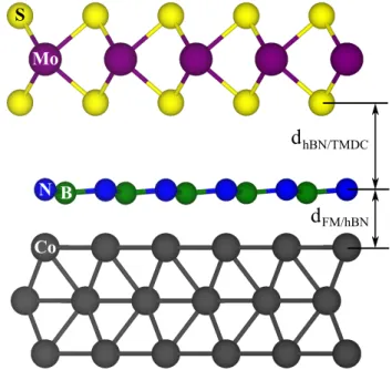
In Fig. 1 we show the geometry for MoS2/hBN/Co, as an exemplary structure. Initial atomic structures are set up with the atomic simulation environment (ASE)109, as follows. We choose a 4×4 supercell of the TMDC (MoS2,
Mo S
N B Co
dFM/hBN dhBN/TMDC
FIG. 1. (Color online) Side view of the TMDC/hBN/FM structure with labels for the atoms and distances. As an ex- ample, we show here MoS2/hBN/Co. The distances between the layersdFM/hBN anddhBN/TMDC are listed in Tab. II for all considered heterostructures.
WS2), a 5×5 cell of hBN, and a 5×5 cell of the FMs (Co, Ni). For the FM we take three monolayers of hcp Co or fcc(111) Ni. The hBN is placed above the FM, such that the nitrogen sits above the topmost Co/Ni atom, and the boron above the fcc-position above the FM slab, as found by previous studies19. The TMDC is placed such above the hBN/FM slab, that a transition metal atom (Mo, W) sits above a nitrogen atom. By choosing the heterostructure as explained, our unit cell contains 173 atoms, with a lattice constant ofa = 12.637 ˚A, for all of our considered hybrid geometries. For that we have to modify the lattice constants of the subsystem layers (TMDC, hBN, FM). In Tab. I we give an overview on the original experimental lattice constants, and the new modified lattice constants used for the heterostructures,
as well as the introduced strain. We can see that a max- imum strain of about 1.5% is present for Ni, being still acceptable for our purposes.
Co Ni hBN MoS2 WS2
a(exp.) [˚A] 2.507 2.492 2.504 3.150 3.153 a(het.) [˚A] 2.527 2.527 2.527 3.159 3.159
strain [%] 0.8 1.4 0.9 0.3 0.2
TABLE I. Overview of the lattice constants and strains for the subsystems used in the TMDC/hBN/FM heterostruc- tures. The experimental a (exp.) lattice constants (Refs.
110–114) of the bulk systems and lattice constants used for the heterostructuresa(het.) are given, along with the introduced strain for each subsystem, calculated as (ahet−aexp)/aexp. Note that for nickel, it is the lattice constant of a fcc(111) quasi-hexagonal surface.
To determine the interlayer distances, the atoms of the TMDC, hBN, and the top two Co/Ni layer atoms were allowed to relax only in their z positions (vertical to the layers). The average distances between the lay- ers dFM/hBN and dhBN/TMDC, as defined in Fig. 1, are listed in Tab. II for all considered geometries. The dis- tances are measured from the average position of the top Co/Ni (bottom S/Se) atoms, with respect to the average position of the N atoms of the hBN layer. The corru- gation of the hBN is on average 0.12 ˚A, independent of the heterostructure. The distancesdFM/hBNbetween the FMs and hBN are around 2.1 ˚A, indicating strong bond- ing. The distancesdhBN/TMDCbetween the hBN and the TMDCs are roughly 3.15 ˚A, being in the range of typical van der Waals distances. All these observations are in agreement with previous calculations of hBN on metal- lic substrates19,115,116, as well as TMDCs on hBN/metal interfaces64,65.
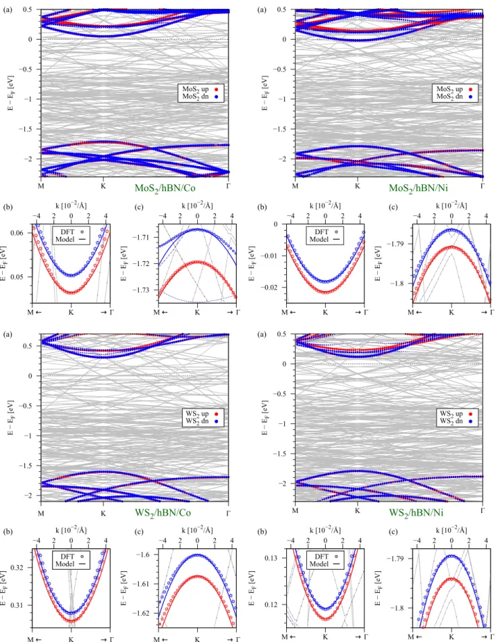
B. Band structure and fit results
In Fig. 2 we show the calculated band structures with- out SOC of all TMDC/hBN/FM heterostructures. Since a lot of bands are involved, originating from the hBN/FM substrate, we only show a projection of the bands origi- nating from the TMDC. In the following we analyze the case of MoS2/hBN/Co as a representative example. In Fig. 2(a) can see that the band structure closely resem- bles the bands of pristine MoS2. The Fermi level is lo- cated below the TMDC CB edge. Our calculated band structure is very different compared to other studies of proximity induced exchange55–57, where the TMDC ex- periences strong doping, probably due to the polar sur- faces of the substrates they consider. Note that a polar surface does not reflect a realistic situation, as surface re- constructions are present in real experiments. This can strongly modify the proximity exchange in experiments, as the hybridization with the substrate is the main ori-
gin of proximity exchange. Such effects are absent in a hBN/FM hybrid substrate, due to the hBN buffer layer.
Another advantage of our FM/hBN substrate is that the Curie temperature of the standard ferromagnets111 Co (TC= 1388 K) and Ni (TC= 627 K) is well above room temperature, allowing for experiments at ambient con- ditions. The ultimate goal is the spin injection into the TMDC via the hBN/FM tunnel junction. If we zoom to the fine structure around the K point, we find that the bands of the TMDC are spin split due to proximity exchange coupling, see Figs. 2(b,c). The splitting of the CB is smaller than that of the VB, both being in the few meV range.
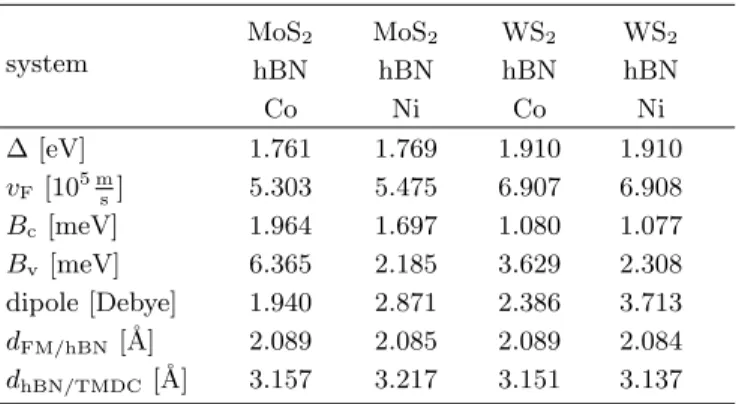
system
MoS2 MoS2 WS2 WS2
hBN hBN hBN hBN
Co Ni Co Ni
∆ [eV] 1.761 1.769 1.910 1.910
vF [105 ms] 5.303 5.475 6.907 6.908
Bc[meV] 1.964 1.697 1.080 1.077
Bv[meV] 6.365 2.185 3.629 2.308
dipole [Debye] 1.940 2.871 2.386 3.713 dFM/hBN[˚A] 2.089 2.085 2.089 2.084 dhBN/TMDC[˚A] 3.157 3.217 3.151 3.137
TABLE II. Summary of the fit parameters, calculated dipoles and distances for TMDC/hBN/FM systems without SOC.
The Hamiltonian used to fit these systems isH0+H∆+Hex, with ∆ as the orbital gap of the spectrum, the Fermi velocity vFandBcandBvare the proximity exchange parameters, re- spectively. The dipole of the structures is given in debye and dhBN/TMDCis the distance between hBN and the TMDC, and dFM/hBNis the distance between the FM and hBN, as defined in Fig. 1.
Since SOC effects are turned off, we can fit the band structure around the K point to our model Hamiltonian, neglecting for nowHsoc+HR. In Fig. 2(b,c), we can see that the bands are nicely reproduced by the model with the fit parameters given in Tab. II. However, we can see that there is a discrepancy between the model and the calculation, especially for the spin-down VB away from the K point. The case of MoS2/hBN/Co is the only one, where this happens. The origin of this is the hy- bridization of the VB spin-down state of MoS2 with Co d-states, as one can see in Fig. 2(a). In Tab. II we sum- marize our fit parameters for all considered heterostruc- tures. We notice, that especially the parameter Bv for the MoS2/hBN/Co case is very large, which is caused by the previously explained effect of hybridization. In a similar way, an earlier study has shown, that the hy- bridization with Cod-orbitals can strongly enhance the proximity exchange splitting in graphene on a hBN/Co substrate19. Note that also the value of the HubbardU, which shifts the Cod-levels in energy, affects the ’amount’
of hybridization and the spin splitting. Since we have consideredU = 1 eV only, we can only predict that such
−2
−1.5
−1
−0.5 0 0.5
M K MoS2/hBN/Ni Γ
(a)
(b) (c)
E − EF[eV] MoS2up
MoS2dn
−0.02
−0.01 0
M ← K →Γ
−4 2 0 2 4
E − EF[eV]
k [10−2/Å]
ModelDFT
−1.8
−1.79
M ← K →Γ
−4 2 0 2 4
E − EF[eV]
k [10−2/Å]
−2
−1.5
−1
−0.5 0 0.5
M K WS2/hBN/Co Γ
(a)
(b) (c)
E − EF[eV] WS2up
WS2dn
0.31 0.32
M← K →Γ
−4 2 0 2 4
E − EF[eV]
k [10−2/Å]
ModelDFT
−1.62
−1.61
−1.6
M← K →Γ
−4 2 0 2 4
E − EF[eV]
k [10−2/Å]
−2
−1.5
−1
−0.5 0 0.5
M K WS2/hBN/Ni Γ
(a)
(b) (c)
E − EF[eV] WS2up
WS2dn
0.12 0.13
M← K →Γ
−4 2 0 2 4
E − EF[eV]
k [10−2/Å]
ModelDFT
−1.8
−1.79
M← K →Γ
−4 2 0 2 4
E − EF[eV]
k [10−2/Å]
−2
−1.5
−1
−0.5 0 0.5
M K MoS2/hBN/Co Γ
(a)
(b) (c)
E − EF[eV] MoS2up
MoS2dn
0.05 0.06
M← K →Γ
−4 2 0 2 4
E − EF[eV]
k [10−2/Å]
ModelDFT
−1.73
−1.72
−1.71
M← K →Γ
−4 2 0 2 4
E − EF[eV]
k [10−2/Å]
FIG. 2. (Color online) Calculated band structures of TMDC/hBN/FM systems without SOC. (a) Band structure along high symmetry path M-K-Γ. The bands corresponding to the TMDC are highlighted in red (spin up) and blue (spin down). Bands originating from the hBN/FM substrate are plotted in grey. (b) Zoom to the CB edge originating from the TMDC around the K point. Symbols are DFT data and solid lines are the fit to the model Hamiltonian. (c) Same as (b), but for VB edge.
a hybridization is present in experiments, which leads to an enhanced spin splitting.
Unfortunately, we were not able to proper converge the calculations of the TMDC/hBN/FM heterostruc- tures including SOC effects. Therefore, we cannot be completely sure, whether the mentioned hybridization in the MoS2/hBN/Co structure will remain; the spin-orbit splitting in the TMDC VB is large38,117 and may shift the corresponding bands to much in energy to spoil the hybridization. However, a similar work of proximity ex- change in TMDC/CrI3heterostructures has shown, that inclusion of SOC barely affects the proximity exchange parameters61. Thus, we believe that proximity exchange on the order of 1–5 meV would still be present when in- cluding SOC for our TMDC/hBN/FM structures.
Similar to graphene/hBN/FM stacks19, we expect that the proximity exchange in the TMDCs also decreases with increasing number of hBN layers between the FM and the TMDC. Unfortunately, due to computational limitations (number of atoms in the supercell), we cannot study more than one hBN layer.
C. TMDC/hBN subsystems
Experimentally it is also interesting to consider the bare MoS2/hBN and WS2/hBN heterostructures, with- out any influence from the FM. For that, we take the TMDC/hBN/FM geometries, but remove the FM layers.
After subsequent relaxation, similar as described above,
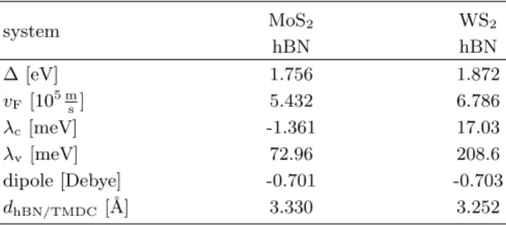
system MoS2 WS2
hBN hBN
∆ [eV] 1.756 1.872
vF[105 ms] 5.432 6.786
λc[meV] -1.361 17.03
λv[meV] 72.96 208.6
dipole [Debye] -0.701 -0.703
dhBN/TMDC[˚A] 3.330 3.252
TABLE III. Summary of the fit parameters, calculated dipoles and distances for TMDC/hBN systems with SOC. The Hamiltonian used to fit these systems isH0+H∆+Hsoc+HR, with ∆ as the orbital gap of the spectrum, the Fermi velocity vFandλcandλvare the SOC parameters. The distances are given as defined in Fig. 1.
we calculate the electronic band structures for thesubsys- tems, including SOC effects. The corrugation of the hBN reduces to about 20 pm on average, and the distances dhBN/TMDC between hBN and the TMDC are given in Tab. III for the TMDC/hBN stacks. The FM is respon- sible for the corrugation of the hBN layer, as already pointed out in earlier works19. Our model Hamiltonian is also suitable to describe this situation, when neglecting Hex.
−1
−0.5 0 0.5 1 1.5
M K Γ
(a)
(b) (c)
E − EF [eV] MoS2
hBN
1.28 1.29
M ← K → Γ
−4 2 0 2 4
E − EF [eV]
k [10−2/Å]
ModelDFT
−0.55
−0.5
−0.45
−0.4
M ← K → Γ
−4 2 0 2 4
E − EF [eV]
k [10−2/Å]
−0.5 0 0.5
< sz >
FIG. 3. (Color online) Calculated band structure of MoS2/hBN including SOC effects. (a) Band structure along high symmetry lines. The bands corresponding to MoS2
(hBN) are plotted in black (light-green). (b) Zoom to the CB edge. The color corresponds to thesz-expectation value.
Symbols are DFT data and solid lines are fits to the Model Hamiltonian. (c) Same as (b), but for VB edge.
The calculated band structure for MoS2/hBN is shown in Fig. 3. We find that we can perfectly reproduce the band structure around K and K’ valleys, with the fit pa- rameters given in Tab. III. The fit parameters for the TMDC/hBN heterostructures are nearly identical to the ones obtained for the bare TMDC monolayers38,117. We conclude that the hBN has effectively no impact on the TMDC dispersion and SOC.In principle, one would also expect Rashba SOC due to inversion symmetry break- ing, but from previous calculations of graphene/hBN/FM structures19, we conclude that the proximity induced SOC due to the hBN/FM substrate is negligible, com- pared to the proximity induced exchange and the giant intrinsic SOC of the bare TMDC38,117. Indeed, we find by fitting the model Hamiltonian to the band structure of the TMDC/hBN systems, thatHR can be neglected, as thesz spin expectation values of the bands near the K and K’ points almost do not differ from ±0.5, as we can see in Fig. 3.
In conclusion, the extracted proximity exchange (in- trinsic SOC) parameters from the calculations of the TMDC/hBN/FM (TMDC/hBN) systems, together with the Hamiltonian, can be used for further studies.
V. PROXIMITY EXCHANGE INDUCED VALLEY SPLITTING
The individually extracted parameters for proximity exchange and SOC, see Tabs. II and III, in combination with our model Hamiltonian can be used to calculate the low energy bands around K and K’ point with both effects present. We average the parameters forvF and ∆ from Tabs. II and III, for the MoS2and WS2based structures.
We take the SOC parameters for the two TMDCs from Tab. III, and the proximity exchange parameters from Tab. II. The full parameter sets are summarized in Tab.
IV, which we use for the following absorption spectra calculations.
system
MoS2 MoS2 WS2 WS2
hBN hBN hBN hBN
Co Ni Co Ni
∆ [eV] 1.759 1.763 1.891 1.891
vF[105 ms] 5.368 5.454 6.847 6.847 λc[meV] -1.361 -1.361 17.03 17.03
λv[meV] 72.96 72.96 208.6 208.6
Bc [meV] 1.964 1.697 1.080 1.077
Bv [meV] 6.365 2.185 3.629 2.308
s. part. [meV] 10.01 1.65 5.10 2.46
exciton [meV] 8.20 0.91 4.76 2.30
TABLE IV. Summary of the model Hamiltonian parameters, combined from Tabs. II and III. The orbital gap parameter ∆, the Fermi velocityvF,BcandBvare the proximity exchange parameters, and λc and λv are the SOC parameters. The valley splitting calculated from the single particle picture (s.
part.) and from the absorption spectra of the first exciton peak.
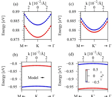
In this context, one can also generalize the exchange Hamiltonian55 to Hex = −mˆ ·s⊗(Bcσ+ +Bvσ−), with ˆm being a unit vector for the direction of the proximity exchange field and s is the vector contain- ing Pauli spin matrices. In Fig. 4 we show the calcu- lated model band structure employing the full Hamilto- nian with SOC and proximity exchange, setting ˆm= ˆmz, for the MoS2/hBN/Co heterostructure, using the param- eters from Tab. IV. Due to the combination of SOC and proximity exchange, time-reversal symmetry is bro- ken and the valley degeneracy is lifted, as can be seen when comparing the spin-split CB at K and K’, see Figs.
4(a,c). Remarkably, the order of the spin bands in the CB is the same for the two valleys. For bare TMDCs, the spin splitting in the CB is determined by the cor- responding SOC parameter λc. For the case of MoS2, we find that the SOC parameter is comparable in mag- nitude with the proximity exchange parameterλc≈Bc, due to the hBN/FM substrate. When the proximity ex- change is larger than the SOC, the band ordering of the spin-split CB is the same for both valleys, as can be seen
0.875 0.88 0.885 0.89
M ← K →Γ
2 0 2
Energy [eV]
k [10−2/Å]
−0.95
−0.9
−0.85
−0.8
M ← K →Γ
2 0 2
Energy [eV]
k [10−2/Å]
Model
0.875 0.88 0.885 0.89
M ← K’ →Γ
2 0 2
Energy [eV]
k [10−2/Å]
−0.95
−0.9
−0.85
−0.8
M ← K’ →Γ
2 0 2
Energy [eV]
k [10−2/Å]
−0.5 0 0.5
< sz>
(a) (c)
(b) (d)
FIG. 4. (Color online) Calculated model band structure em- ploying the full Hamiltonian, for MoS2/hBN/Co heterostruc- ture using parameters from IV. (a,b) Low energy CB and VB at K point. (c,d) Same as (a,b) but for K’ point.
in Figs. 4(a,c). In contrast, the VB SOC parameter is much larger than the corresponding proximity exchange parameterλv Bv, and the VB splitting is dominated by SOC.
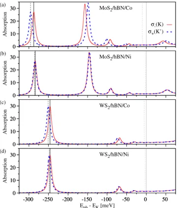
For a more realistic assessment of the proximity ex- change in the optical spectra, we investigate the valley splitting of the excitonic levels. Employing the parame- ters summarized in Table IV for the model Hamiltonian and the effective BSE, in Fig. 5 we show the calculated absorption spectra for the TMDC intralayer excitons.
For MoS2 systems, the B excitons are also visible (large peaks around -150 meV) and show a valley splitting with the same value as the A exciton but with opposite sign.
The extracted values for the valley splitting of the first exciton peak and within the single particle picture are summarized in Table. IV.
The optical excitation energy difference between K and K’ valley for MoS2/hBN/Co is giant, 8 meV, translating into about 50 T magnetic field for bare TMDCs, if as- suming 0.15 meV/T valley splitting49–52. A similar giant valley splitting of about 5 meV is achieved in the case of WS2/hBN/Co, translating to about 30 T magnetic field.
Remarkably, in the case of MoS2/hBN/Co, we have seen that proximity exchange together with band hybridiza- tion tod-orbitals causes a large VB splitting, leading to the giant valley splitting. In the case of WS2/hBN/Co, the valley splitting is also giant, but without any band hybridization effects. When Ni is considered as the FM, we find smaller valley splittings, 1 meV (7 T) for MoS2/hBN/Ni and 2.3 meV (15 T) for WS2/hBN/Ni, but still the corresponding magnetic fields are quite large, compared to the valley splittings achieved without prox- imity exchange.
0 10 20 (a) 30
MoS2/hBN/Co
Absorption
σ-(K) σ+(K’) 0
10 20 30
0 10 20 (b) 30
MoS2/hBN/Ni
Absorption
0 10 20 30
0 10 20 (c) 30
WS2/hBN/Co
Absorption
0 10 20 30
0 10 20 30
-300 -250 -200 -150 -100 -50 0 50
(d) WS2/hBN/Ni
Absorption
Eph - EK [meV]
0 10 20 30
-300 -250 -200 -150 -100 -50 0 50
FIG. 5. (Color online) Calculated absorption spectra for (a) MoS2/hBN/Co, (b) MoS2/hBN/Ni, (c) WS2/hBN/Co and (d) WS2/hBN/Ni. The vertical solid (dashed) lines indicate the energy contribution at K (K’) point. Vertical lines close to Eph−EK = 0 indicate the single-particle energies while the vertical lines at the first exciton peaks indicate the exci- tonic contribution. The energy difference betweenσ+andσ−
polarizations is the valley splitting, summarized in Table. IV.
VI. SUMMARY
We have calculated the band structures of TMDC/hBN/FM heterostructures and extracted valuable proximity exchange and SOC parameters, using a minimal low energy Hamiltonian. Due to the hBN buffer layer, the TMDC preserves a great degree of au- tonomy of its electronic structure. Proximity exchange is found to be on the order of 1–10 meV, depending on the specific FM. Especially in MoS2/hBN/Co, the spin splitting is giant, about 10 meV, due to proximity exchange and hybridization of Co d states with the spin-down VB of the TMDC. The excitonic absorption spectra, shows a giant splitting of the first exciton peak, translating into a valley polarization corresponding to tens of Tesla exchange field for bare TMDC monolayers.
The Ni-based heterostructures show less strong prox- imity exchange. We believe our calculations provide useful insight to interpret experimental properties of TMDC/hBN/(Co, Ni) devices, for instance related to spin injection, spin tunneling, and optics. Finally, our extracted parameters can be used as input for transport simulations and additional studies of excitonic effects.
ACKNOWLEDGMENTS
This work was supported by DFG SPP 1666, DFG SFB 1277 (project B05 and B07), the European Unions Hori- zon 2020 research and innovation program under Grant No. 785219, the Alexander von Humboldt Foundation and Capes (grant No. 99999.000420/2016-06).
∗ klaus.zollner@physik.uni-regensburg.de
1 I. ˇZuti´c, J. Fabian, and S. Das Sarma, Rev. Mod. Phys.
76, 323 (2004).
2 W. Han, R. K. Kawakami, M. Gmitra, and J. Fabian, Nat. Nano.9, 794 (2014).
3 J. Fabian, A. Matos-Abiague, C. Ertler, P. Stano, and I. ˇZuti´c, Acta Phys. Slov.57, 342 (2007).
4 W. Liu, P. K. J. Wong, and Y. Xu, Prog. Mater. Sci.99, 27 (2019).
5 N. Briggs, S. Subramanian, Z. Lin, X. Li, X. Zhang, K. Zhang, K. Xiao, D. Geohegan, R. Wallace, L.-Q. Chen, M. Terrones, A. Ebrahimi, S. Das, J. Redwing, C. Hinkle, K. Momeni, A. van Duin, V. Crespi, S. Kar, and J. A.
Robinson, 2D Mater.6, 022001 (2019).
6 J. H. Zhiquan Yuan and K. Liu, Crystals7, 265 (2017).
7 Z. Hu, Z. Wu, C. Han, J. He, Z. Ni, and W. Chen, Chem.
Soc. Rev.47, 3100 (2018).
8 M. V. Kamalakar, A. Dankert, J. Bergsten, T. Ive, and S. P. Dash, Sci. Rep.4, 6146 (2014).
9 W. Fu, P. Makk, R. Maurand, M. Br¨auninger, and C. Sch¨onenberger, J. Appl. Phys.116, 074306 (2014).
10 M. Dr¨ogeler, C. Franzen, F. Volmer, T. Pohlmann, L. Banszerus, M. Wolter, K. Watanabe, T. Taniguchi,
C. Stampfer, and B. Beschoten, Nano Letters16, 3533 (2016).
11 M. Dr¨ogeler, F. Volmer, M. Wolter, B. Terr´es, K. Watan- abe, T. Taniguchi, G. G¨untherodt, C. Stampfer, and B. Beschoten, Nano Lett.14, 6050 (2014).
12 M. V. Kamalakar, A. Dankert, P. J. Kelly, and S. P.
Dash, Sci. Rep.6, 21168 (2016).
13 M. V. Kamalakar, C. Groenveld, A. Dankert, and S. P.
Dash, Nat. Commun.6, 6766 (2015).
14 M. Gurram, S. Omar, and B. J. van Wees, 2D Materials 5, 032004 (2018).
15 M. Gurram, S. Omar, and B. J. van Wees, Nat. Commun.
8, 248 (2017).
16 L. Banszerus, M. Schmitz, S. Engels, J. Dauber, M. Oellers, F. Haupt, K. Watanabe, T. Taniguchi, B. Beschoten, and C. Stampfer, Sci. Adv.1, 1 (2015).
17 N. Petrone, C. R. Dean, I. Meric, A. M. Van Der Zande, P. Y. Huang, L. Wang, D. Muller, K. L. Shepard, and J. Hone, Nano Lett.12, 2751 (2012).
18 V. E. Calado, S. E. Zhu, S. Goswami, Q. Xu, K. Watan- abe, T. Taniguchi, G. C. Janssen, and L. M. Vander- sypen, Appl. Phys. Lett.104(2014), 10.1063/1.4861627.