Theory of proximity-induced exchange coupling in graphene on hBN/(Co, Ni)
Klaus Zollner, Martin Gmitra, Tobias Frank, and Jaroslav Fabian Institute for Theoretical Physics, University of Regensburg, 93040 Regensburg, Germany
(Received 27 July 2016; published 24 October 2016)
Graphene, being essentially a surface, can borrow some properties of an insulating substrate (such as exchange or spin-orbit couplings) while still preserving a great degree of autonomy of its electronic structure. Such derived properties are commonly labeled as proximity. Here we perform systematic first-principles calculations of the proximity exchange coupling, induced by cobalt (Co) and nickel (Ni) in graphene, via a few (up to three) layers of hexagonal boron nitride (hBN). We find that the induced spin splitting of the graphene bands is of the order of 10 meV for a monolayer of hBN, decreasing in magnitude but alternating in sign by adding each new insulating layer. We find that the proximity exchange can be giant if there is a resonantdlevel of the transition metal close to the Dirac point. Our calculations suggest that this effect could be present in Co heterostructures, in which adlevel strongly hybridizes with the valence-band orbitals of graphene. Since this hybridization is spin dependent, the proximity spin splitting is unusually large, about 10 meV even for two layers of hBN.
An external electric field can change the offset of the graphene and transition-metal orbitals and can lead to a reversal of the sign of the exchange parameter. This we predict to happen for the case of two monolayers of hBN, enabling electrical control of proximity spin polarization (but also spin injection) in graphene/hBN/Co structures.
Nickel-based heterostructures show weaker proximity effects than cobalt heterostructures. We introduce two phenomenological models to describe the first-principles data. The minimal model comprises the graphene (effective)pzorbitals and can be used to study transport in graphene with proximity exchange, while thepz-d model also includes hybridization withdorbitals, which is important to capture the giant proximity exchange.
Crucial to both models is the pseudospin-dependent exchange coupling, needed to describe the different spin splittings of the valence and conduction bands.
DOI:10.1103/PhysRevB.94.155441 I. INTRODUCTION
Graphene is a diamagnet with a weak spin-orbit coupling, so spin interactions in devices containing clean graphene are rather weak [1]. One way to enhance these interactions is by functionalizing graphene with adatoms and admolecules, which works well for both exchange [2–7] and spin-orbit [7–16] couplings. Functionalized graphene has local “hot spots” of giant exchange and spin-orbit fields, which can be used to investigate spin transport [17–22].
A promising way to induce exchange coupling in graphene is placing it on a ferromagnetic substrate. In order to preserve the Dirac band structure, the substrate should be a ferromag- netic insulator, as in the density functional theory (DFT) study of graphene on EuO [23], predicting 20% spin polarization of graphene bands, an antiferromagnetic insulator [24], or a ferromagnetic metal separated from graphene by an insulating barrier. The advantage of this approach over functionalizing graphene with adatoms is that the induced band structure effects are uniform; one can speak of a proximity electronic band structure with the hope of further electrical control.
In fact, heterostructures of graphene with ferromagnets are essential for introducing spintronic phenomena [25,26] in graphene. Proximity exchange in graphene on a ferromagnetic insulator has recently been experimentally investigated for spin transport [27–29], while tunnel junctions of graphene with ferromagnetic metals have been widely used in experimental demonstrations of electrical spin injection into graphene [30–
40]. The benefits turn out to be mutual: graphene can protect ferromagnets from oxidation and yield large spin tunneling sig- nals in ferromagnet/graphene interfaces [41,42], in agreement with theory [43,44]. It is also predicted that graphene on Co can strongly enhance the perpendicular magnetic anisotropy [45].
In this paper we present systematic first-principles investi- gations of the proximity exchange in graphene on a substrate comprising either Co or Ni and an hBN tunnel barrier. The barrier shields the Dirac bands from strong hybridization with the metallic orbitals, but it also induces an orbital gap due to the sublattice symmetry breaking [46]. The predicted band gap of a graphene/hBN structure is of the order of 50 meV and may be essential for building graphene-based field-effect transistor devices [47]. The proximity of graphene and metals can lead to doping due to the different work functions and resulting charge transfer, as studied from first principles in Refs. [48,49].
A recent study has predicted that graphene on (hBN)/Co can be effectively gated, and the induced spin polarization can be tuned by a transverse electric field [50].
We have studied tunnel structures of graphene and (Co, Ni) with up to three layers of hBN. For a single tunneling layer, the proximity-induced exchange in the Dirac bands is about 10 meV. The resulting spin splitting depends on the band (valence and conduction), which has motivated us to introduce a pseudospin-dependent exchange-coupling model of graphene’spzorbitals. This minimal model nicely explains the DFT data. As we increase the number of hBN layers, the proximity exchange is expected to decrease exponentially.
However, we observe that in the case of two hBN layers on Co, the valence band of graphene remains spin split by about 10 meV. This giant splitting is due to a Cod orbital of energy close to the Dirac point that strongly couples to thepz graphene orbitals. As thisd orbital is spin polarized, the resulting anticrossing of the corresponding bands is seen as a giant spin splitting ofpz orbitals. We then propose an extended effective model based onpzanddorbitals to explain the hybridization-induced spin splitting. Certainly, this effect
can be, to a certain degree, an artifact of DFT, as thedlevels need not be well described, so in the discussion we also look at the HubbardUeffects on the proximity structure. We indeed find that the strong hybridization is reduced. ForU=1 the valence-band splitting reduces to about 5 meV, which is still giant when compared with the spin splitting of 0.2 meV of the conduction band. We therefore believe that this giant enhancement of proximity exchange in Co-based devices with two hBN layers could be observed. In the Ni-based structures that we studied, this effect is absent.
As the number of hBN layers increases one by one, the proximity exchange changes sign. This is reminiscent of the interlayer coupling in ferromagnet/metal/ferromagnet structures, in which the coupling strength between the two ferromagnets is an oscillating function of the spacer thick- ness [51]. Another means to change the proximity exchange is to apply a transverse electric field. However, we find that in most (of our investigated) cases mainly the orbital parameters (staggered potential and Dirac point offset from the Fermi level) are affected. The exchange parameters change much less. The notable exception is the aforementioned slab of graphene and Co, with two hBN layers. Here the proximity exchange is strongly affected by the position of thed orbitals of Co, so the electric field leads to a strong modification of the induced spin polarization in graphene. We even observe a crossover at electric fields close to 2 V/nm, where the sign of the exchange changes, making electrical control of the orientation of the (equilibrium) proximity spin polarization in graphene possible. Finally, we investigate the proximity effects with respect to the number of ferromagnetic layers, finding that three layers are already representative of the bulk.
We also give magnitudes of the induced spin splitting of the hBN valence and conduction bands, which are active in spin-dependent tunneling.
Our investigations should be useful for interpreting spin injection and spin tunneling data in graphene/hBN/(Co, Ni) devices. Especially in cases of thin tunnel barriers (one or two monolayers of hBN), there could be a sizable equilibrium spin polarization in graphene underneath the ferromagnetic electrodes. The proposed models could be used for simulations of spin transport in graphene with proximity exchange.
Overall, we find that Co is more interesting than Ni, as far as the proximity effects go, with Ni showing weaker proximity exchange effects and no signatures of giant spin-dependent hybridization between Nidorbitals and graphenepzones.
This paper is organized as follows. In Sec.IIwe describe the computational methods and the investigated graphene/hBN/Co structures in detail. In Sec. III we introduce two model Hamiltonians describing the proximity Dirac bands. In Sec.IV we present the DFT results for graphene/hBN/(Co, Ni) slabs.
There we also discuss the behavior of the proximity band structure in the presence of more hBN layers and in the presence of a transverse electric field, as well as effects of the HubbardUand the thickness of the ferromagnetic layer.
II. COMPUTATIONAL METHODS AND SYSTEM DEFINITION
To study proximity-induced exchange interaction in graphene we consider a graphene/insulator/ferromagnet het-
erostructure in a slab geometry. Electronic states were calcu- lated using DFT [52] within theQUANTUM ESPRESSOsuite [53].
Self-consistent calculations were performed with a k-point sampling of 120×120×1, if not indicated otherwise, in order to get the correct Fermi energy of the metal and to obtain an accurate description of bands in an energy window of±1 eV around the Fermi level [54]. Open-shell calculations provide the spin-polarized ground state. We used an energy cutoff for charge density of 450 Ry, and the kinetic-energy cutoff for wave functions was 100 Ry for the scalar relativistic pseu- dopotential with the projector augmented-wave method [55]
with the Perdew-Burke-Ernzerhof exchange-correlation func- tional [56]. For the relaxation of the heterostructures, we added van der Waals corrections [57] and used the Broyden-Fletcher- Goldfarb-Shanno quasi-Newton algorithm [58]. In order to simulate quasi-two-dimensional systems a vacuum of 15 ˚A was used together with dipole corrections [59] to avoid interactions between periodic images in our slab geometry. To determine the interlayer distances, the atoms were allowed to relax in theirzpositions (transverse to the layers) until all components of all forces were reduced below 10−4(Ry/a0), wherea0is the Bohr radius.
Initial atomic structures were set up with the atomic simulation environment (ASE) [60], as follows. The lattice constant of graphene isa=2.46 ˚A [61], the one for hBN isa = 2.504 ˚A [62], and the one for hcp cobalt isa=2.507 ˚A [63].
We fix an effective average lattice constant ofa=2.489 ˚A for this well-lattice-matched system, as a compromise to make the lattices commensurable and to keep the unit cell as small as possible. The lattice of graphene is strained by only 1%.
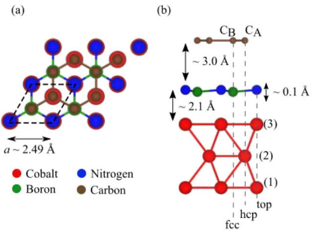
We tested different stacking possibilities and found the energetically preferential structure. In Fig. 1, we show our definition of the unit cell of the graphene/hBN/Co structure.
A computational unit cell contains two carbon atoms, CAand CB, forming graphene; one boron atom and one nitrogen atom
Cobalt Nitrogen
Boron Carbon (1)
(2) (3) CB CA
~ 2.1 Å
~ 3.0 Å
~ 0.1 Å
(a) (b)
top fcchcp a ~ 2.49 Å
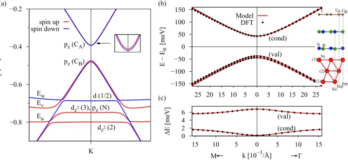
FIG. 1. Structure of the graphene/hBN/Co system, with labels for the different atoms. (a) Top view of the structure, with one unit cell emphasized by the dashed line. (b) Side view with stacking configuration: CB is over boron, and CA is over hBN hexagon.
Nitrogen is at the top site above Co, and boron is above the fcc site of Co. The distances indicated are measured between graphene/Co and the nitrogen atom of hBN since the hBN layer is slightly corrugated by z=0.113 ˚A. The boron atom is closer to the Co surface. Numbers in parentheses indicate the Co layer.
per hBN layer; and three cobalt atoms, one per atomic layer. In general, three positions (top, hcp, and fcc) can be distinguished within a hexagonal unit cell. The different positioning possibil- ities of the carbon atoms above the substrate will influence the strength of the proximity magnetism. We get the lowest-energy configuration when nitrogen atoms are at the top sites and boron atoms are at the fcc sites above Co. Carbon atoms sit on top of boron atoms and at the hollow position above hBN (see Fig.1).
These findings are in agreement with previous DFT studies [46,64,65]. After relaxation of atomic positions we obtained layer distances of dCo/hBN=2.099 ˚A between the cobalt and hBN and dhBN/Gr=3.010 ˚A between hBN and graphene (measured between C/Co and N atoms, respectively, since the hBN layer is corrugated). The layer distances of this minimum energy configuration are roughly in agreement with those in Refs. [46,65,66], which reportdhBN/Gr=3.22–3.40 ˚A anddCo/hBN=1.92–2.02 ˚A. We also find that the hBN layer is not flat anymore but slightly buckled since the boron atom is closer to the Co surface by 0.113 ˚A compared to the nitrogen atom, in agreement with Refs. [65,67].
For the stacking of hBN itself, when we use more than one monolayer of hBN, we use an AA stacking (B over N, N over B), which is the energetically favorable one, as shown in Ref. [68], with distances between the layers in the range ofdhBN/hBN=2.98–3.09 ˚A (details are given in Secs.IV A 2 andIV A 3).
III. EFFECTIVE HAMILTONIAN
Our main goal is to answer the question, how do hBN and the ferromagnetic substrate affect the graphene Dirac cone at K?
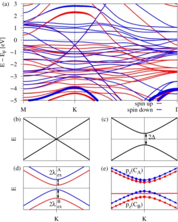
In Fig. 2(a) we show the calculated spin-resolved band structure of the graphene/hBN/Co system (see Fig.1), along the high-symmetry path M-K-in the energy window from
−5 to 3 eV. We can see that the linear dispersion of graphene around the K point is preserved and that the Dirac point is roughly−0.5 eV below the system Fermi level. Other bands, especially those in the vicinity of the Dirac point energyED, originate mainly from thed states of the ferromagnet which are located around the Fermi energy. The bands at the K point originating from hBN are far away from the Dirac point, with the highest- (lowest-) lying valence (conduction) band located at−4 eV (2 eV) away from the system Fermi level, emphasized by thicker lines in Fig. 2(a). Moreover, hBN becomes spin polarized: its bands spin split by about 0.5 eV.
A. Minimalpzmodel
We introduce a minimal Hamiltonian to describe the proximity-induced exchange spin splitting in graphene, sim- ilar to earlier derivations of effective Hamiltonians for the proximity spin-orbit coupling in graphene on transition-metal dichalcogenides [69,70] and on the Cu(111) substrate [49].
Pristine graphene is described by the massless Dirac HamiltonianH0in the vicinity of K (K):
H0 =vF(τ σxkx+σyky), (1)
FIG. 2. Band structure of the graphene/hBN/Co system. (a) Calculated spin-resolved band structure along the high-symmetry path M-K-using DFT. Spin-up (-down) states are shown in solid red (blue). Thicker bands at energies smaller (larger) than−4 eV (2 eV) correspond to the highest- (lowest-) lying valence (conduction) band of hBN which is spin split. (b) Hamiltonian H0 gives the linear dispersion of graphene with vF defining the slope. (c) H0+H
describes gapped graphene with a gap of 2. (d)H0+H+Hex
describes gapped graphene in which the spin degeneracy of the conduction (valence) band gets lifted with a splitting of 2λAex(2λBex). (e) Close-up of the band structure from (a) around the K point with labels for the different orbital and sublattice contributions of graphene; that is, the upper (lower) two bands are formed bypzorbitals of sublattice A (B).
wherevFdenotes the Fermi velocity,kxandkyare the Cartesian components of the electron wave vector measured from K (K), andσxandσy are the pseudospin Pauli matrices acting on the A and B sublattice orbitals. HamiltonianH0describes gapless Dirac states with conical dispersion near Dirac points, with τ = ±1 for the K (K) point, shown in Fig.2(b).
Since graphene is on a hBN/Co substrate, the carbon atoms from different sublattices feel different potentials, leading to the Hamiltonian
H=σzs0, (2) withσzbeing the pseudospin Pauli matrix,s0 being the unit spin matrix, andbeing the proximity-induced orbital gap of the spectrum. The HamiltonianHdescribes a mass term, which breaks the pseudospin symmetry, and thus H0+H
describes a gapped graphene dispersion, shown in Fig.2(c).
To study the proximity exchange, we introduce the Hamil- tonian
Hex=λAex[(σz+σ0)/2]sz
+λBex[(σz−σ0)/2]sz, (3) withλAexandλBexbeing the exchange parameters for sublattices A and B, respectively. The dispersion of the HamiltonianH0+ H+Hexis shown in Fig.2(d), along with the spin character.
This term is similar to a sublattice-resolved intrinsic spin-orbit coupling Hamiltonian [9,11,16,49,69,70]. The only difference is that it breaks time-reversal symmetry, associated with the magnetization. A close-up in the vicinity of the K point of the DFT band structure is shown in Fig2(e), supporting the need for a sublattice-resolved exchange Hamiltonian.
The proximity exchange (pex) Hamiltonian,
Hpex=H0+H+Hex, (4) is a minimal model using only effective carbon pz orbitals, which can be used to fit the DFT data directly at the K point and extract the pure band splittings. This Hamiltonian can be used for model charge and spin transport calculations. The parameters,λAex, andλBexare related to the band splittings at the K point: splitting of the conduction bandsEcond= |2λAex|,
splitting of the valence bandsEval= |2λBex|, and orbital gap Econd−val= |2|, as shown in Figs.2(c)and2(d).
The Dirac point is shifted in energy with respect to the system Fermi level by an energyED, as can be seen in Fig.2(a).
We call the energyEDthe Dirac point energy, and it will be our measure for the doping level. The Dirac point energyEDfor this model is calculated by averaging the four DFT energies of the graphene Dirac bands at the K point.
B. Extendedpz-dHamiltonian
The DFT results in Fig.2(a)show that in the interesting range of energies of the graphene Dirac bands, there can also lie flat d orbitals from Co. When these orbitals hybridize withpz carbon orbitals in graphene, the effective exchange coupling gets strongly modified. In order to capture this effect quantitatively, we extend our minimal model by a set of d orbitals that appear close to the Dirac point. Similar effects occur in graphene on the Cu(111) substrate [49], for example.
Figure2(a)shows that in the energy window of±400 meV from the Dirac point, three d bands interact with the Dirac states. We then extend our model by adding an effective ferromagnet HamiltonianHFM, consisting of threed bands, which describes the hybridization of the ferromagnetdbands with the graphene states. The full effective Hamiltonian in the basis|A↑,|A↓,|B↑,|B↓,u,v,w, where u, v, and w label the threed orbitals (of the spin specified by the DFT), reads
Hpz-d =H0+H+Hex+HFM=
⎛
⎜⎜
⎜⎜
⎜⎜
⎜⎜
⎜⎜
⎜⎜
⎜⎝
˜ +λ˜Aex 0 vF(kx−iky) 0 uA↑ vA↑ wA↑ 0 ˜ −λ˜Aex 0 vF(kx−iky) uA↓ vA↓ wA↓
vF(kx+iky) 0 −˜ −λ˜Bex 0 uB↑ vB↑ wB↑
0 vF(kx+iky) 0 −˜ +λ˜Bex uB↓ vB↓ wB↓
uA↑ uA↓ uB↑ uB↓ Eu 0 0
vA↑ vA↓ vB↑ vB↓ 0 Ev 0
wA↑ wA↓ wB↑ wB↓ 0 0 Ew
⎞
⎟⎟
⎟⎟
⎟⎟
⎟⎟
⎟⎟
⎟⎟
⎟⎠ .
(5)
HereEj,j =u, v, w, are the energies that correspond to the d states, andj↑A,B,↓ are the effective hybridization parameters with the corresponding Dirac state, where the subscript (su- perscript) indicates the spin (pseudospin) state. The proximity exchange (˜λex) and orbital gap ( ˜) parameters are, in principle, different from those of the minimal HamiltonianHpex, as they are renormalized due to the hybridization. The hybridization parameters vanish if the Dirac states directly at K are relatively far from the d bands. As soon as the Dirac states at K are close to a d band or the hybridization is so large that it affects the Dirac states, we can describe the hybridization with the corresponding interaction parameter. We call the Hamiltonian Hpz-d the pz-d model. The energy window of roughly ±150 meV from the Dirac point energy can be described by this model rather well (see Figs.3and4).
The pz-d model describes the hybridization between the surface d bands of Co with the graphene Dirac states. As we will discuss, this hybridization significantly enhances the
effective proximity exchange splitting. Like the minimal model Hpex, thepz-d model has to be shifted in energy to match the DFT data. We call this energyE0, and it is an analog ofED.
IV. PROXIMITY EXCHANGE INTERACTION We present our DFT calculations of the proximity exchange in graphene/hBN/Co and graphene/hBN/Ni for one, two, and three layers of hBN, as well as fits to the effective Hamilto- nians. The proximity exchange decreases in magnitude but oscillates as the number of layers changes by one. This oscillating behavior is reminiscent of the oscillatory magnetic interlayer coupling [51,71].
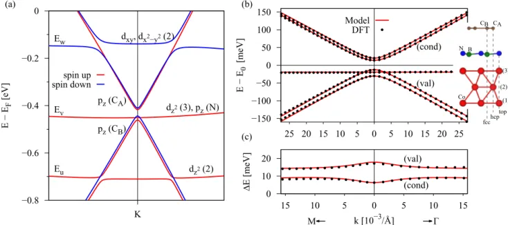
A. Graphene/hBN/cobalt 1. One hBN layer
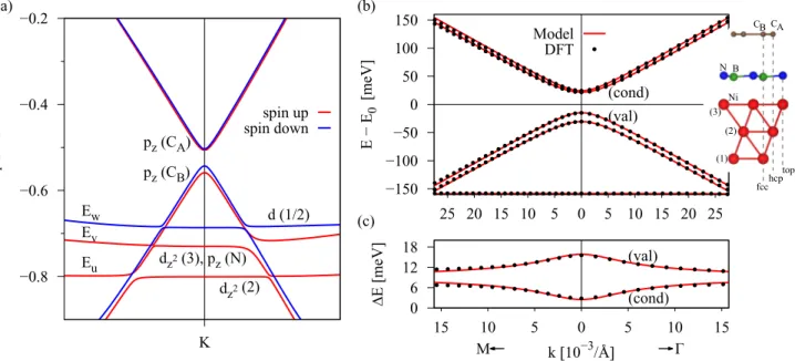
Figure3(a)shows the spin-polarized band structure of the graphene/hBN/Co heterostructure for one layer of hBN. The
−0.8
−0.6
−0.4
−0.2 0
K
E − EF[eV] pz(CA)
pz(CB)
dz2(3), pz(N)
dz2(2) dxy, dx2−y2(2)
(a) (b)
(c)
Eu Ev Ew
spin up spin down
−150
−100
−50 0 50 100 150
25 20 15 10 5 0 5 10 15 20 25 E − E0[meV]
(cond)
(val) Model
DFT
0 10 20
15 10 5 0 5 10 15
E [meV]
k [10−3/Å]
(val)
(cond)
M
(1) (2)
(3) CB CA
top fcchcp N B
Co
FIG. 3. Calculated spin-polarized band structure of the graphene/hBN/Co heterostructure for one layer of hBN. (a) Band structure in the vicinity of the Dirac point with labels for the main orbital contributions from which the individual bands are formed; for example,dz2(3) corresponds to thedz2orbital of Co atom (3) from Fig.1. LabelsEj,j=u, v, w, are the energy bands, which correspond to the Codstates used to fit thepz-dmodel Hamiltonian in Eq. (5). The energiesEj, in Eq. (5), are measured with respect to the energyE0. (b) The fit to the pz-dmodel with a side view of the structure. First-principles data (dotted lines) are well reproduced by thepz-dmodel (solid lines). (c) The corresponding splittings of the valence (val) and conduction (cond) Dirac states of graphene. The main fit parameters areE0= −430.89 meV, ˜ =21.45 meV, ˜λAex= −7.63 meV, ˜λBex=8.95 meV,Eu= −279.41 meV,Ev= −19.37 meV,Ew=282.31 meV, wA↓=48.44 meV. The most relevant parameters are obtained by a least-squares fit, minimizing the difference between the model and the DFT data for a fitting range from K towards thepoint forkpoints up to 20×10−3/A. By performing the fit towards the M point, one would obtain slightly different (by at most˚ 5%) parameters. From the band structure and from the fact that we limit our fitting range, we find that no additional hybridization parameters j↑A,B,↓ are necessary to fit our band structure, except for the mentioned ones. The Fermi velocity to match the slope away from the K point is vF=0.812×10⁶m/s, which corresponds to a nearest-neighbor hopping parameter oft=2.48 eV, slightly smaller than the commonly used value of 2.6 eV [9,11,16] due to the larger lattice constant used here.
−0.8
−0.6
−0.4
−0.2 0
K E − EF[eV]
pz(CA) pz(CB)
dz2(3), pz(N)
dz2(2) dxy, dx2−y2(2)
(a) (b)
(c)
Eu Ev Ew
spin up spin down
−150
−100
−50 0 50 100 150
25 20 15 10 5 0 5 10 15 20 25 E − E0[meV]
(cond)
(val) Model
DFT
0 10 20
15 10 5 0 5 10 15
E [meV]
k [10−3/Å]
(val) (cond)
M
N B
Co (1)
(2) (3) CA CB
top fcchcp
FIG. 4. Spin-polarized band structure of the graphene/hBN/Co heterostructure for two layers of hBN (AAstacking). (a) Band structure in the vicinity of the Dirac point with labels for the main orbital contributions. The inset shows a close-up of the conduction Dirac states to visualize the reversal of the spin states. (b) The fit to thepz-dmodel with a side view of the structure for two layers of hBN. DFT data (dotted lines) are well reproduced by thepz-dmodel (solid lines). (c) The corresponding splittings of the valence and conduction Dirac states. The fit parameters areE0= −352.65 meV, ˜=41.02 meV, ˜λAex=0.096 meV, ˜λBex= −0.512 meV,Eu= −357.12 meV,Ev= −114.75 meV,Ew=207.34 meV, vB↑=41.67 meV. The Fermi velocity to match the slope away from the K point isvF=0.820×10⁶m/s. All other parameters are zero for the same fitting range as for the one-layer case.
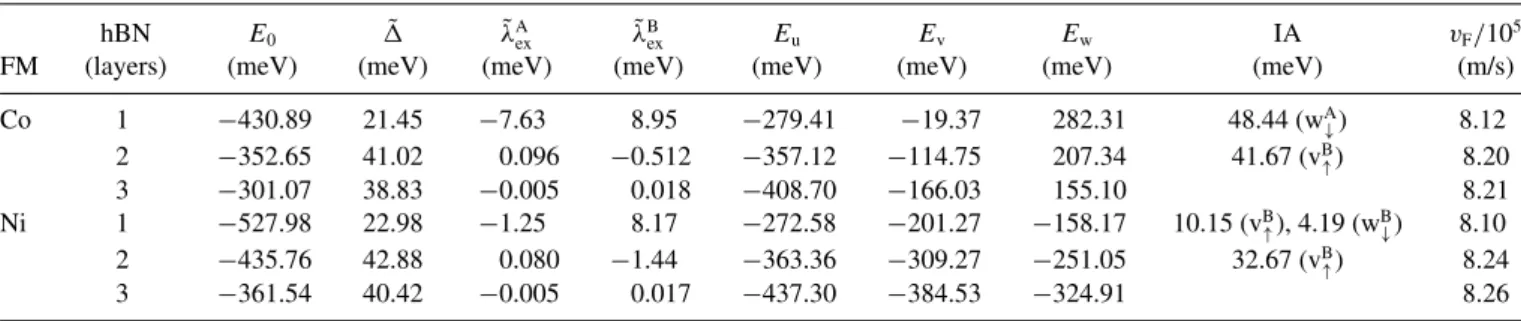
TABLE I. Summary of the most relevant parameters for all relevant structures (a=2.489 ˚A andU=0 eV) for the different ferromagnets (FM) Co and Ni for one to three layers of hBN: proximity gap ˜; energy shiftE0; exchange parameters ˜λAexand ˜λBex; energiesEu,Ev, andEw
of the interacting ferromagnet bands; and the interaction parameters (IA) necessary to fit the DFT data of the corresponding structure with the pz-dmodel HamiltonianH, Eq. (5).
hBN E0 ˜ λ˜Aex λ˜Bex Eu Ev Ew IA vF/105
FM (layers) (meV) (meV) (meV) (meV) (meV) (meV) (meV) (meV) (m/s)
Co 1 −430.89 21.45 −7.63 8.95 −279.41 −19.37 282.31 48.44 (wA↓) 8.12
2 −352.65 41.02 0.096 −0.512 −357.12 −114.75 207.34 41.67 (vB↑) 8.20
3 −301.07 38.83 −0.005 0.018 −408.70 −166.03 155.10 8.21 Ni 1 −527.98 22.98 −1.25 8.17 −272.58 −201.27 −158.17 10.15 (vB↑), 4.19 (wB↓) 8.10 2 −435.76 42.88 0.080 −1.44 −363.36 −309.27 −251.05 32.67 (vB↑) 8.24
3 −361.54 40.42 −0.005 0.017 −437.30 −384.53 −324.91 8.26
graphene Dirac states forspin up are lying lower in energy than the spin-down ones. The Dirac point energy is below the system Fermi level, corresponding to electron doping of graphene, since the Fermi level now crosses the conduction band of graphene. This shift is induced by the metal, as already suggested in Ref. [48]. The Co bands hybridize with the graphene states in the vicinity of the K point and introduce exchange splitting.
From the band structure in Fig. 3 we see that the linear dispersion of graphene is preserved. In addition, a gap forms, and the spin degeneracy of the Dirac states gets lifted, allowing for semiconducting properties along with the usage of different spin channels by appropriate experimental setups.
By comparing our DFT results to thepz-dmodel Hamiltonian Hpz-d, Eq. (5), we obtain the parameters given in TableIfor Co as the ferromagnet and one layer of hBN. The fit of the pz-d model is shown in Fig.3(b)and agrees very well with the DFT data. The gap in the dispersion is found to be roughly 40 meV, while the band splittings are of the order of 10 meV for one layer of hBN.
We additionally employ the minimalHpexmodel, Eq. (4), valid directly at the K point. The parameters for the minimal pz model are given in Table II. The two models yield quantitatively very similar exchange parameters due to the rather weak hybridization of thedorbitals with graphene ones.
2. Two hBN layers
Figure 4 shows the calculated band structure and the fit to thepz-d model in the case of two layers of hBN and three layers of Co. The inset in Fig.4(b)shows the geometry for two TABLE II. Summary of the most relevant parameters for all relevant structures (a=2.489 ˚A andU=0 eV) for the different ferromagnets (FM) Co and Ni for one to three layers of hBN:
proximity gap, Dirac point energyED, and the exchange parameters λAexandλBexnecessary to fit the DFT data of the corresponding structure with the minimalpzmodel Hamiltonian, Eq. (4).
FM hBN (layers) ED(meV) (meV) λAex(meV) λBex(meV)
Co 1 −433.10 19.25 −3.14 8.59
2 −348.03 36.44 0.097 −9.81
3 −301.10 38.96 −0.005 0.018
Ni 1 −527.89 22.86 −1.40 7.78
2 −434.82 42.04 0.068 −3.38
3 −361.57 40.57 −0.005 0.017
layers of hBN. The relative position of carbon atom CAto hBN is not changed, while the position of atom CBis changed, such that it is again on top of the uppermost boron atom, which is the energetically favorable situation for graphene on hBN. The conduction (valence) Dirac states are still formed by sublattice A (B), even though CB has changed its position within the unit cell. The layer distance between the two hBN layers was relaxed todhBN/hBN =2.977 ˚A, and the distance between the uppermost hBN layer and graphene isdhBN/Gr=3.114 ˚A in the two-hBN-layer case. The corrugation of the lower hBN and the distance between hBN and Co did not change.
Figure 4(a) shows the spin-polarized band structure of graphene/hBN/Co for two layers of hBN. In the band structure, now, the spin-up graphene Dirac states are no longer lying lower in energy than the spin-down ones, leading to a reversal of the sign of the exchange parametersλAexandλBex. The band structure shows that the doping level decreases by roughly 80 meV, and the hybridization with thed band with energy Ev, coming from the top Co layer, is strongly enhanced, in contrast to the one-hBN-layer case. The perfect fit to thepz-d model is also seen in Fig.4(b); the obtained parameters are given in TableIfor Co as the ferromagnet and two layers of hBN. In Fig.4(c)we can see that the band splitting at the K point of the conduction (valence) bands is smaller (larger) than in the one-hBN-layer case. In addition, the proximity-induced gap nearly doubles, and the hybridization to the Codz2(3) state is much stronger.
The inset in Fig.4(b)shows that for the case of two hBN layers, carbon atom CB (now at the top site above Co) has a direct connection to the Co atom in the top position via a nitrogen atom and a boron atom of the two individual hBN layers. Localized at this Co atom in the top position, there is some density withdz2 character (resulting in the band with energyEv) which can propagate through this direct path and polarize carbon atom CB. This hybridization is described by the parameter vB↑, shifting the corresponding bands in energy and leading to the opening of a hybridization gap in the band structure. The vertical stacking of the atoms facilitates the hybridization of the carbonpz states with Cod states. For the case of one hBN layer there is no direct path connecting Co atoms in the top position and carbon atoms CB, and thus the hybridization is suppressed. Again, by employing ourpz
model directly at the K point, we can extract parameters which correspond to the pure splittings of the Dirac bands at the K point, as given in Fig.4(c).
The values of ˜λBexandλBex, obtained from the two models, are given in Tables I and II. They deviate by a factor of 20, which comes from the fact that the minimal pz
model describes dressed exchange parameters, whereas the pz-d model describes the bare exchange parameters. The dressed parameters contain both the interlayer exchange and spin-selective hybridization of the pz and d orbitals. The bare exchange couplings ˜λex are much weaker than in the single-hBN-layer case, by an order of magnitude. However, the dressed couplingλBexstays at a similar magnitude (the sign changes). The reason is that the valence-band spin splitting is dominated by the anticrossing ofdz2(3) andpz(CB) orbitals, affecting only the spin-up component. The spin-down valence band is not affected. As a result, the proximity spin splitting is, in this case, caused by shifting the spin-up band relative to its spin-down counterpart by the spin-selective hybridization.
This mechanism of proximity exchange can lead to a giant enhancement of the proximity spin splittings which can be tailored by the electric field.
3. Additional considerations
Here we address some outstanding questions related to our above analysis. How do additional insulating layers perform?
Can we tune the doping level by an external electric field? Is the proximity exchange affected? Are the band splittings we see representative of a thick ferromagnetic substrate (are three Co layers enough)? How is the proximity effect affected by the HubbardU, which shifts thed orbital levels?
In the following we consider only the dressed band splittings λex, obtained with the minimal pz model directly at the K point. Bare splittings are barely affected by electric fields, and their behavior with respect to the number of hBN layers is that of a damped oscillator.
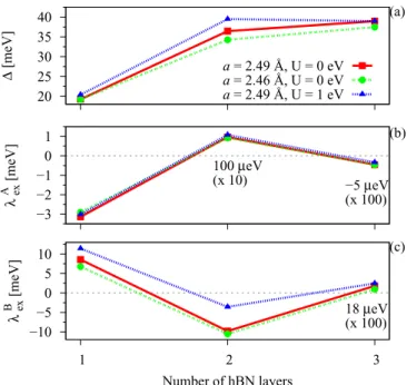
(a) Dependence on the number of hBN layers. Figure 5 shows the dependence of the proximity gap and the two exchange parametersλAexandλBexon the number of hBN layers between Co and graphene. We can see that the exchange parameters change sign after an additional insulating layer is added. The proximity gapnearly doubles for two layers of hBN and stays essentially unchanged when a third layer is added since the local environment of graphene does not change anymore. The parameters obtained with the minimal proximity exchange model are summarized in Table II for a=2.489 ˚A and Hubbard U=0. For four layers of hBN, again, the parameters change sign, but they are even smaller than for three layers of hBN and thus are not included here.
The parametersλAexandλBexare already in theμeV regime for three hBN layers, which is a result of the strong barrier. The two-layer case is special for the case ofλBexsince this exchange parameter has a magnitude similar to that of the single-layer case due to the strong hybridization with thed orbitals close to the K point. We note that the distances for the three-layer case are similar to those for the two-layer case. We only have one additional distance between the two hBN layers directly below graphene, which was relaxed todhBN/hBN=3.088 ˚A.
As we have already seen, the bands of hBN are also spin split. To get the magnitude of the exchange splitting of the individual hBN layers, we look at the graphene/hBN/Co structure with three layers of hBN. In the band structure we
20 25 30 35 40
Δ [meV]
(a)
a = 2.49 Å, U = 0 eV a = 2.46 Å, U = 0 eV a = 2.49 Å, U = 1 eV
−3
−2
−1 0 1
λA ex [meV]
(b) 100 μeV
(x 10) −5 μeV
(x 100)
−10
−5 0 5 10
1 2 3
λB ex [meV]
Number of hBN layers
(c)
18 μeV (x 100)
FIG. 5. Influence of the number of hBN layers on the proximity- induced parameters for the graphene/hBN/Co structure, using thepz
model at the K point. Dependence of (a) the proximity gap, (b) the exchange parametersλAex, and (c)λBex on the number of hBN layers for different lattice constants or an additional Hubbard parameter of U=1.0 eV. Parameter values for two (three) layers of hBN were increased by a factor of 10 (100) for better visualization, as indicated.
can identify the highest- (lowest-) lying valence (conduction) bands, which are spin split, of the three individual layers, like in Fig.2(a). From that, we extract the band splittings of conductionEcondand valenceEvalbands of the individual hBN layers at the K point. The spin-up bands of hBN are always lying lower in energy than the spin-down ones at the K point. Due to the spin splitting of the bands, hBN can additionally act as a spin filter for tunneling electrons, as reported in Ref. [39]. In Fig. 6 we show the valence- and conduction-band splittings at the K point of the three hBN layers. We find that the exchange splitting of the first hBN layer (closest to the Co surface) is roughly 0.5 eV. The splittings of the second and third layers are exponentially suppressed, but
1 10 100 1000
1 2 3
ΔE [meV]
hBN layer
ΔEcond ΔEval
FIG. 6. ConductionEcondand valenceEvalband splittings of the three individual hBN layers at the K point. Values are obtained by identifying the spin-split hBN conduction and valence bands of the three individual layers in the band structure of the graphene/hBN/Co heterostructure for three layers of hBN.
the third layer still exhibits proximity exchange of more than 1 meV (10 meV for the conduction band).
(b) Lattice-constant effects. Since we have artificially set the lattice constant for all the (well-lattice-matched) materials to be the same value, we now consider its effect on the proximity structure. We use the graphene constanta=2.46 ˚A by simply changing the in-plane lattice constant of the slab to this value without changing the vertical distances between the layers, which should be more favorable for the description of graphene dispersion. The results in this case do not deviate much from the case with our adopteda=2.489 ˚A, as can be seen in Fig.5, but the Fermi velocity fora=2.46 ˚A and one hBN layer isvF=0.827×10⁶m/s, corresponding to a larger nearest-neighbor hopping parameter oft=2.56 eV.
(c) Hubbard U. Since the exact position of thed bands is crucial to see the giant proximity exchange in the case of two hBN layers, we consider what happens when we apply a Hubbard U parameter to the calculation and shift the d- orbital levels. From recent studies of graphene on copper [49]
we know that the copper bands have to be shifted down in energy byU=1.0 eV to match the measured band structure from angle-resolved photoemission spectroscopy experiments.
From other DFT studies [72–76], mainly on metal oxides, it is not possible to get a unique value for U. Thus we apply U=1.0 eV as a generic representative. The results are shown in Fig.5. We can see that the parametersandλAexstay almost unchanged, as they are not affected by the strong coupling with d orbitals. However,λBex, representing the valence Dirac band splitting, is strongly affected, especially in the case of two hBN layers (it is not affected for three layers). By applying the HubbardU, we shift the band with energyEvin Fig.4down, away from the Dirac states, so the splitting at the K point decreases. The energetic position of thed bands with respect to the Dirac bands strongly influences the pure band splittings at the K point if the hybridization is large. In the absence of experimental guidance into the exact relative position ofd levels in our system, we can thus only predict the general trends and rough magnitudes for the valence proximity splitting. If the dbands are indeed close to the Dirac point, their influence will be giant, and one can expect ramifications in spin tunneling and spin injection.
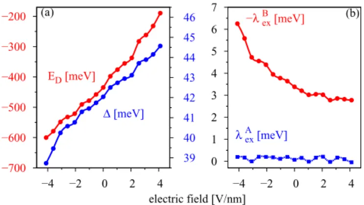
(d) Electric field effects. Figure 7 shows the influence of a transverse electric field on the proximity parameters , λAex, and λBex and the Dirac point energy ED for one layer of hBN. We model our electric field with a saw- like potential oriented perpendicular to the slab structure.
A positive field points from cobalt towards graphene and depletes its conduction electrons (lowers the magnitude ofED).
We can see thatEDandshow the same trend with electric field. In general, by increasing the electric field the doping level decreases; that is, one just shifts the Fermi level with respect to the Dirac bands. The proximity gapalso increases with increasing electric field, reflecting the charge transfer away from graphene. The continuous shift of the doping level with the applied electric field allows us to shift the Fermi level to the desired position. The general trend of the proximity parameters is that both tend to decrease with increasing electric field. For moderate field strengths of±2 V/nm, the parameters and thus the band splittings at the K point are almost unaffected.
−600
−550
−500
−450
−400
−350
−300
−250
−4 −2 0 2 4
17 18 19 20 21 22 23 24 (a) 25
ED [meV]
Δ [meV]
2 3 4 5 6 7 8 9 10
−4 −2 0 2 4
λBex [meV]
−λAex [meV]
(b)
electric field [V/nm]
FIG. 7. Influence of the electric field on the proximity-induced parameters for the graphene/hBN/Co structure for one hBN layer, using the minimalpzmodel at the K point. Dependence of the (a) Dirac energyED and the proximity gap and (b) the exchange parametersλAexandλBexon the applied transverse electric field.
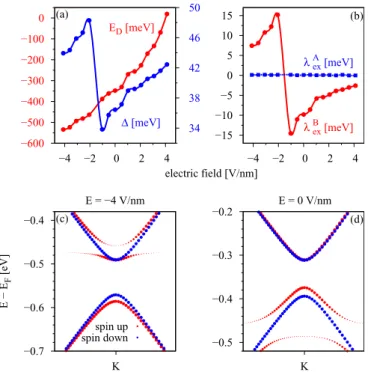
Most interesting is the two-hBN-layer case since here the valence-band splitting is strongly affected by hybridization with ad level. By applying an electric field, we can tune the energetic position of the Dirac point with respect to the d levels, which should also strongly affect the spin splitting of the graphene Dirac bands. In Fig.8we show the influence of
−600
−500
−400
−300
−200
−100 0
−4 −2 0 2 4 34 38 42 46 (a) 50
(c)
ED [meV]
Δ [meV]
−15
−10
−5 0 5 10 15
−4 −2 0 2 4 λBex [meV]
λAex [meV]
(b)
(d) electric field [V/nm]
−0.7
−0.6
−0.5
−0.4
K E − EF [eV]
E = −4 V/nm
spin up
spin down −0.5
−0.4
−0.3
−0.2
K E = 0 V/nm
FIG. 8. Influence of the electric field on the proximity-induced parameters for the graphene/hBN/Co structure for two hBN layers, using the minimalpzmodel at the K point. Dependence of the (a) Dirac energyED and the proximity gap and (b) the exchange parametersλAex and λBex on the applied transverse electric field. (c) and (d) The calculated spin-resolved band structure projected on the graphene states in the vicinity of the Dirac point for two different field strengths, illustrating the reversal of the valence spin states at the K point.
the electric field on the proximity parameters for two layers of hBN.
We can see that the Dirac point energyEDincreases with electric field, as for the monolayer hBN case. The proximity parameterλAexstays constant in magnitude around 100μeV. In Figs.8(c)and8(d), we show the calculated spin-resolved band structure of the graphene/hBN/Co heterostructure for two hBN layers, projected on the graphene states in the vicinity of the Dirac point for different field strengths. The spin-up graphene valence band at the K point is lying lower in energy than the spin-down one for E= −4 V/nm and vice versa for E= 0 V/nm. Therefore the parameter λBex is positive (negative) for fields smaller (larger) than −1.5 V/nm [see Fig. 8(b)].
Thecrossoverhappens at about−1.5 V/nm. The reason for these reversing spin states is the resonantd level. At a certain energetic configuration between the Dirac point and the d level, adjusted by the external electric field, the hybridization of the d level with graphene valence pz states leads to the change of the sign of the spin splitting parameters. This allows us to control the sign of the injected spin by applying an electric field, shifting the Dirac bands through the resonant d level. (Of course, this effect can only be observed if thed bands are indeed close to the Dirac point. DFT calculations can provide, at most, indications of this occurring due to the insufficient treatment of correlations that are important for d orbitals of transition metals.) Also, the proximity gap jumps in magnitude at the same field strength, roughly−1.5 V/nm, since the parameters andλBex of the pz model are connected. Apart from the jump, the gap parameter increases with increasing field strength.
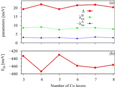
(e) Additional cobalt layers. Finally, we analyze the influ- ence of additional Co layers on the band structure (Fig. 9).
As we increase the number of Co layers, mored bands are introduced into the dispersion. Consequently, in the vicinity of the K point in Fig.2(a)graphene states can be disturbed by these additional Co bands.
−480
−460
−440
−420
3 4 5 6 7 8
ED [meV]
Number of Co layers 0
5 10 15 20
parameters [meV]
(a)
(b) Δ
λBex
−λAex
FIG. 9. Influence of the number of Co layers on the band structure for the graphene/hBN/Co system for one hBN layer, using the minimalpz model at the K point. Dependence of (a) the proximity gapand the exchange parametersλAex andλBex, as well as (b) the Dirac energyED, on the number of Co layers.
We can see that the band splittings of the graphene Dirac states at the K point do not get influenced much by additional layers since the parametersλAexandλBexstay almost constant, but the Dirac energy, which is our measure for the doping level, saturates only after six Co layers are present. We conclude that three Co layers suffice to obtain representative proximity parameters, and six Co layers are needed to fix the relative positioning of the bands.
B. Graphene/hBN/nickel 1. Structure
We now use Ni as the ferromagnet like in the approach with Co. Nickel crystallizes in a fcc lattice and has a magnetic moment of about 0.6μB, smaller than the one for hcp cobalt, which is 1.7μB[77]. Thus we expect the effects of proximity- induced magnetism to be smaller for the Ni substrate. In order to stack a hexagonal lattice on top of it, we need to consider the (111) plane. The lattice constant of Ni [77] isa=3.524 ˚A, and thus the lattice constant of the quasihexagonal lattice of the (111) plane is12√
2a=2.492 ˚A. As a result, the (111) plane of Ni is suitable for making heterostructures with graphene; the lattice mismatch is small. We fix an effective average lattice constant ofa=2.48 ˚A for the systems with Ni. In this case, the lowest-energy configuration is when nitrogen atoms are at the top sites above Ni and boron atoms are at fcc sites above Ni. Carbon atoms sit on top of boron atoms and at the hollow sites, above the center of a hexagonal ring of hBN (see Fig.10), in agreement with previous DFT studies [46,64,65].
After relaxation of atomic positions we obtained layer distances of dNi/hBN=2.105 ˚A between Ni and hBN and dhBN/Gr=3.015 ˚A between hBN and graphene (measured
Nickel Nitrogen
Boron Carbon
~ 2.1 Å
~ 3.0 Å
~ 0.1 Å
(a) (b)
top fcchcp (1)
(2) (3)
CB CA
a ~ 2.48 Å
FIG. 10. Structure of graphene/hBN/Ni, with labels for the differ- ent atoms. (a) Top view of the structure, with one unit cell emphasized by the dashed line. (b) Side view with stacking configuration: CBis over boron, and CA is over the hBN ring. Nitrogen is at the top site above Ni, and boron is above the fcc site of Ni. The indicated distances are measured between graphene/Ni and the nitrogen atom of hBN since the hBN layer is slightly corrugated byz=0.101 ˚A, with the boron atom closer to the Ni surface. Numbers in parentheses indicate the Ni layer.
−0.8
−0.6
−0.4
−0.2
K
E − EF[eV] pz(CA)
pz(CB)
dz2(3), pz(N) dz2
(a) (b)
(c) Eu
Ev Ew
spin up spin down
−150
−100
−50 0 50 100 150
25 20 15 10 5 0 5 10 15 20 25
E − E0[meV] (cond)
(val) Model
DFT
0 6 12 18
15 10 5 0 5 10 15
E [meV]
k [10−3/Å]
(val) (cond) M
( )
top fcchcp (1)
(2) (3)
CB CA
NB
Ni
d (1/2)
(2)
FIG. 11. Spin-polarized band structure of the graphene/hBN/Ni heterostructures for one layer of hBN. (a) Band structure in the vicinity of the Dirac point with labels for the main orbital contributions. LabelsEj,j=u, v, w, are the energy bands, which correspond to the Nid states used to fit thepz-dmodel Hamiltonian in Eq. (5). (b) The fit to thepz-dmodel with a side view of the structure. First-principles data (dotted lines) are well reproduced by the model (solid lines). (c) The corresponding splittings of the valence (val) and conduction (cond) Dirac states of graphene. The fit parameters areE0= −527.98 meV, ˜=22.98 meV, ˜λAex= −1.25 meV, ˜λBex=8.17 meV,Eu= −272.58 meV, Ev= −201.27 meV,Ew= −158.17 meV, vB↑=10.15 meV, wB↓=4.19 meV. The Fermi velocity to match the slope away from the K point is vF=0.81×10⁶m/s. The fit parameters are again obtained in the same way as for the Co case.
between C/Ni and N atoms, respectively, since the hBN layer is corrugated).
The layer distances of this minimum-energy configuration are in agreement with Refs. [46,65,66], which reportdhBN/Gr= 3.22–3.40 ˚A and dNi/hBN=1.96–2.12 ˚A. Again, the hBN- layer is not flat anymore but slightly corrugated by 0.101 ˚A, in agreement with Refs. [65,67]. For hBN we use an AA stacking (B over N, N over B), which is the energetically favorable one, with distances between the layers in the range ofdhBN/hBN=2.99–3.08 ˚A (details are given in Secs.IV B 3 andIV B 4).
2. One hBN layer
Figure 11(a) shows the calculated spin-polarized band structure of the graphene/hBN/Ni heterostructure for one layer of hBN. The graphene Dirac states for spin up are lying lower in energy than the spin-down ones, as in the Co case. Comparing Ni and Co, we notice that the Dirac point energyEDfor Ni is about 100 meV lower than for Co, but the proximity-induced band splittings are smaller, as expected due to the smaller magnetic moment of Ni. In general the band structures are quite similar, with the difference being that Nid states do not influence the Dirac states as much as Co does. Additionally, we notice that the spin-up d bands are formed by the same orbitals as for Co, while the spin-down d band near the K point is formed by different orbitals [mixture ofd orbitals of Ni layers (1/2) exceptdz2] due to the different lattices of Ni and Co. Most of all, we notice that there is nodband crossing the conduction Dirac states in the relevant energy andkregion.
The fit to thepz-dmodel is shown by solid lines to the DFT data in Fig.11(b). We see that thepz-d model Hamiltonian,
Eq. (5), describes our first-principles results very well with the fit parameters given in TableI. Like in the Co case, the gap in the dispersion is roughly 40 meV, and the band splittings are of the order of 10 meV. We additionally employ our minimal model to extract the effective band spin splittings (see TableII).
Due to the weak hybridization withd orbitals, the minimal model parameters are very close to the parameters of thepz-d model.
3. Two hBN layers
Figure 12 shows the calculated band structure and the fit to the pz-d model in the case of two layers of hBN and three layers of Ni. Again, the positions of carbon CA
did not change with respect to the hBN layers, while the position of CB changed to be on top of the uppermost boron atom. The layer distance between the two hBN layers was relaxed todhBN/hBN =2.995 ˚A, and the distance between the uppermost hBN layer and graphene wasdhBN/Gr=3.110 ˚A in the two-layer case. The corrugation of the lower hBN layer and the distance between hBN and Ni did not change. The inset in Fig. 12(b) shows the geometry for two layers of hBN. Figure12(a)shows the spin-polarized band structure of graphene/hBN/Ni for two layers of hBN. The spin-up graphene Dirac states are again no longer lying lower in energy than the spin-down ones, leading to the reversal of the sign of the exchange parameters, just as for Co. The fit parameters for the pz-d model are given in TableI. The fit to thepz-d model is shown in Fig.12(b).
We can see that the band splittings for both the conduction and valence Dirac states are smaller than in the single-hBN- layer case, as expected due to the additional insulating layer,