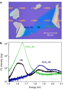
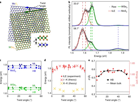
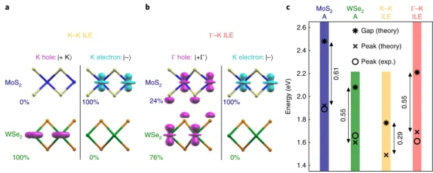
• Keine Ergebnisse gefunden

Momentum-space indirect interlayer excitons in transition-metal dichalcogenide van der Waals heterostructures

N/A
N/A
Protected

Academic year: 2021

Aktie "Momentum-space indirect interlayer excitons in transition-metal dichalcogenide van der Waals heterostructures"

Copied!
6
0
0

Wird geladen.... (Jetzt Volltext ansehen)

Volltext

(1)

1

Theoretical Chemistry, Department of Chemistry and Food Chemistry, TU Dresden, Dresden, Germany.

2

Institut für Experimentelle und Angewandte Physik, Universität Regensburg, Regensburg, Germany.

3

Departamento de Fisica, Universidade Federal do Ceara, Fortaleza, Ceara, Brazil.

4

Department of Chemistry, Columbia University, New York, NY, USA.

5

National University of Science and Technology, MISIS, Moscow, Russia.

6

These authors contributed equally: Jens Kunstmann, Fabian Mooshammer. *e-mail: jens.kunstmann@tu-dresden.de; tobias.korn@physik.uni-regensburg.de

Monolayers of transition-metal dichalcogenides feature exceptional optical properties that are dominated by tightly bound electron–hole pairs, called excitons. Creating van der Waals heterostructures by deterministically stacking indi- vidual monolayers can tune various properties via the choice of materials

1

and the relative orientation of the layers

2,3

. In these structures, a new type of exciton emerges where the electron and hole are spatially separated into different layers.

These interlayer excitons

4–6

allow exploration of many-body quantum phenomena

7,8

and are ideally suited for valleytronic applications

9

. A basic model of a fully spatially separated electron and hole stemming from the K valleys of the mono- layer Brillouin zones is usually applied to describe such exci- tons. Here, we combine photoluminescence spectroscopy and first-principles calculations to expand the concept of inter- layer excitons. We identify a partially charge-separated elec- tron–hole pair in MoS

2

/WSe

2

heterostructures where the hole resides at the Γ point and the electron is located in a K valley.

We control the emission energy of this new type of momen- tum-space indirect, yet strongly bound exciton by variation of the relative orientation of the layers. These findings represent a crucial step towards the understanding and control of exci- tonic effects in van der Waals heterostructures and devices.

An optical micrograph of a representative MoS

2

/WSe

2

heterobi- layer, which was fabricated by deterministic transfer and stacking

10

followed by an annealing procedure, is shown in Fig. 1a. All het- erobilayer and isolated regions of the constituent monolayers were thoroughly studied by micro-photoluminescence spectroscopy, and typical spectra are shown in Fig. 1b. The monolayer regions display the well-known A exciton and trion peaks

11–14

near 1.65 and 1.9 eV for WSe

2

(green) and MoS

2

(blue), respectively. In the heterobilayer region the same two peaks are discernible, but they are slightly shifted in energy due to the modified dielectric environment

15,16

. However, in addition, a new peak near 1.6 eV is observed, which is absent in the monolayer regions. We assign this peak to the inter- layer exciton (ILE)

4,17

.

Now, we control the relative orientation of the transition-metal dichalcogenide (TMD) layers to reveal the k-space indirect nature of this ILE in MoS

2

/WSe

2

heterobilayers. The twist angle is mea- sured with respect to the zigzag direction of each layer (green and

blue arrows in Fig. 2a), varying between 0° (aligned) and 60° (anti- aligned). A total of 15 heterobilayers with twist angles covering this range were fabricated, and the ILE emission was observable as a high-intensity photoluminescence peak in all samples. The twist angle was determined by second-harmonic generation (SHG) mea- surements and the samples were further characterized by Raman spectroscopy (for details, see Supplementary Information). The presence of the ILE becomes more obvious in Fig. 2b, which dis- plays photoluminescence spectra from the heterobilayer region of two samples with twist angles of 33.0° and 58.7° and their decom- position into three Gaussian peaks. The comparison of the two pan- els shows that as the twist angle is varied, the ILE peak displays a greater energy shift than the A exciton or trion peaks. As is clear from Fig. 2c, the latter do not exhibit a distinct dependence on the twist angle. Figure 2d shows that the ILE energy (red circles) shifts as a continuous function of the twist angle over a range of 50 meV.

The maximum of the curve is near 30° and it exhibits a slight asym- metry (that is, the minimum near 0° has a smaller energy than the minimum near 60°). Similar twist-angle-dependent, slightly asym- metric shifts of photoluminescence peaks have been observed in twisted bilayer MoS

2

(refs

2,3,18

).

We are able to explain this effect quantitatively via density functional theory (DFT) calculations. Details can be found in the Supplementary Information. An analysis of the geometries revealed that the mean layer separation of a heterobilayer changes as a continuous function of the twist angle over a range of 0.07 Å, as shown in Fig. 2e. This result can be ascribed to steric effects since the surface of a TMD monolayer is not atomically smooth but corrugated due to protrusion of the chalcogen atoms out of the metal-atom plane. For angles near 0° or 60°, Fig. 2e indicates a reduction of the mean layer separation by 1%. In these systems, long-wavelength moiré patterns are formed and the individual layers maximize their adhesion by adopting static spatial fluctua- tions. To study the consequences of these observations, we now analyse the electronic structure of the MoS

2

/WSe

2

heterobilayer (for details, see Supplementary Information). A level-alignment diagram is shown in Fig. 3a. It illustrates the staggered band align- ment of the heterobilayer, the optical transitions in the two mono- layers that give rise to the A excitons (vertical arrows) and the K− K and Γ − K interlayer transitions. Due to the generally weak

Momentum-space indirect interlayer excitons in transition-metal dichalcogenide van der Waals heterostructures

Jens Kunstmann    1,6 *, Fabian Mooshammer 2,6 , Philipp Nagler 2 , Andrey Chaves 3,4 , Frederick Stein 1 ,

Nicola Paradiso 2 , Gerd Plechinger 2 , Christoph Strunk 2 , Christian Schüller 2 , Gotthard Seifert 1,5 ,

David R. Reichman 4 and Tobias Korn 2 *

(2)

coupling between the monolayers in TMD heterostructures, the Bloch wavevectors defining the K valleys of the monolayers are also approximately good quantum numbers of the heterobilayer.

In Fig. 2d, K− K and Γ − K interlayer transition energies of twisted heterobilayers, as obtained from DFT calculations, are plotted as a function of twist angle. To allow a visual comparison of the DFT transition energies with the photoluminescence ILE energies, the DFT values in Fig. 2d are rigidly shifted by 0.445 eV, which implies that (relative) energy differences and not absolute energies are compared. The comparison reveals a remarkable quantitative correspondence with the Γ − K transition (red) but not with K− K (yellow). This suggests that the ILE is related to the Γ − K transi- tion. For the monolayer A type transitions, the DFT results exhibit no change with twist angle (see Supplementary Information).

The behaviour exposed by the DFT calculations is in full agree- ment with the photoluminescence results of Fig. 2d, because the change of the Γ − K transition energy is essentially a shift of the Γ point valence band energy (white arrow in Fig. 3a), an effect that should be well captured by DFT (for details, see Supplementary Section 3.2.4)

18,19

.

To better understand the impact of the layer separation on the electronic structure of the MoS

2

/WSe

2

heterobilayer, we studied by DFT an artificial model system that is anti-aligned and lattice-com- mensurate by applying strain. We considered 28 different transi- tions between valence and conduction band extrema and calculated their energies as a function of layer separation (see Supplementary Information). Most transitions exhibit either no dependence on the layer separation or a linear dependence with a negative slope (including K− K). There is only a single transition, Γ − K, that lies within a reasonable energy range, and has the correct trend and a positive slope of 0.47 eV Å

−1

, in excellent agreement with 0.44 eV Å

−1

found for realistic systems in Fig. 2e. These results uniquely identify

the observed ILE to be related to the Γ − K transition and not to K− K that is usually assumed when studying ILEs. Additional evidence supporting this key finding of our work is provided by analysing the twist angle and temperature dependencies of the ILE photolumines- cence intensity and by an exciton model.

We note that if the ILE was related to a K− K transition, its pho- toluminescence emission should be observable only for nearly (anti-)aligned structures because the transition probability of k-space direct transitions is higher (Fig. 3b)

20

. However, the analy- sis of the photoluminescence intensity as a function of twist angle in the heterobilayers shows no pronounced angle-dependence (see Supplementary Information).

For indirect optical transitions, the difference between the wavevectors of the electron and holes states is compensated by coupling to a phonon and the efficiency of this process can be partially tuned by varying the temperature, which controls the phonon population. Temperature-dependent photolumines- cence measurements of a heterobilayer and isolated WSe

2

and MoS

2

monolayers are shown in Fig. 3c. We observe a systematic blueshift of all exciton peaks with decreasing temperature. We also observe a complex behaviour of the relative photolumines- cence intensities in the heterobilayer region. The ILE photolumi- nescence, which is the most prominent emission peak at room temperature, decreases relative to the MoS

2

intralayer emission as the temperature decreases. This further supports the iden- tification of the transition as being indirect in k-space and is in stark contrast to the supposed K− K transition observed in WSe

2

/ MoSe

2

heterobilayers

5,20,21

, for which the ILE photoluminescence yield monotonically increases with decreasing temperature

22,23

. We also observe that the WSe

2

intralayer emission is quenched with decreasing temperature, as reported previously for WSe

2

monolayers

24,25

. Additional measurements and discussion of the temperature-dependent photoluminescence are presented in the Supplementary Information.

We now analyse the localization of electron and hole wavefunc- tions in the MoS

2

/WSe

2

heterobilayer. Figure 4a,b shows partial charge densities of electron and hole states for the K− K and Γ − K transitions in the model system calculated with DFT. Three unique states are involved, the K-valley electron state |− 〉 , the K-valley hole state |+ K〉 and the Γ -valley hole state |+ Γ 〉 . The electron–hole wavefunction overlap of an ILE can be quantified by projecting the hole state |+ k〉 (k = Γ or K) onto the MoS

2

layer o

k

= |〈 MoS

2

|+ k〉 |

2

. The overlap of the K− K transition (see Fig. 4a) is nearly zero (o

K

≈ 0%) because electrons and holes involve only transition-metal atom d-states and reside 6.6 Å apart (see Fig. 2e). The photolumi- nescence intensity scales with the square of the transition matrix element, which suggests that radiative recombination of K− K ILE is suppressed and is thus not seen in our photoluminescence mea- surements

26

. This is very different for the Γ − K transition (Fig. 4b):

|+ Γ 〉 is strongly affected by interlayer hybridization and therefore extends over both layers with Mo, S, W and Se atoms all participat- ing. It has a large component that resides in the MoS

2

monolayer (o

Γ

= 24%) where |− 〉 is localized. Therefore, the matrix element is much larger for Γ − K transitions than it is for K− K ones.

Our observations strongly imply the picture of an ILE with high photoluminescence intensity that does not represent the thermo- dynamically lowest-energy states (that is, the K− K excitonic transi- tion), and is fully consistent with transitions of the Γ − K type. We note that our system is pumped with a sufficiently high energy to create carriers across a wide range of momenta with a hot, non- thermal distribution. Thus, the observed response will depend intimately on the non-equilibrium kinetics of exciton formation and recombination, as well as charge transfer

27

and a host of non- radiative relaxation channels

28,29

. However, it should be noted that non-equilibrium effects alone are insufficient to explain why the Γ − K ILE seems to be so strongly favoured. One possibility is that

50 μ m

1.5 1.6 1.7 1.8 1.9 2.0 2.1

10

1

10

2

10

3

10

4

HB MoS

2

ML

PL intensity (log)

Energy (eV)

a

b

WSe

2

ML

WSe

2

ML MoS

2

ML HB

Fig. 1 | interlayer excitons in MoS

2

/WSe

2

heterobilayers. a, An optical

micrograph of a sample with a twist angle of 58.7

°

, fabricated by

deterministic transfer and stacking. Monolayer (ML) and heterobilayer

(HB) regions are indicated. b, Photoluminescence (PL) spectra of the

heterobilayer and monolayer regions. The occurrence of an interlayer

exciton near 1.6 eV is discernible in the heterobilayer.

(3)

1.5 1.6 1.7 1.8 1.9 58.7°

33.0°

Energy (eV)

PL intensity (normalized, shifted vertically)

Raw ILE

WSe

2

MoS

2

b a

0 20 40 60

1.6 1.7 1.8 1.9

MoS

2

ML HB

WSe

2

ML

HB Twist angle (°)

Energy (eV)

c

1.4 1.5 1.6

Energy (eV)

d

d (Å )

6.3 6.4 6.5 6.6 6.7

1.55 1.60 1.65

Energy (eV)

e

0 20 40 60

Twist angle (°)

0 20 40 60

Twist angle (°) Mean bulk

MoS

2

Twist

angle

WSe

2

d

ILE (experiment) Γ −K (theory) K−K (theory)

HB

Fig. 2 | Tuning the interlayer exciton energy via interlayer twist. a, An atomic structure illustration of a MoS

2

/WSe

2

heterobilayer. The twist angle is the relative lattice orientation of the two layers. Inset: side view of the heterobilayer; the layer separation d is the distance between the Mo and W planes.

b, Photoluminescence spectra and their decomposition into Gaussian peaks for two heterobilayers with twist angles of 33.0° and 58.7°. Besides the A exciton or trion peaks, arising from WSe

2

(green) and MoS

2

(blue), an ILE near 1.6 eV has emerged (red). The dashed vertical lines allow comparison of the peak positions; the black lines are the sum of the Gaussians. The extracted peak energies are used in c and d. c, A exciton or trion energies for monolayer and heterobilayer regions for varying twist angles. The dashed horizontal lines indicate the mean values. We observe no clear dependence on the twist angle but a redshift from the monolayer to the heterobilayer. d, ILE energies and calculated transition energies for heterobilayers with different twist angles. The error bars indicate the standard deviation of the ILE energy determined from spatial averaging of the ILE photoluminescence emission (see Supplementary Information). The Γ − K and K − K values are calculated with DFT and they are rigidly upshifted by 0.445 eV (see the text). Only the trend of Γ − K is in quantitative agreement with the experiment. e, The mean layer separation (indicated graphically in the inset of a) as a function of twist angle, as calculated with dispersion-corrected DFT. Steric repulsion of chalcogen atoms, due to lattice mismatch and incommensurability, creates a twist angle dependence and leads to bigger layer separations than the mean of the layer spacings of bulk MoS

2

and WSe

2

samples (dashed horizontal line). The red dots correspond to ‘ILE (experiment)’ in d. A strong correlation is discernible; the linear proportionality factor is 0.44 eV Å

−1

.

a

Twist

angle k

x

k

y

K Γ

Γ K

1.6 2.0 1.6 2.0

1.6 1.8

PL intensity (normalized, shifted vertically)

Energy (eV)

Mo S

2

WS e

2

Hybrid

E K

K

K

K Γ

∣ +K 〉

|– 〉

∣ + Γ〉

K–K A Γ –K EE (eV)

F

A

–2 –1 0 1

2 WSe

2

ML MoS

2

ML

1.8 1.8

Energy (eV) Energy (eV)

b c HB

T

A ILEA T

T

90 K 150 K 180 K 240 K 295 K

Fig. 3 | electronic structure of MoS

2

/WSe

2

heterobilayers. a, Band alignment diagram. The valence band maximum at the Γ valley |+ Γ 〉 is a hybrid state of both layers and it moves up as hybridization increases. The coloured vertical arrows indicate monolayer transitions. Γ − K and K − K are possible interlayer transitions. b, The two-dimensional band structure of the heterobilayer near the band edges. In twisted heterobilayers, the Brillouin zones of MoS

2

(blue) and WSe

2

(green) are misaligned. Therefore, both heterobilayer transitions, K − K and Γ − K, are k-space indirect (the wavevectors of the electron and holes states differ). However, for twist angles near 0° (aligned) or 60° (anti-aligned), K− K is k-space direct (no wavevector difference).

c, Temperature-dependent photoluminescence spectra measured on isolated WSe

2

(left panel) and MoS

2

(right panel) monolayers and on a heterobilayer region (centre panel). Every spectrum is individually normalized to the peak of highest intensity. In the heterobilayer region, spatial averaging of

photoluminescence spectra is performed due to the spatially inhomogeneous ILE emission (see Supplementary Information for details). The dotted lines

trace the spectral evolution of the WSe

2

and MoS

2

A exciton and trion, as well as the ILE as a function of temperature. As the temperature is decreased,

the ILE photoluminescence, which is the most prominent emission at room temperature, is suppressed compared to the intralayer MoS

2

emission in the

heterobilayer region. This finding supports our assertion that the ILE is related to a k-space indirect, phonon-assisted transition.

(4)

the large, real-space overlap of electron and holes in the respective layers kinetically favours the formation and recombination of par- tially charge-separated Γ − K excitons despite the fact that such states are not formed from band-edge carriers.

The large, real-space overlap of these k-space indirect ILEs sug- gests a binding energy that is increased as compared to their K− K counterparts that are fully charge-separated. Therefore, we calcu- late the exciton binding energies Δ E

X

of the A excitons as well as K− K and Γ − K ILEs using the quantum electrostatic heterostruc- ture model

30

and a variational wavefunction ansatz. Excitonic inter- layer interactions are described within a tight-binding approach (see Supplementary Information for details). Experimentally, the exciton binding energy is defined as Δ = E X E gap qpE gap opt , where E gap qp is the quasiparticle bandgap and E gap opt is the optical gap, measured as the photoluminescence peak energy. The results of these calcu- lations are given in Fig. 4c, where Δ E

X

is indicated by arrows. For the A excitons, the theoretical and experimental energies agree well. Δ E

X

values are of the order of 0.5 eV, in good agreement with previous results

31

. For the K− K ILE, Δ E

X

= 0.29 eV, which is also in agreement with earlier results

15,32

. For Γ − K, we obtain a much bigger value of 0.55 eV, comparable to those of A excitons. The main reason for this large number is the delocalization of the hole state over both layers that enhances the electron–hole Coulomb attraction and gives the Γ − K ILE also a strong monolayer char- acter in MoS

2

. We note that the ILE emission energy calculated using this large binding energy is in good agreement with the experimentally observed value. It should also be noted that charge separation creates excitons with an interlayer dipole moment of μ

IL

= (1 − o

k

)ed ≈ (1 − o

k

) × 1.4 Debye (e is the elementary charge and d is the layer separation). Its magnitude is reduced by inter- layer hybridization since o

K

< o

Γ

. Thus K− K and Γ − K excitons can potentially be distinguished by measuring μ

IL

.

Methods

Methods, including statements of data availability and any asso- ciated accession codes and references, are available at https://doi.

org/10.1038/s41567-018-0123-y.

Received: 16 July 2017; Accepted: 21 March 2018;

Published online: 30 April 2018

References

1. Geim, A. K. & Grigorieva, I. V. Van der Waals heterostructures. Nature 499, 419–425 (2013).

2. van der Zande, A. M. et al. Tailoring the electronic structure in bilayer molybdenum disulfide via interlayer twist. Nano Lett. 14, 3869–3875 (2014).

3. Liu, K. et al. Evolution of interlayer coupling in twisted molybdenum disulfide bilayers. Nat. Commun. 5, 4966 (2014).

4. Fang, H. et al. Strong interlayer coupling in van der Waals heterostructures built from single-layer chalcogenides. Proc. Natl Acad. Sci. USA 111, 6198–6202 (2014).

5. Rivera, P. et al. Observation of long-lived interlayer excitons in monolayer MoSe

2

–WSe

2

heterostructures. Nat. Commun. 6, 6242 (2015).

6. Rivera, P. et al. Valley-polarized exciton dynamics in a 2D semiconductor heterostructure. Science 351, 688–691 (2016).

7. Snoke, D. Spontaneous Bose coherence of excitons and polaritons. Science 298, 1368–1372 (2002).

8. Fogler, M. M., Butov, L. V. & Novoselov, K. S. High-temperature superfluidity with indirect excitons in van der Waals heterostructures. Nat. Commun. 5, 4555 (2014).

9. Xu, X., Yao, W., Xiao, D. & Heinz, T. F. Spin and pseudospins in layered transition metal dichalcogenides. Nat. Phys. 10, 343–350 (2014).

10. Castellanos-Gomez, A. et al. Deterministic transfer of two-dimensional materials by all-dry viscoelastic stamping. 2D Mater. 1, 011002 (2014).

11. Splendiani, A. et al. Emerging photoluminescence in monolayer MoS

2

. Nano Lett. 10, 1271–1275 (2010).

12. Mak, K. F. et al. Atomically thin MoS

2

a new direct-gap semiconductor.

Phys. Rev. Lett. 105, 136805 (2010).

13. Zhao, W. et al. Evolution of electronic structure in atomically thin sheets of WS

2

and WSe

2

. ACS Nano 7, 791–797 (2013).

14. Mak, K. F. et al. Tightly bound trions in monolayer MoS

2

. Nat. Mater. 12, 207–211 (2013).

15. Latini, S., Winther, K. T., Olsen, T. & Thygesen, K. S. Interlayer excitons and band alignment in MoS

2

/hBN/WSe

2

van der Waals heterostructures.

Nano Lett. 17, 938–945 (2017).

16. Raja, A. et al. Coulomb engineering of the bandgap and excitons in two-dimensional materials. Nat. Commun. 8, 15251 (2017).

17. Chiu, M.-H. et al. Spectroscopic signatures for interlayer coupling in MoS

2

–WSe

2

van der Waals stacking. ACS Nano 8, 9649–9656 (2014).

18. Yeh, P.-C. et al. Direct measurement of the tunable electronic structure of bilayer MoS

2

by interlayer twist. Nano Lett. 16, 953–959 (2016).

19. Zhu, X., Fahy, S. & Louie, S. G. Ab initio calculation of pressure coefficients of band gaps of silicon: Comparison of the local-density approximation and quasiparticle results. Phys. Rev. B 39, 7840–7847 (1989).

20. Nayak, P. K. et al. Probing evolution of twist-angle-dependent interlayer excitons in MoSe

2

/WSe

2

van der Waals heterostructures. ACS Nano 11, 4041–4050 (2017).

21. Nagler, P. et al. Interlayer exciton dynamics in a dichalcogenide monolayer heterostructure. 2D Mater. 4, 025112 (2017).

22. Miller, B. Long-lived direct and indirect interlayer excitons in van der Waals heterostructures. Nano Lett. 17, 5229–5237 (2017).

100%

0%

24%

76%

100%

0%

K–K ILE

0%

100%

K hole:∣+ K〉 K electron:∣–〉

1.4 1.6 1.8 2.0 2.2 2.4 2.6

Peak (exp.) Peak (theory) Gap (theory) MoS

2

A

WSe

2

A

K–K ILE Γ –K

ILE

MoS

2

WSe

2

MoS

2

WSe

2

Γ hole: ∣+Γ〉 K electron:∣–〉

Γ –K ILE

Energy (eV)

a b c

0.61 0.55 0.29 0.55

Fig. 4 | The nature of interlayer excitons. a, The hole | + K 〉 and electron | − 〉 states of the K − K ILE are localized in the individual layers (the pink and magenta contours are partial charge densities). b, Hole and electron states of the Γ − K ILE. While the electron state |− 〉 is localized only in the MoS

2

layer, the hybrid hole |+ Γ 〉 state is delocalized over both layers. The percentages correspond to the fraction of the wavefunction that is localized in each layer.

c, Comparison between experimental (circles) and theoretical (crosses) photoluminescence peak energies for different monolayer A excitons and ILE. The

arrows indicate exciton binding energies Δ E

X

, as calculated with our model. The theoretical bandgaps (asterisks) are G

0

W

0

results from the literature

31

. The

theoretical results closely match the experimental data. Δ E

X

for the Γ − K ILE is comparable to values in the monolayer, and the resulting emission energy is

in good agreement with the experimentally observed ILE peak.

(5)

23. Hanbicki, A. T. et al. Double indirect interlayer exciton in a MoSe

2

/WSe

2

van der Waals heterostructure. Preprint at https://arxiv.org/abs/1802.05310 (2018).

24. Zhang, X.-X., You, Y., Zhao, S. Y. F. & Heinz, T. F. Experimental evidence for dark excitons in monolayer WSe

2

. Phys. Rev. Lett. 115, 257403 (2015).

25. Arora, A. et al. Excitonic resonances in thin films of WSe

2

: from monolayer to bulk material. Nanoscale 7, 10421–10429 (2015).

26. Kira, M., Jahnke, F. & Koch, S. W. Microscopic theory of excitonic signatures in semiconductor photoluminescence. Phys. Rev. Lett. 81, 3263–3266 (1998).

27. Hong, X. et al. Ultrafast charge transfer in atomically thin MoS

2

/WS

2

heterostructures. Nat. Nanotech. 9, 682–686 (2014).

28. Sun, D. et al. Observation of rapid exciton–exciton annihilation in monolayer molybdenum disulfide. Nano Lett. 14, 5625–5629 (2014).

29. Steinleitner, P. et al. Direct observation of ultrafast exciton formation in a monolayer of WSe

2

. Nano Lett. 17, 1455–1460 (2017).

30. Andersen, K., Latini, S. & Thygesen, K. S. Dielectric genome of van der Waals heterostructures. Nano Lett. 15, 4616–4621 (2015).

31. Rasmussen, F. A. & Thygesen, K. S. Computational 2D materials database:

electronic structure of transition-metal dichalcogenides and oxides. J. Phys.

Chem. C 119, 13169–13183 (2015).

32. Wilson, N. R. et al. Determination of band offsets, hybridization, and exciton binding in 2D semiconductor heterostructures. Sci. Adv. 3, e1601832 (2017).

Acknowledgements

The work is financially supported by the German Research Foundation (DFG) under grant numbers SE 651/45-1, GRK 1570, KO 3612/1-1 and KO 3612/3-1. G.S. gratefully

acknowledges financial support by the Ministry of Education and Science of the Russian Federation (grant no. K3-2017-064). Computational resources for this project were provided by ZIH Dresden.

Author contributions

F.M., P.N., C. Schüller and T.K. conceived the experiments. F.M. fabricated the samples and performed the optical spectroscopy and data analysis together with P.N., G.P. and T.K. N.P. and C. Strunk annealed samples and performed AFM measurements. J.K.

performed the DFT calculations together with F.S. and G.S., interpreted the results and supervised the theoretical analysis. A.C. carried out the exciton modelling under the supervision of D.R.R. using parameters provided by J.K. J.K. D.R.R. and T.K. wrote the paper together with F.M. and P.N. All authors discussed the results.

Competing interests

The authors declare no competing interests.

Additional information

Supplementary information is available for this paper at https://doi.org/10.1038/

s41567-018-0123-y.

Reprints and permissions information is available at www.nature.com/reprints.

Correspondence and requests for materials should be addressed to J.K. or T.K.

Publisher’s note: Springer Nature remains neutral with regard to jurisdictional claims in

published maps and institutional affiliations.

(6)

Methods

Sample fabrication. Heterobilayer samples were fabricated by means of a deterministic transfer process

10

. For this, we initially exfoliated MoS

2

and WSe

2

flakes from bulk crystals (here, we utilized a natural MoS

2

crystal and a synthetic WSe

2

crystal bought at HQgraphene.com) onto polydimethylsiloxane substrates.

Monolayer regions of these flakes were identified via optical microscopy. Then, we first transferred a MoS

2

flake onto the target substrate, a silicon wafer piece covered with a SiO

2

layer and pre-defined metal markers. Subsequently, the WSe

2

flake was transferred on top of the MoS

2

. For each of the heterobilayers fabricated in this way, the relative orientation of the individual layers was chosen to optimize the overlap region of the monolayer parts of the flakes. Subsequent to the transfer, the heterobilayers were annealed. For this, they were mounted in a furnace, which was initially flushed with a H

2

/Ar gas mixture and then pumped to high vacuum. In vacuum, the samples were annealed at a temperature of 150 °C for 5 h.

Optical spectroscopy. Photoluminescence and Raman measurements were performed in a self-built microscope set-up (details are published elsewhere

33

).

A continuous-wave laser (wavelength 532 nm) was coupled to a × 100 microscope objective and focused to a submicrometre spot on the sample surface.

Photoluminescence and scattered light were collected with the same objective, passed through long-pass filters, coupled into a grating spectrometer and detected with a Peltier-cooled CCD (charge-coupled device). For temperature-dependent photoluminescence measurements, the sample was mounted on the cold finger of a small He-flow cryostat. For photoluminescence mapping, the sample was moved beneath the fixed microscope objective using a motorized xy stage, and photoluminescence spectra were collected for sample positions defined on a square lattice. To extract information from these spectra, an automated fitting routine was employed, which yields the integrated intensity, spectral position and full- width at half-maximum for each spectral feature extracted using a Gaussian fit function. SHG measurements were performed in a similar, self-built microscope set-up, which was optimized to yield high SHG throughput. Here, a Ti:sapphire laser oscillator (pulse length 100 fs, central wavelength 815 nm) was used as an excitation source. The laser light coupled into the microscope objective was linearly polarized, and the same polarizer was used to analyse the reflected light, so that only the signal polarized parallel to the excitation was detected. To separate the SHG signal from the reflected fundamental laser wavelength, a dichroic mirror and short-pass filters were employed before the SHG signal was either coupled into a grating spectrometer to be detected by a CCD, or focused onto an avalanche photodiode. In the measurements using the avalanche photodiode, a lock-in scheme was employed to further increase the signal-to-noise ratio. For SHG mapping, the sample was moved beneath the fixed microscope objective using a motorized xy stage. For polarization-dependent measurements, the combined polarizer/analyser was rotated using a motorized stage.

Experimental data analysis. For each heterobilayer structure, a

photoluminescence map was measured at room temperature. To compensate for the spatial inhomogeneity of the ILE emission, spatial averaging was employed.

For this, the average photoluminescence emission energy of the ILE, and its

standard deviation, were calculated from the values extracted from an automated fitting routine applied to individual photoluminescence spectra collected in the heterobilayer region where sufficiently intense ILE photoluminescence was observed. The size of these regions varied from sample to sample, but, on average, more than 60 spectra were evaluated for an individual heterobilayer.

DFT calculations. The DFT calculations were carried out with the Perdew–Burke–

Ernzerhof functional

34

and the Tkatchenko–Scheffler dispersion-interaction- correction scheme

35

using the projector augmented wave method

36

and a plane- wave basis set with a cutoff energy of 259 eV, as implemented in VASP (Vienna Ab initio Simulation Package)

37,38

. For the k-point sampling, an in-plane sampling density of 0.1 Å

2

was used. It was carefully checked that this density leads to converged total energies (energy differences are smaller than 1 meV per atom).

The k-space integration was carried out with a Gaussian smearing method using an energy width of 0.05 eV for all calculations. All unit cells were built with at least 10 Å separation between replicates in the perpendicular direction to achieve negligible interaction. All systems were fully structurally optimized until all interatomic forces and stresses on the unit cell were below 0.01 eV Å

−1

and 10 kbar, respectively. Spin–orbit interactions were generally not taken into account and the inclusion of these interactions does not alter any of our conclusions as spin–orbit- dependent interlayer interactions in TMDs have not been reported before

2,18

. The wavefunction overlap o

k

= |〈 MoS

2

|+ k〉 |

2

is calculated by integrating the partial charge density of the state |+ k〉 (k = Γ or K) over the half of the volume of the unit cell that contains the MoS

2

layer. The cutting plane between the two halves is the minimum of the plane-averaged line charge density in the van der Waals gap between the layers.

Data availability. The data that support the plots within this paper and other findings of this study are available from the corresponding authors upon reasonable request.

References

33. Plechinger, G. et al. Optical spectroscopy of interlayer coupling in artificially stacked MoS

2

layers. 2D Mater. 2, 034016 (2015).

34. Perdew, J. P., Burke, K. & Ernzerhof, M. Generalized gradient approximation made simple. Phys. Rev. Lett. 77, 3865–3868 (1996).

35. Tkatchenko, A. & Scheffler, M. Accurate molecular van der Waals interactions from ground-state electron density and free-atom reference data. Phys. Rev.

Lett. 102, 073005 (2009).

36. Blöchl, P. E. Projector augmented-wave method. Phys. Rev. B 50, 17953–17979 (1994).

37. Kresse, G. & Furthmüller, J. Efficiency of ab-initio total energy calculations for metals and semiconductors using a plane-wave basis set. Comput. Mater.

Sci. 6, 15–50 (1996).

38. Kresse, G. & Furthmüller, J. Efficient iterative schemes for ab initio

total-energy calculations using a plane-wave basis set. Phys. Rev. B 54,

11169–11186 (1996).

Abbildung

Fig. 1 | interlayer excitons in MoS 2 /WSe 2  heterobilayers. a, An optical  micrograph of a sample with a twist angle of 58.7 ° , fabricated by  deterministic transfer and stacking
Fig. 2 | Tuning the interlayer exciton energy via interlayer twist. a, An atomic structure illustration of a MoS 2 /WSe 2  heterobilayer
Fig. 4 | The nature of interlayer excitons. a, The hole | +  K 〉   and electron | − 〉   states of the K −  K ILE are localized in the individual layers (the pink and  magenta contours are partial charge densities)

Referenzen

ÄHNLICHE DOKUMENTE

Here, we report on an alternative approach to realize an extremely broadband cw fluorescence light source, which is based on a fiber with multiple-doped cores pumped by a single

Herr Meister scheint zu spüren, daß sich auf unserer Seite eine Irritation ausbreitet, und macht folgendes Angebot: &#34;Vielleicht sag ich Ihnen mal ganz kurz was über meine

In the present contribution, I illustrate by means of describing the initial sequences of a theme-centred interview including the events in the interview- relationship, as well as

In table 2 three data sets are given: one concerning the routine method in the participating laboratories, one concerning the Hertz 9 technique and one concerning the direct

CTD, Rosette, salinities Ocean Physics John Love Marie Robert Cruise Psychology University of Szczecin Anna Flak O2, reversing thermometers Ocean Physics Bernard Minkley

Our repeat hydrography section continues to be a joint program with Canadian JGOFS. A CTD survey along Line PR6 was completed. DMS was analyzed in sea water at the same stations to

The present investigation was undertaken with the aim of studying the behaviour of the 420 K glow peak in deformed NaCl: TI phosphors as a function of

We consider an impurity driven mixing of the Kramers doublet and in section 3.1 an admixture mechanism where the electron spin relaxes due to either a piezoelectric phonon or