Magnetotransport in heterostructures of transition metal dichalcogenides and graphene
Tobias Völkl,1Tobias Rockinger,1Martin Drienovsky,1Kenji Watanabe,2Takashi Taniguchi,2 Dieter Weiss,1and Jonathan Eroms1,*
1Institut für Experimentelle und Angewandte Physik, Universität Regensburg, 93040 Regensburg, Germany
2NIMS, 1-1 Namiki, Tsukuba, Ibaraki 305-0044, Japan
(Received 14 June 2017; revised manuscript received 28 July 2017; published 6 September 2017) We use a van der Waals pickup technique to fabricate different heterostructures containing WSe2(WS2) and graphene. The heterostructures were structured by plasma etching, contacted by one-dimensional edge contacts, and a top gate was deposited. For graphene/WSe2/SiO2samples we observe mobilities of∼12 000 cm2V−1s−1. Magnetic-field-dependent resistance measurements on these samples show a peak in the conductivity at low magnetic fields. This dip is attributed to the weak antilocalization (WAL) effect, stemming from spin-orbit coupling. Samples where graphene is encapsulated between WSe2(WS2) and hexagonal boron nitride show a much higher mobility of up to∼120 000 cm2V−1s−1. However, in these samples no WAL peak can be observed.
We attribute this to a transition from the diffusive to the quasiballistic regime. At low magnetic fields a resistance peak appears, which we ascribe to a size effect due to boundary scattering. Shubnikov–de Haas oscillations in fully encapsulated samples show all integer filling factors due to complete lifting of the spin and valley degeneracies.
DOI:10.1103/PhysRevB.96.125405
I. INTRODUCTION
In recent years, the assembly of van der Waals heterostruc- tures containing graphene has gained much attention [1]. En- capsulating graphene between hexagonal boron nitride (hBN) and employing one-dimensional edge contacts [2] have proven to be reliable methods to fabricate high mobility devices.
With this, a number of effects, such as ballistic transport [3], viscous electron flow [4], and moiré patterns [5], have been observed. However, employing other two-dimensional (2D) materials for encapsulation allows to further tailor the properties of graphene. One promising objective is to increase the spin-orbit coupling (SOC) in graphene as this may offer numerous possibilities, including the generation of a pure spin current through the spin-Hall effect or the manipulation of spin currents through an electric field. Bringing graphene into the proximity of transition metal dichalcogenides (TMDCs) has been predicted theoretically [6,7] and observed experimentally [8–11] to increase SOC in graphene. Furthermore, transport measurements [12] and recent Raman measurements indicate the suitability of these substrates for high mobility graphene [13]. This is in contrast to previously explored methods for increasing SOC in graphene, such as hydrogenation [14,15], fluorination [16], or the attachment of heavy atoms [17,18], as these methods have the disadvantage of increas- ing the scattering and therefore decreasing the mobility of graphene.
Here, we report on a comparison of magnetotransport in graphene/TMDC heterostructures in a broad mobility range, realized by different material combinations in the van der Waals stacked layer sequence. We integrate one-dimensional contacts into the TMDC/graphene processing scheme achiev- ing a high yield of functional devices and include top gates using a TMDC layer as a gate dielectric. In diffusive samples,
*jonathan.eroms@ur.de
we observe weak antilocalization and study proximity-induced spin-orbit interaction at different out-of-plane electric fields, whereas in high mobility samples, a ballistic size effect and the quantum-Hall effect are observed.
II. SAMPLE FABRICATION
Heterostructures were fabricated by using a dry pickup process [2]. Three different types of devices were fabricated.
For device type 1 [see Fig.1(a)] monolayer graphene was picked up by exfoliated multilayer WSe2 and placed onto a standard p++-doped Si/SiO2 chip. For device type 2 monolayer graphene was encapsulated between hBN and WS2, whereas for device type 3 [see Fig.1(b)] bilayer graphene was encapsulated between hBN and WSe2. After assembly all three devices were annealed for 1 h at 320◦C in vacuum and 1 h at 320◦C in forming gas. Annealing removes contaminations between the layers as well as the remaining poly propylene carbonate on top of the WSe2(WS2) flake. Then electron-beam lithography and reactive ion etching with CHF3/O2 were employed to define a Hall-bar structure. The graphene then was contacted by 5-nm Cr/80-nm Au side contacts. These edge contacts showed high reliability as 70 of 74 contacts were functional. As a last step 10-nm Al2O3 were deposited by atomic layer deposition, followed by a Au top gate. The Al2O3 layer is necessary to prevent any leakage between the top gate and the graphene at the sides of the stack.
III. EXPERIMENTAL RESULTS A. Diffusive Regime
For measurements in the diffusive regime monolayer graphene/WSe2 is placed onto SiO2 in device type 1. We therefore observe a mobility of onlyμ=12 000 cm2V−1s−1 atT =1.65 K. Figure2depicts the magnetoconductivity of this sample at different temperatures. In order to suppress universal conductance fluctuations an average over 15 curves at
FIG. 1. (a) and (b) Schematic cross section of the devices.
(a) Cross section of device type 1, consisting of monolayer graphene and WSe2 on top of SiO2. (b) Cross section of device type 3.
Bilayer graphene is encapsulated between hBN and WSe2. (c) Optical microscope picture of device 3. Part of the hBN/graphene stack lies on a WSe2flake; the other part lies directly on the SiO2substrate.
slightly different backgate voltages with a mean charge-carrier concentration ofn=1.0×10¹²/cm2 was taken. The curves were obtained in a four-point lock-in measurement with an ac current of Iac=10 nA for the curves at T =1.65 and T =4.2 K, Iac=50 nA at T =10 K and Iac=100 nA at T =100 K at a frequency off =13 Hz.
The occurrence of a sharp peak in the magnetoconductivity can be explained by weak antilocalization, stemming from spin-orbit coupling. For the case where the intervalley scatter- ing rate exceeds the decoherence rate, the low-magnetic-field dependence of the conductivity correction due to WAL can be described as [19]
σ(B)= − e2 2π h
F
τB−1 τφ−1
−F
τB−1 τφ−1+2τasy−1
−2F
τB−1 τφ−1+τso−1
, (1)
-0.010 -0.005 0.000 0.005 0.010
-0.2 -0.1 0.0 0.1 0.2 0.3
0.4 T=1.65K
T=4.2K T=10K T=20K
Δσ(e2 /h)
Bz(T)
FIG. 2. Gate averaged magnetoconductivity of a graphene/WSe2 sample at different temperatures. The peak intensity decreases with increasing temperature as the phase coherence length decreases. The data were fitted by Eq. (1) (red curves).
-0.010 -0.005 0.000 0.005 0.010
0.0 0.1 0.2 0.3 0.4 0.5
-15 -10 -5 0 5
1 10
2 1 0 -1 -2
τ(ps)
Utg(V)
Ubg(V) Ubg=5V, Utg=-2V
Ubg=-5V, Utg=0V Ubg=-15V, Utg=2V
Δσ(e2 /h)
Bz(T)
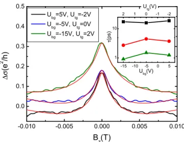
FIG. 3. Gate averaged magnetoconductivity at three different top- and backgate voltage combinations. The top- and backgate voltages are chosen in a way that leaves the charge-carrier concentration unchanged while a transverse electric field is applied. The curves are fitted by Eq. (1) (red curves). The inset: Electric-field dependence ofτφ(black squares),τso(green triangles), andτasy(red circles).
where F(x)=ln(x)+(1/2+1/x) with (x) being the digamma function,τB−1=4DeB/¯h, τφis the phase coherence time,τsois the spin-orbit scattering time, andτasyis a scattering time that takes into account only spin-orbit coupling that is asymmetric in thez→ −zdirection. Here τso combines symmetric and antisymmetric spin-orbit scatterings: τso−1 = τsym−1 +τasy−1[19].
Fitting the curve in Fig. 2 at T =1.65 K (red curves in Fig. 2) gives τφ =25.7, τso=0.57, and τasy=1.71 ps.
These are comparable to the values that were reported for graphene placed on WSe2 [9] and WS2 [8–10].τso, which is an upper bound for the spin-relaxation time is therefore much shorter than the values typically found in pristine graphene (100 ps–1 ns) [20–22]. The occurrence of WAL with such small τsois therefore a clear indication of strong SOC in this device.
With increasing temperature the feature in Fig.2decreases as the phase coherence timeτφdecreases, and the peak disappears atT =20 K.
The dual gated device allows us to examine the WAL peak with an applied transverse electric field while leaving the charge-carrier density unchanged. Figure 3 shows the magnetoconductivity at three different top- and backgate voltage combinations. Applying the electric field strongly decreasesτsofromτso =1.5 toτso =0.91 ps in one direction of the electric field andτso=1.25 ps in the other direction.
The SOC strength is expected to increase with an electric field due to the Rashba effect [23]. However, τso depends on the total out-of-plane electric field acting on the carriers, which is composed of the externally applied field as well as an internal field due to the WSe2-graphene interface. The weak asymmetry in the external electric field therefore points to a small contribution of an internal field. This is in contrast to the findings of Yanget al., in graphene/WS2 samples, who reported a linear dependence of the spin-orbit scattering rate τasy with the applied electric field, whereas they assume the symmetric part of the scattering rate to be zero [10].
-2 0 2 4 6 8 10 12 14 16 0
20 40 60 80 100 120 140
160 T=1.4K
Bz(T) R xx(Ω)
0 500 1000 1500 2000
ν=28ν=
24 ν=ν=2019ν=17
ν=15 ν=13
ν=30ν=26ν=22ν=18
R xy(Ω)
ν=14 ν=16
FIG. 4. Shubnikov–de Haas oscillations (black curve) and quantum-Hall effect (blue curve) in hBN/graphene/WS2. The split- ting of valley and spin degeneracies in the Landau levels indicates a high mobility of the sample.
Spin relaxation is expected to be dominated by the Dyakonov-Perel mechanism. The SOC strengthDP can be estimated by [24]
τso−1=4τe(DP/h)¯ 2. (2) This results in a SOC strength ofDP=0.7–1.0 meV, which agrees well with theoretical predictions [7]. For the case of Elliot-Yafet dominated spin relaxation the SOC strength can be estimated by [24]τso−1=τe−12EY/EF2. This results in an unrealistically large SOC strength ofEY=35–65 meV.
Furthermore, we observe a decrease in τso with increasing charge-carrier concentration, which indicates that spin relax- ation is dominated by the Dyakonov-Perel mechanism.
B. Ballistic Regime
In order to increase the mobility of graphene we have encapsulated graphene between WSe2(WS2) and hBN [see Fig.1(b)]. Figure4shows the Shubnikov–de Haas oscillations (black curve) and the quantum-Hall effect (blue curve) of de- vice 2, containing monolayer graphene between hBN and WS2. This device showed mobilities ofμ=50 000 cm2V−1s−1on the hole side and μ=120 000 cm2V−1s−1 on the electron side. In Fig.4, a lifting of the spin and valley degeneracies can be observed, which results in integer filling factors in addition to the expected values of 4n+2 for monolayer graphene.
This behavior is typical for high mobility graphene [25]. The resistance peak at low magnetic fields, followed by a negative magnetoresistance behavior, will be discussed later.
In order to directly compare the substrates WSe2and SiO2
in device 3, a bilayer graphene/hBN stack was placed in such a way that part of the stack lies on a WSe2 flake and part of it lies directly on the SiO2 substrate [see Fig. 1(c)].
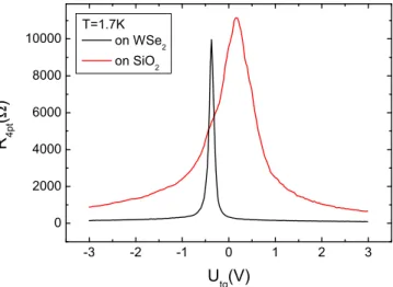
Figure5 shows top-gate sweeps of the four-point resistance of these two areas at T =1.7 K. From this we extract a mobility of μ=3200 cm2V−1s−1 on the hole side and μ=5300 cm2V−1s−1 on the electron side for the graphene on SiO2. For the graphene on WSe2 we extract μ=57 000 andμ=92 000 cm2V−1s−1for hole and electron sides. The overall high mobilities resulting from encapsulation confirm
-3 -2 -1 0 1 2 3
0 2000 4000 6000 8000 10000
R 4pt(Ω)
Utg(V)
T=1.7K on WSe2 on SiO2
FIG. 5. Top-gate sweeps of the sample depicted in Fig.1(c). The black curves shows the resistance of the sample region lying on WSe2, whereas the red curve depicts the resistance of the sample region on SiO2.
the suitability of WS2and WSe2as substrates for high mobility graphene.
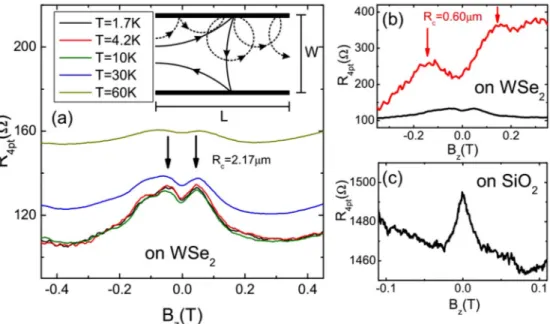
Figure6(c)shows the magnetoresistance of the graphene on the SiO2substrate. Here we observe a peak in the resistance around B =0 T, which we ascribe to weak localization.
Fitting this peak with the formula for weak localization in bilayer graphene [26] reveals a phase coherence length ofLφ ∼ 490 nm and an intervalley scattering length ofLi∼420 nm.
For the part of the bilayer graphene on WSe2 we observe a dip in the resistance aroundB =0 T in Fig.6(a). At first glance this feature might be interpreted as WAL. However, this dip is much too large (σ =20e2/h) and too broad to be fitted with Eq. (1). Furthermore, the temperature dependence is much weaker, and the dip is still visible atT =60 K, in contrast to the WAL feature in Fig. 2. Figure 6(b) shows the magnetoresistance of two bilayer graphene samples with different widths. Although the black curve shows the magne- toresistance of the sample from Figs.5and6(a), with a width of W =4μm, the red curve shows the magnetoresistance of a sample with width W =1.5μm. The mobility of this sample was μ=90 000 cm2V−1s−1 on the hole side and μ=100 000 cm2V−1s−1on the electron side. This behavior, i.e., the resistance peak at finiteB, we ascribe to a ballistic effect, stemming from diffusive boundary scattering [27–29].
A schematic of this effect is shown in the inset of Fig.6(a). At low magnetic fields the scattering between boundaries, and, therefore, the overall resistance, is initially increased [solid lines in the inset of Fig.6(a)]. When the cyclotron diameter becomes smaller than the sample width, the scattering be- tween boundaries is suppressed, and therefore the resistance decreases [dashed lines in the inset of Fig.6(a)]. From the curves in Fig.6(b), the cyclotron radiusRcat the magnetic field where the resistance reaches the maximum can be calculated as
Rc(B)= hk¯ F
eBmax = h¯√ π n
eBmax. (3)
The calculated cyclotron radii are Rc=2.17μm for the sample with width W =4μm and Rc=0.60μm for the
FIG. 6. (a) Magnetoresistance of hBN/graphene/WSe2at different temperatures. The inset: Schematic electron trajectories forRC> W (solid lines) andRC < W(dashed lines). (b) Magnetoresistance for two samples with different widths. The feature aroundB=0 T is more pronounced and broader for a sample with widthW=1μm (red line) than for a sample with widthW=4μm (black line). This indicates that this feature is caused by a size effect due to boundary scattering. Furthermore, a linear background can be observed on the red curve.
(c) Magnetoresistance of the sample area on SiO2shows weak localization behavior.
sample with widthW =1μm. This shows thatRcscales with the sample widthW. For semiconductor 2D electron gases, a relation W=0.55Rc was found [28], whereas for hBN encapsulated graphene a different prefactor was observed [29]. The resistance peak at the low magnetic field in Fig.4 also is attributed to this effect.
No WAL behavior could be observed for graphene encap- sulated between hBN and WSe2(WS2). We attribute this to a transition from the diffusive to the quasiballistic regime.
Since Eq. (1) was developed in the diffusive regime, it is only valid for the case ofτφ > τasy> τso> τe. Due to the higher mobility for devices of types 2 and 3, we findτeto be in the range ofτe≈1 ps. Therefore the relationτso > τemay not be valid here. We expect WAL to be suppressed due to reduced backscattering and the WAL peak to be narrower, resulting from the higher mobility in these samples (a similar behavior has been observed in GaAs heterostructures [30]). Therefore the absence of WAL in these samples is not indicative of a lower SOC strength.
IV. CONCLUSION
In conclusion we investigated charge transport in several graphene/WSe2(WS2) heterostructures. We successfully
employed the established fabrication techniques for hBN/graphene/hBN stacks to heterostructures containing WSe2(WS2) and graphene. Placing a graphene/WSe2 stack on SiO2resulted in a mobility ofμ=12 000 cm2V−1s−1. In this sample we observed a peak in the magnetoconductivity, which we attributed to the WAL effect, stemming from SOC.
Applying an electric field increased the SOC strength in this sample. Encapsulating graphene between WSe2(WS2) and hBN increased the mobility to up toμ=120 000 cm2V−1s−1. No WAL behavior could be observed in these samples. We attribute this to a transition from the diffusive to the quasibal- listic regime. This is confirmed further by the occurrence of a quasiballistic size effect due to diffusive boundary scattering.
These results confirm the suitability of WSe2(WS2) as a substrate for high quality graphene with strongly increased SOC.
ACKNOWLEDGMENTS
Financial support by the Deutsche Forschungsgemeinschaft (DFG) within the Programs No. GRK 1570 and No. SFB 689 is gratefully acknowledged. The authors would like to thank J. Fabian and T. Korn for fruitful discussions.
[1] A. K. Geim and I. V. Grigorieva, Nature (London)499, 419 (2013).
[2] L. Wang, I. Meric, P. Y. Huang, Q. Gao, Y. Gao, H. Tran, T.
Taniguchi, K. Watanabe, L. M. Campos, D. A. Muller, J. Guo, P. Kim, J. Hone, K. L. Shepard, and C. R. Dean,Science342, 614(2013).
[3] T. Taychatanapat, K. Watanabe, T. Taniguchi, and P. Jarillo- Herrero,Nat. Phys.9,225(2013).
[4] D. A. Bandurin, I. Torre, R. K. Kumar, M. Ben Shalom, A.
Tomadin, A. Principi, G. H. Auton, E. Khestanova, K. S.
Novoselov, I. V. Grigorieva, L. A. Ponomarenko, A. K. Geim, and M. Polini,Science351,1055(2016).
[5] C. R. Dean, L. Wang, P. Maher, C. Forsythe, F. Ghahari, Y. Gao, J. Katoch, M. Ishigami, P. Moon, M. Koshino, T. Taniguchi, K.
Watanabe, K. L. Shepard, J. Hone, and P. Kim,Nature (London) 497,598(2013).
[6] T. P. Kaloni, L. Kou, T. Frauenheim, and U. Schwingenschlögl, Appl. Phys. Lett.105,233112(2014).
[7] M. Gmitra, D. Kochan, P. Högl, and J. Fabian,Phys. Rev. B93, 155104(2016).
[8] Z. Wang, D.-K. Ki, H. Chen, H. Berger, A. H. MacDonald, and A. F. Morpurgo,Nat. Commun.6,8339(2015).
[9] Z. Wang, D.-K. Ki, J. Y. Khoo, D. Mauro, H. Berger, L. S.
Levitov, and A. F. Morpurgo,Phys. Rev. X6,041020(2016).
[10] B. Yang, M.-F. Tu, J. Kim, Y. Wu, H. Wang, J. Alicea, R. Wu, M. Bockrath, and J. Shi,2D Mater.3,031012(2016).
[11] A. Avsar, J. Y. Tan, T. Taychatanapat, J. Balakrishnan, G. K. W.
Koon, Y. Yeo, J. Lahiri, A. Carvalho, A. S. Rodin, E. C. T.
O’Farrell, G. Eda, A. H. C. Neto, and B. Özyilmaz, Nat.
Commun.5,4875(2014).
[12] A. V. Kretinin, Y. Cao, J. S. Tu, G. L. Yu, R. Jalil, K. S.
Novoselov, S. J. Haigh, A. Gholinia, A. Mishchenko, M. Lozada, T. Georgiou, C. R. Woods, F. Withers, P. Blake, G. Eda, A.
Wirsig, C. Hucho, K. Watanabe, T. Taniguchi, A. K. Geim, and R. V. Gorbachev,Nano Lett.14,3270(2014).
[13] L. Banszerus, H. Janssen, M. Otto, A. Epping, T. Taniguchi, K. Watanabe, B. Beschoten, D. Neumaier, and C. Stampfer, 2D Mater.4,025030(2017).
[14] A. H. C. Neto and F. Guinea, Phys. Rev. Lett.103, 026804 (2009).
[15] J. Balakrishnan, G. K. W. Koon, M. Jaiswal, A. H. C. Neto, and B. Özyilmaz,Nat. Phys.9,284(2013).
[16] A. Avsar, J. H. Lee, G. K. W. Koon, and B. Özyilmaz,2D Mater.
2,044009(2015).
[17] D. Ma, Z. Li, and Z. Yang,Carbon50,297(2012).
[18] J. Balakrishnan, G. K. W. Koon, A. Avsar, Y. Ho, J. H. Lee, M. Jaiswal, S.-J. Baeck, J.-H. Ahn, A. Ferreira, M. A. Cazalilla, A. H. C. Neto, and B. Özyilmaz,Nat. Commun.5,4748(2014).
[19] E. McCann and V. I. Fal’ko,Phys. Rev. Lett.108,166606(2012).
[20] N. Tombros, C. Jozsa, M. Popinciuc, H. T. Jonkman, and B. J.
van Wees,Nature (London)448,571(2007).
[21] W. Han, K. Pi, K. M. McCreary, Y. Li, J. J. I. Wong, A. G.
Swartz, and R. K. Kawakami, Phys. Rev. Lett. 105, 167202 (2010).
[22] F. Volmer, M. Drögeler, E. Maynicke, N. von den Driesch, M. L.
Boschen, G. Güntherodt, and B. Beschoten,Phys. Rev. B88, 161405(2013).
[23] Y. A. Bychkov and E. I. Rashba,J. Phys. C: Solid State Phys.
17,6039(1984).
[24] D. Huertas-Hernando, F. Guinea, and A. Brataas,Phys. Rev.
Lett.103,146801(2009).
[25] A. F. Young, C. R. Dean, L. Wang, H. Ren, P. Cadden-Zimansky, K. Watanabe, T. Taniguchi, J. Hone, K. L. Shepard, and P. Kim, Nat. Phys.8,550(2012).
[26] R. V. Gorbachev, F. V. Tikhonenko, A. S. Mayorov, D. W.
Horsell, and A. K. Savchenko, Phys. Rev. Lett. 98, 176805 (2007).
[27] C. Beenakker and H. van Houten, inSemiconductor Heterostruc- tures and Nanostructures, edited by H. Ehrenreich and D.
Turnbull, Solid State Physics Vol. 44 (Academic Press, San Diego, 1991), pp. 1–228.
[28] T. J. Thornton, M. L. Roukes, A. Scherer, and B. P. Van de Gaag, Phys. Rev. Lett.63,2128(1989).
[29] S. Masubuchi, K. Iguchi, T. Yamaguchi, M. Onuki, M. Arai, K.
Watanabe, T. Taniguchi, and T. Machida,Phys. Rev. Lett.109, 036601(2012).
[30] B. Grbi´c, R. Leturcq, T. Ihn, K. Ensslin, D. Reuter, and A. D.
Wieck,Phys. Rev. B77,125312(2008).