• Keine Ergebnisse gefunden

Strain-tunable orbital, spin-orbit, and optical properties of monolayer transition-metal dichalcogenides

N/A
N/A
Protected

Academic year: 2021

Aktie "Strain-tunable orbital, spin-orbit, and optical properties of monolayer transition-metal dichalcogenides"

Copied!
10
0
0

Wird geladen.... (Jetzt Volltext ansehen)

Volltext

(1)

Strain-tunable orbital, spin-orbit, and optical properties of monolayer transition-metal dichalcogenides

Klaus Zollner ,

*

Paulo E. Faria Junior, and Jaroslav Fabian

Institute for Theoretical Physics, University of Regensburg, 93040 Regensburg, Germany

(Received 24 September 2019; revised manuscript received 5 November 2019; published 15 November 2019) When considering transition-metal dichalcogenides (TMDCs) in van der Waals heterostructures for periodic ab initio calculations, usually, lattice mismatch is present, and the TMDC needs to be strained. In this study we provide a systematic assessment of biaxial strain effects on the orbital, spin-orbit, and optical properties of the monolayer TMDCs using ab initio calculations. We complement our analysis with a minimal tight-binding Hamiltonian that captures the low-energy bands of the TMDCs around the K and K

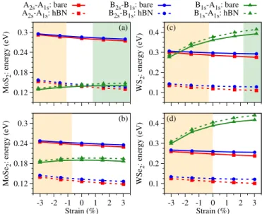
valleys. We find charac- teristic trends of the orbital and spin-orbit parameters as a function of the biaxial strain. Specifically, the orbital gap decreases linearly, while the valence (conduction) band spin splitting increases (decreases) nonlinearly in magnitude when the lattice constant increases. Furthermore, employing the Bethe-Salpeter equation and the extracted parameters, we show the evolution of several exciton peaks, with biaxial strain, on different dielectric surroundings, which are particularly useful for interpreting experiments studying strain-tunable optical spectra of TMDCs.

DOI: 10.1103/PhysRevB.100.195126

I. INTRODUCTION

A vastly evolving field of condensed-matter physics is that of two-dimensional (2D) van der Waals (vdW) materials and their hybrids. The available material repertoire covers semi- conductors [1–5] (MoS

2

, WSe

2

), ferromagnets [6–21] (CrI

3

, CrGeTe

3

), superconductors [22–24] (NbSe

2

), and topologi- cal insulators [25] (WTe

2

), which offer unforeseen potential for electronics and spintronics [26,27]. For example, mono- layer transition-metal dichalcogenides (TMDCs) are direct band gap semiconductors with remarkable physical properties [1–5,28–31], especially in the realm of optoelectronics [32], optospintronics [33–35], and valleytronics [36–38]. Currently, TMDCs, being stable in air, are a favorite platform for optical experiments, including optical spin injection due to helicity- selective optical excitations [39].

The ability to control and modify the electronic, spin, and optical properties of 2D materials is extremely valuable for investigating novel physical phenomena, as well as a potential knob for device applications. One possibility to do so in TMDCs is by deforming the crystal lattice via strain engi- neering [40–52]. Recent experiments have shown that strain modulation is very effective and can lead to changes in the optical transition energies by hundreds of meV with just a few percent of applied strain [40,41,44–47]. Even more interesting is that this strain modulation is completely reversible [44,45].

As a general trend observed in the experimental studies, bi- axial strain induces a significantly stronger modulation when compared to uniaxial strain, a fact also supported by ab initio calculations [53,54]. Furthermore, by strain engineering it is possible to localize excitons in specific regions, which is a

*

klaus.zollner@physik.uni-regensburg.de

viable approach to obtain spatially and spectrally isolated quantum emitters based on 2D materials [51,55–58].

Strain also plays an important role when TMDCs are stacked on or sandwiched by other 2D materials, creating vdW heterostructures [59,60]. An example of interesting physics present in vdW heterostructures is the proximity ef- fects [61]. Typical examples involving TMDCs are spin-orbit coupling (SOC) induced in graphene by TMDCs [33,62] and proximity exchange induced in the TMDC due to magnetic substrates [38,63–65].

Strain effects are extremely important from a theoretical point of view: By creating vdW heterostructures that fulfill the periodic boundary conditions of first-principles calcula- tions, it is often necessary to adjust the lattice parameters of the materials involved, therefore leading to strained crys- tals. Certainly, the strain—which is biaxial in first-principles calculations—will modify the electronic structure of the TMDC, and therefore, a systematic analysis of its behavior can provide valuable insight not only from an experimental point of view but also to aid in the design of novel heterostruc- tures.

In this paper, we study the effect of biaxial strain on the

orbital, spin-orbit, and optical properties of pristine mono-

layer TMDCs. We find that by tuning the lattice constant, the

orbital band gap and the spin splittings of the valence and

conduction bands drastically change. Specifically, the orbital

gap decreases linearly, while the valence (conduction) band

spin splitting increases (decreases) nonlinearly in magnitude,

when the lattice constant increases. The observed behavior

is universal for all studied TMDCs (MoS

2

, MoSe

2

, WS

2

,

WSe

2

). In addition, we show that spin splittings of the bands

result from an interplay of the atomic SOC values of the

transition-metal and chalcogen atoms. Finally, we analyze

the direct-indirect transition energies, and by employing the

(2)

Bethe-Salpeter equation we calculate the optical absorption spectra of the biaxially strained TMDC monolayers. We show the evolution of several exciton peaks and their energy dif- ferences as a function of strain, assuming different dielectric surroundings. We also extracted the gauge factors—the rates at which the exciton peak energies shift due to strain—which are relevant for comparison to experiments.

II. MODEL HAMILTONIAN

In this paper, we deal with TMDC monolayers. Therefore, we need a Hamiltonian that describes the low-energy bands of bare TMDCs around the K and K

valleys, including spin- valley locking. In Fig. 1 we show the orbital decomposed band structure of MoS

2

without inclusion of SOC as a rep- resentative example of a TMDC with general structure MX

2

(M for the transition-metal atom, X for the chalcogen atom).

The wave functions we use for the Hamiltonian are |

CB

=

| d

z2

and |

VBτ

=

12

( | d

x2y2

+ i τ | d

xy

), corresponding to the conduction band (CB) and valence band (VB) at K and K

since the band edges are formed by different d orbitals from the transition metal (see Fig. 1), in agreement with the literature [1]. The model Hamiltonian to describe the band structure (including SOC) of the TMDC close to K (τ = 1) and K

( τ = − 1) is

H = H

0

+ H

+ H

soc

, (1) H

0

= hv ¯

F

s

0

⊗ (τσ

x

k

x

+ σ

y

k

y

), (2)

H

=

2 s

0

σ

z

, (3)

H

soc

= τ s

z

⊗ (λ

c

σ

+

+ λ

v

σ

). (4) Here, v

F

is the Fermi velocity, and the Cartesian components k

x

and k

y

of the electron wave vector are measured from K (K

). The pseudospin Pauli matrices are σ

i

acting on the (CB, VB) subspace, and spin Pauli matrices are s

i

acting on

FIG. 1. Calculated orbital decomposed band structure of MoS

2

as a representative example of a TMDC. SOC is not included, and the different colors correspond to different orbitals or atoms.

the (↑, ↓) subspace, with i = {0, x, y, z}. For shorter notation we introduce σ

±

=

12

0

± σ

z

). TMDCs are semiconductors, and thus, H

introduces a gap, represented by parameter , in the band structure such that H

0

+ H

describes a gapped spectrum with spin-degenerate parabolic CB and VB. In addition the bands are spin split due to SOC, which is captured by the term H

soc

, with the parameters λ

c

and λ

v

describing the spin splitting of the CB and VB. The Hamiltonian H

0

+ H

+ H

soc

is already suitable to describe the spectrum of bare TMDCs around the band edges at K and K

. The four basis states are |

CB

, ↑, |

VBτ

, ↑, |

CB

, ↓, and |

VBτ

, ↓. From now on, we consider only first-principles results, where SOC is included.

III. GEOMETRY, BAND STRUCTURE, AND FITTED RESULTS

To study proximity effects in TMDCs, one has to interface them with other materials, for example, CrI

3

, to get proxim- ity exchange [63]. In these heterostructures, usually, lattice mismatch between the constituents is present, and we have to find a common unit cell for them to be applicable to periodic DFT calculations. The usual approach is to create supercells of the individual materials, such that they can form a common unit cell, and strain is minimized. Therefore, we introduce biaxial strain on the TMDC lattice, up to a reasonable limit, in heterostructure calculations. An important question is whether the biaxial strain will influence the intrinsic properties, such as orbital gap and spin-orbit splittings, of the TMDC. Therefore, we calculate the band structures of the monolayer TMDCs in a 1 × 1 unit cell for different lattice constants, corresponding to biaxial strain with a maximum of ±3%.

The electronic structure calculations and structural relax- ation of our geometries are performed with density func- tional theory (DFT) [66] using QUANTUM ESPRESSO [67].

Self-consistent calculations are performed with the k-point sampling of 30 × 30 × 1 for bare TMDC monolayers. We use an energy cutoff for charge density of 560 Ry, and the kinetic energy cutoff for wave functions is 70 Ry for the scalar relativistic pseudopotential with the projector augmented- wave method [68] with the Perdew-Burke-Ernzerhof (PBE) exchange correlation functional [69]. When SOC is included, the fully relativistic versions of the pseudopotentials are used.

In order to simulate quasi-2D systems, a vacuum of at least 16 Å is used to avoid interactions between periodic images in our slab geometries. Structural relaxations of the monolayers are performed with a quasi-Newton algorithm based on the trust radius procedure until all components of all forces are reduced below 10

4

[Ry/a

0

], where a

0

is the Bohr radius.

In Fig. 2 we show the geometry of a TMDC monolayer with general structure MX

2

, where M is the transition metal (Mo, W) and X is the chalcogen atom (S, Se). The distance between two chalcogen atoms is d

XX

, the distance between the transition-metal and the chalcogen atoms is d

MX

, and the distance between two transition-metal atoms is the lattice constant a. We consider a series of lattice constants close to the experimental and theoretically predicted values of each TMDC, as summarized in Table I.

The calculated band structure of MoS

2

including SOC is

shown in Fig. 3 as a representative example for all considered

(3)

FIG. 2. Geometry of a TMDC monolayer with general structure MX

2

, where M is the transition metal (Mo, W) and X is the chalco- gen atom (S, Se). (a) Side and (b) top views of the geometry, with labels for the lattice constant a, distance d

MX

(between the transition metal and the chalcogen atom), and d

XX

(between the two chalcogen atoms).

TMDCs. In agreement with previous calculations [1,2,73,74], we observe the spin valley coupling at the K and K

points. We are able to fit the Hamiltonian, H

0

+ H

+ H

soc

, to the low- energy bands of the TMDC at the K and K

valleys and obtain very good agreement with the calculated band structure, as can be seen in Figs. 3(b) and 3(c). The fit parameters for the different TMDCs are summarized in Table I, considering the equilibrium lattice constants obtained from first-principles lattice relaxation.

In order to analyze the dependence on the lattice con- stant, i.e., biaxial strain, we allow the chalcogen atoms to relax in their z position for every considered lattice constant.

Therefore, we do not change the symmetry, but naturally, the distances d

XX

and d

MX

will change as we apply biaxial strain.

TABLE I. Overview of the lattice parameters for all TMDCs, as well as fit parameters of the Hamiltonian H

0

+ H

+ H

soc

. The monolayer calculated lattice constant a (calc.), distances d

XX

, and d

MX

, as defined in Fig. 2. The orbital gap parameter , the Fermi velocity v

F

, and the SOC parameters λ

c

and λ

v

. The experimental lattice constants a (exp.) [70–72] of the bulk systems are given for comparison.

MoS

2

WS

2

MoSe

2

WSe

2

a (exp.) (Å ) 3.15 3.153 3.288 3.282

a (calc.) (Å ) 3.185 3.18 3.319 3.319

d

MX

(calc.) (Å ) 2.417 2.417 2.547 2.550

d

XX

(calc.) (Å ) 3.138 3.145 3.357 3.364

(eV) 1.687 1.812 1.461 1.525

v

F

(10

5 ms

) 5.338 6.735 4.597 5.948

λ

c

(meV) −1.41 15.72 −10.45 19.86

λ

v

(meV) 74.6 213.46 93.25 233.07

FIG. 3. (a) Calculated band structure of MoS

2

including SOC.

The color corresponds to the s

z

expectation value. (b) and (c) Calcu- lated low-energy CB and VB around the K point (symbols) with a fit to the model Hamiltonian (solid line).

We then calculate the low-energy band structure around the K and K

valleys and fit the model Hamiltonian H

0

+ H

+ H

soc

for a series of lattice constants. Due to time-reversal symmetry, it is enough to fit the Hamiltonian around the K point, taking into account the spin expectation values of the bands in order to find the correct signs of λ

c

and λ

v

. The three parameters , λ

c

, and λ

v

are fitted at the K point, where we have four DFT energies and three energy differences.

The remaining parameter, v

F

, is fitted around the K point to capture the curvature of the bands. The fitted parameters are thus free from correlations. In Fig. 4 we show the fit parameters obtained for MoS

2

as a function of the lattice constant. We find that the total energy E

tot

is minimized for the DFT-predicted lattice constant [1], which slightly deviates from the experimentally determined one for a bulk TMDC, also listed in Table I.

As we vary the lattice constant from smaller to larger values, the distance between two chalcogen atoms d

XX

gets smaller, while the distance between the transition-metal atom and the chalcogen atom d

MX

gets larger [see Fig. 4(c)].

The parameter , describing the orbital gap at the K and

K

valleys, decreases as we increase the lattice constant,

in agreement with the literature [48,54,75–78]. Keeping the

orbital-decomposed band structure (Fig. 1) in mind, the lattice

constant influences all atomic distances, the overlap of p

and d orbitals, and matrix elements in a tight-binding model

perspective [79,80]. Consequently, the energy of a given band

at a certain k point changes with the atomic distances. For

(4)

FIG. 4. Summary of the fit parameters for MoS

2

as a function of the lattice constant. (a) The gap parameter and the total energy E

tot

. The black data (SOC on M , X ) correspond to calculations where SOC is included for both atoms M and X , while for the red data (SOC on M), we turned off SOC on the X atoms. Dashed vertical lines indicate the equilibrium lattice constant. (b) The Fermi velocity v

F

. (c) The distances d

XX

and d

MX

. (d) and (e) The SOC parameters λ

c

and λ

v

. The difference (blue curve) is between the black and the red curves.

example, the CB (VB) edge at the K () point is formed by d

z2

orbitals and shifts down (up) in energy with increasing lattice constant (see animations in the Supplemental Material [81].

Note that for MoS

2

and strains of about − 1% ( + 1%), when we have a smaller (larger) lattice constant, the band gap becomes indirect [54,76,77] and is at KQ ( → K), where Q is the CB side valley along the K- line (see Fig. 1).

For the other TMDCs, the situation is similar, but for different strain amplitudes. Tuning the gap with uniaxial or biaxial strain consequently modifies the optical properties, such as the photolominescence spectrum, exciton-phonon coupling, and circular dichroism [46,82–84]. It has also been shown that strain applied to MoS

2

-based photodetectors can control the response time of the devices [49]. We address the effects of strain in the direct-indirect optical transitions in Sec. IV A and the role of excitonic effects in the direct gap regime in Sec. IV B.

The Fermi velocity v

F

, reflecting the effective mass, does not change drastically as we vary the lattice constant, but still we see some characteristic nonlinear behavior [see Fig. 4(b)].

The reason is that v

F

at [39], given by the effective hopping integral t between d

z2

and d

xy+x2y2

orbitals, mediated by chalcogen p orbitals, is influenced by atomic distances d

XX

and d

MX

. The most interesting are the SOC parameters λ

c

and λ

v

[see Figs. 4(d) and 4(e)]. Because we have two different atomic species in the unit cell, we consider the influence of the individual atoms, M and X , on the SOC parameters, which represent the spin splittings of the CB and VB. For that we

calculate the band structure once with SOC on both atom species and once artificially turning off SOC on the chalcogen atom by using a nonrelativistic pseudopotential for it. This allows us to resolve the contributions from the M and X atoms to the SOC parameters individually. The difference (blue curve) reflects the contribution from the chalcogen atoms to the splittings [see Figs. 4(d) and 4(e)].

We find that the parameter λ

c

decreases, while the pa- rameter λ

v

increases with increasing lattice constant. Both parameters depend in a nonlinear fashion on the biaxial strain.

At a certain lattice constant, the CB splitting in MoS

2

can even

make a transition through zero, reordering the two spin-split

bands in Fig. 3(b). In addition, the differences (blue curve) in

λ

c

and λ

v

decrease in magnitude, as we increase the lattice

constant. This we can understand from the fact that the spin

splittings of the CB and VB result from an interplay of the

atomic SOC values of the transition-metal and chalcogen

atoms, as derived from perturbation theory in Ref. [74]. We

confirm that the chalcogen atom has a negative contribution to

the CB splitting and a positive contribution to the VB splitting,

while the transition-metal atom gives positive contributions

to both splittings, in agreement with Ref. [74]. In Fig. 4 we

explicitly show how the spin splittings depend on the lattice

constant and how the different atom types contribute to it for

the case of MoS

2

. What is still missing so far is a microscopic

orbital-based description of how the spin splittings depend on

the lattice constant and respective distances, as, for example,

derived for graphene [85].

(5)

TABLE II. Fit parameters of the model Hamiltonian (1) for all four TMDCs and different values of biaxial strain. The lattice parameter a is given in Å, is given in eV, v

F

is given in 10

5

m / s, and λ

c

, λ

v

are given in meV.

MoS

2

MoSe

2

a v

F

λ

c

λ

v

a v

F

λ

c

λ

v

3.0854 2.071 5.205 0.666 69.95 3.219 1.779 4.429 −9.120 89.10

3.1104 1.969 5.287 − 0.336 71.34 3.244 1.696 4.507 − 10.22 90.39

3.1354 1.871 5.331 −0.887 72.54 3.269 1.615 4.560 −10.59 91.54

3.1604 1.777 5.347 − 1.207 73.64 3.294 1.536 4.587 − 10.64 92.50

3.1854 1.687 5.338 −1.410 74.60 3.319 1.461 4.597 −10.45 93.25

3.2104 1.602 5.310 − 1.479 75.43 3.344 1.389 4.589 − 10.15 93.95

3.2354 1.522 5.263 − 1.550 76.16 3.369 1.320 4.564 − 9.760 94.42

3.2604 1.446 5.202 − 1.518 76.82 3.394 1.255 4.526 − 9.309 94.78

3.2854 1.375 5.128 − 1.450 77.42 3.419 1.194 4.480 − 8.780 94.98

WS

2

WSe

2

a v

F

λ

c

λ

v

a v

F

λ

c

λ

v

3.080 2.274 6.752 43.08 191.46 3.219 1.917 5.964 51.18 212.16

3.105 2.153 6.815 31.80 197.68 3.244 1.816 6.011 38.40 218.12

3.130 2.035 6.820 24.40 203.40 3.269 1.716 6.019 29.87 223.60

3.155 1.921 6.795 19.35 208.64 3.294 1.619 5.995 24.00 228.56

3.180 1.812 6.735 15.72 213.46 3.319 1.525 5.948 19.86 233.07

3.205 1.710 6.655 13.07 217.83 3.344 1.437 5.881 16.85 237.10

3.230 1.614 6.542 11.11 221.81 3.369 1.353 5.798 14.63 240.72

3.255 1.526 6.437 9.62 225.37 3.394 1.276 5.702 13.02 243.86

3.280 1.443 6.311 8.46 228.57 3.419 1.203 5.596 11.81 246.58

In a fashion similar to Fig. 4 we calculate the same de- pendence on the lattice constant for other TMDCs (see the Supplemental Material [81]). For all of them, we can observe similar characteristic trends of the parameters, varying as a function of the lattice constant. The fitted parameters as a function of the lattice constant are summarized in Table II for all TMDCs. An interesting observation is that the CB SOC parameter λ

c

for Mo-based systems is opposite in sign compared to W-based materials, as already pointed out in earlier works [1,73,74].

In the Supplemental Material [81] we provide animations that explicitly show the evolution of the TMDC band struc- tures as a function of biaxial strain. Additionally, we compare the results for all TMDCs obtained from two different ex- change correlation functionals, namely, PBE [69] and PBEsol [86]. In the case of PBEsol, which improves equilibrium prop- erties, the total energy is minimized for the experimental lat- tice constant. However, the overall magnitudes and trends of the parameters as a function of the lattice constant are barely different. We conclude that the PBEsol functional should hardly influence the following results on exciton energy levels and gauge factors, and results can be compared to experiment when regarding them relative to 0% strain (equilibrium lattice constant).

IV. STRAIN-TUNABLE OPTICAL TRANSITIONS A. Direct and indirect band gap regimes

In the previous section we analyzed the strain effects in the band structure of MoS

2

and found that different strain regimes induce a direct to indirect band gap transition. This

feature is also present in the other TMDCs we investigated (see the Supplemental Material [81]). In order to obtain a deeper insight into this direct to indirect band gap switching, in this section we discuss the strain dependence of the single- particle optical transitions for all the TMDCs. We focus on the mostly affected optical transitions, depicted in Fig. 5(a) for MoS

2

. The evolution of these transitions with respect to applied strain is shown in Figs. 5(b)–5(e) for MoS

2

, MoSe

2

, WS

2

, and WSe

2

, respectively. The overall trend is similar for all TMDCs: Negative strain induces indirect band gap for the K

v

-Q

c

transition, while positive strain values cause the

v

-K

c

transition to have the smallest energy. For MoSe

2

and WSe

2

the amount of positive strain required to reach the

v

-K

c

indirect band gap regime would be larger than the region we investigated here. Additionally, K

v

-Q

c

transitions show a positive slope, while K

v

-K

c

and

v

-K

c

show a negative slope.

Although a proper comparison to uniaxial strain results may seem unfair due to the different lattice symmetries, it is still worth mentioning that

v

-K

c

transitions have a steeper depen- dence than the K

v

-K

c

transitions, as observed experimentally for MoS

2

[41] and WS

2

[52], for instance. Furthermore, theoretical studies based on first-principles calculations have shown such dependencies not only due to uniaxial strain but also in the biaxial strain case [53,76].

One important figure of merit to analyze the strain depen- dence is the so-called gauge factor of the transition energies, i.e., the rate of energy shift due to the applied strain, typically given in meV/%. In Table III, we quantify the gauge factors for the different transition energies shown in Figs. 5(b)–5(e).

Although these energy transitions do not behave completely

linear under strain, we assumed for simplicity a linear be-

havior throughout the whole strain range we considered. We

(6)

FIG. 5. (a) Band structure of MoS

2

at zero strain, highlighting the important optical transitions mostly affected by strain. The transi- tions are identified by the reciprocal space point (K , Q , ) and by the energy band (subindices v and c stand for the valence and conduction bands, respectively). Evolution of the transition energies depicted in (a) as a function of strain for (b) MoS

2

, (c) MoSe

2

, (d) WS

2

, and (e) WSe

2

. The shaded regions indicate indirect band gap regimes (K-Q for negative strain and -K for positive strain).

found that the strength of gauge factors for the indirect

v

-K

c

transitions is nearly twice as large as the direct K

v

-K

c

tran- sitions. On the other hand, the strength of the gauge factors of the indirect K

v

-Q

c

transitions is nearly 2 (4) times smaller than the direct K

v

-K

c

transitions for Mo- (W-) based TMDCs.

Such large differences in the gauge factors provide important information to identify the evolution of the optical spectra under applied strain.

B. Excitonic effects in the direct band gap regime For moderate applied strain the direct band gap at the K point remains the fundamental transition energy. In this section we investigate the role of excitonic effects to such direct transitions under the applied biaxial strain. In a sim- ple picture, an exciton is a quasiparticle created due to the electrostatic Coulomb interaction between electrons and holes

TABLE III. Gauge factors (in meV/%) for the single-particle transitions presented in Fig. 5, extracted by linear extrapolation within the whole considered strain region.

MoS

2

MoSe

2

WS

2

WSe

2

K

v

-K

c

− 112.3 − 98.2 − 133.5 − 118.8

v

-K

c

−239.9 −210.2 −254.0 −213.4

K

v

-Q

c

44.3 45.7 37.0 32.8

[87,88]. Because of the weak screening of 2D materials, excitons have large binding energies, and therefore, excitonic effects dominate the optical spectra [28,29,31,89]. Starting from the effective Hamiltonian given in Eq. (1) and fitted pa- rameters given in Table II, we compute the excitonic spectra of the strained monolayer TMDCs for different bright excitonic states (the s-like excitons) that can be directly probed in exper- iments. We use the effective Bethe-Salpeter equation (BSE) [63,90–94] with the electron-hole interaction mediated by the Rytova-Keldysh potential [95–98]. The screening lengths of the TMDCs are taken from the study of Berkelbach et al. [98].

The BSE is solved on a 2D k grid from −0.5 to 0.5 Å

1

in the k

x

and k

y

directions with total discretization of 101 × 101 points (leading to a spacing of k = 10

−2

Å

−1

). To improve convergence, the Coulomb potential is averaged around each k point in a square region of −k/2 to k/2 discretized with 101 × 101 points [63,91].

We focus on two different exciton types: The so-called A and B excitons. In Mo- (W-) based TMDCs, the A excitons are formed by the first VB and first (second) CB, while B excitons are formed by the second VB and second (first) CB, sketched in Figs. 6(a) and 6(b). In Figs. 6(c)–6(f) we show the behavior of the total energy of A and B excitons as a function of the applied biaxial strain in two different dielectric environments:

FIG. 6. Sketch of the energy bands that contribute to the forma- tion of A and B excitons in (a) Mo-based and (b) W-based TMDCs.

Evolution of the total exciton energy as a function of the biaxial strain

for (c) MoS

2

, (d) MoSe

2

, (e) WS

2

, and (f) WSe

2

. The thin solid

(dashed) lines are the single-particle energies for the A (B) optical

transitions. The shaded regions indicate indirect band gap regimes

(K-Q for negative strain and -K for positive strain).

(7)

TABLE IV. Gauge factors (in meV/%) for single-particle transi- tions and exciton levels, extracted by linear extrapolation within the

− 1 . 5% to 1.5% strain range. The single-particle energies for the A and B optical transitions are presented as E

A

and E

B

.

MoS

2

MoSe

2

WS

2

WSe

2

This work

E

A

− 112.5 − 98.6 − 144.0 − 131.2

E

B

−109.8 −97.2 −123.8 −109.7 A

1s

: bare − 103.3 − 89.6 − 134.1 − 121.1 A

2s

: bare − 106.2 − 92.0 − 137.8 − 124.7

B

1s

: bare −101.7 −89.5 −118.1 −104.4

B

2s

: bare − 104.1 − 91.5 − 120.2 − 106.2

A

1s

: hBN −106.9 −92.7 −138.6 −125.5

A

2s

: hBN − 110.4 − 96.1 − 142.3 − 129.3

B

1s

: hBN −104.8 −92.0 −120.6 −106.5

B

2s

: hBN − 107.9 − 95.0 − 122.7 − 108.6

GW-BSE [48]

E

A

− 134 − 115 − 156 − 141

A

1s

: bare − 110 − 90 − 151 − 134

B

1s

: bare −107 −89 −130 −111

Bare (effective dielectric constant of ε = 1.0) and hexagonal boron nitride (hBN) encapsulated TMDCs (effective dielectric constant of ε = 4 . 5 [99]). The subindices 1s and 2s indicate the first and second s-like exciton states, respectively. Despite the nonlinear behavior of λ

c

, λ

v

, and v

F

seen in Fig. 4, the A excitons evolve in quite a linear fashion with the same qualitative behavior for all TMDCs. On the other hand, the B excitons show a different behavior for Mo- and W-based TMDCs as a function of strain. For the bare case, in Mo-based TMDCs the B exciton would be the second visible absorption peak, while in W-based TMDCs additional peaks of the A excitons would be visible at energies lower than the peaks of the B excitons. Once we change the dielectric environment from bare to hBN encapsulated, the ordering of the excitonic peaks changes in MoS

2

and MoSe

2

; that is, the B exciton is no longer the second visible peak. Nevertheless, the same qualitative behavior as a function of the biaxial strain holds, as discussed for the bare TMDCs case.

In Table IV, we present the gauge factors for the ex- citon peaks, i.e., the total energy given in Figs. 6(c)–6(f), extracted as a linear fit in the −1.5% to 1.5% strain range.

As a general trend, the strength of the gauge factors fol- lows the order MoSe

2

< MoS

2

< WSe

2

< WS

2

, and the ef- fect of changing the dielectric surroundings modifies only 2–4 meV / %, which can be at the scale of experimental uncer- tainty. Although we have not taken into account corrections to the band gap, our calculated exciton behaviors are in good agreement with GW-BSE ab initio calculations from Frisenda et al. [48], also shown in Table IV for comparison to our results. From the experimental perspective, the number of studies on biaxial strain is still very small and mainly limited to MoS

2

. For the available gauge factors in MoS

2

, Plechinger et al. [42] found −105 meV/% for the A exciton, Lloyd et al. [45] found −99 ± 6 meV/% for both A and B excitons, and Gant et al. [49] found a value of − 94 meV / % for the A exciton. Furthermore, the study of Frisenda et al. [48]

also determined experimentally the gauge factor of MoSe

2

,

FIG. 7. Evolution of the energy difference between distinct ex- citonic levels as a function of the biaxial strain for (a) MoS

2

, (b) MoSe

2

, (c) WS

2

, and (d) WSe

2

. The shaded regions have the same meaning as in Fig. 6.

MoS

2

, WSe

2

, and WS

2

, but the values are smaller than the theoretical results, most likely because the strain present in the substrate is not fully transferred to the TMDC and the calibration is not a straightforward task, as already discussed by the authors [48].

Besides the total exciton energies, it is also helpful to look at how the energy separation of different excitonic levels changes under the applied strain. These behaviors are summarized in Fig. 7 for all TMDCs considered here, and the corresponding gauge factors are presented in Table V.

Although the change in the dielectric environment has a minor effect on the gauge factors (2 meV/% or less), it drastically changes the total energy difference by hundreds of meV for the A

2s

-A

1s

and B

2s

-B

1s

exciton separation (compare solid and dashed lines with squares and circles in Fig. 7). On the other hand, the energy separation of B

1s

-A

1s

excitons is affected by only a few or tens of meV (compare solid and dashed lines with triangles in Fig. 7). Furthermore, the gauge factor of B

1s

-A

1s

energy difference for W-based compounds is one order of magnitude larger than that of the Mo-based com- pounds, reflecting the larger increase of λ

v

(see, for instance, Fig. 4). We point out that for WSe

2

our calculations reveal the

TABLE V. Extracted gauge factors (in meV / %) for the energy difference of single-particle transitions and excitonic levels.

MoS

2

MoSe

2

WS

2

WSe

2

E

B

-E

A

2.7 1.4 20.2 21.5

A

2s

-A

1s

: bare − 2.9 − 2.5 − 3.7 − 3.6

A

2s

-A

1s

: hBN − 3.5 − 3.4 − 3.7 − 3.9

B

2s

-B

1s

: bare −2.5 −2.0 −2.1 −1.8

B

2s

-B

1s

: hBN − 3.1 − 2.9 − 2.1 − 2.1

B

1s

-A

1s

: bare 1.6 0.1 16.0 16.7

B

1s

-A

1s

: hBN 2.1 0.7 18.0 18.9

(8)

same qualitative trends as in recent experiments with uniaxial strain by Aslan et al. [46], in which they found a gauge factor of −6 ± 1 meV/% for the A

2s

-A

1s

exciton separation and 10 meV / % for the B

1s

-A

1s

exciton separation.

V. SUMMARY

We have shown that applying biaxial strain to mono- layer TMDCs induces drastic changes in their orbital, spin- orbit, and, consequently, optical properties. Furthermore, we showed on a quantitative level how the spin-orbit band split- tings in a TMDC depend on biaxial strain and on the SOC contributions from the individual atoms. Additionally, by em- ploying the Bethe-Salpeter equation combined with a minimal tight-binding Hamiltonian fitted to the ab initio band structure, we have calculated the evolution of several direct exciton peaks as a function of biaxial strain and for different dielectric

surroundings. Specifically, we found that the gauge factors are slightly affected by the dielectric environment and are mainly ruled by the atomic composition, with the ordering MoSe

2

<

MoS

2

< WSe

2

< WS

2

. Our results provide valuable insights into how strain can modify the TMDC properties within van der Waals heterostructures, and the parameter sets we pro- vided can be applied to investigate other physical phenomena.

ACKNOWLEDGMENTS

We thank A. Polimeni for helpful discussions. This work was supported by DFG SPP 1666, DFG SFB 1277 (project B05), the European Unions Horizon 2020 re- search and innovation program under Grant No. 785219, the Alexander von Humboldt Foundation and Capes (Grant No.

99999.000420 / 2016-06).

[1] A. Kormányos, G. Burkard, M. Gmitra, J. Fabian, V. Zólyomi, N. D. Drummond, and V. Fal’ko, 2D Mater. 2, 022001 (2015).

[2] G.-B. Liu, D. Xiao, Y. Yao, X. Xu, and W. Yao, Chem. Soc.

Rev. 44, 2643 (2015).

[3] P. Tonndorf, R. Schmidt, P. Böttger, X. Zhang, J. Börner, A.

Liebig, M. Albrecht, C. Kloc, O. Gordan, D. R. T. Zahn, S.

Michaelis de Vasconcellos, and R. Bratschitsch, Opt. Express 21, 4908 (2013).

[4] S. Tongay, J. Zhou, C. Ataca, K. Lo, T. S. Matthews, J. Li, J. C.

Grossman, and J. Wu, Nano Lett. 12, 5576 (2012).

[5] G. Eda, H. Yamaguchi, D. Voiry, T. Fujita, M. Chen, and M.

Chhowalla, Nano Lett. 11, 5111 (2011).

[6] X. Li and J. Yang, J. Mater. Chem. C 2, 7071 (2014).

[7] V. Carteaux, D. Brunet, G. Ouvrard, and G. Andre, J. Phys.:

Condens. Matter 7, 69 (1995).

[8] C. Gong, L. Li, Z. Li, H. Ji, A. Stern, Y. Xia, T. Cao, W. Bao, C.

Wang, Y. Wang, Z. Q. Qiu, R. J. Cava, S. G. Louie, J. Xia, and X. Zhang, Nature (London) 546, 265 (2017).

[9] B. Siberchicot, S. Jobic, V. Carteaux, P. Gressier, and G.

Ouvrard, J. Phys. Chem. 100, 5863 (1996).

[10] G. T. Lin, H. L. Zhuang, X. Luo, B. J. Liu, F. C. Chen, J. Yan, Y.

Sun, J. Zhou, W. J. Lu, P. Tong, Z. G. Sheng, Z. Qu, W. H. Song, X. B. Zhu, and Y. P. Sun, Phys. Rev. B 95, 245212 (2017).

[11] Z. Wang, T. Zhang, M. Ding, B. Dong, Y. Li, M. Chen, X. Li, J.

Huang, H. Wang, X. Zhao, Y. Li, D. Li, C. Jia, L. Sun, H. Guo, Y. Ye, D. Sun, Y. Chen, T. Yang, J. Zhang, S. Ono, Z. Han, and Z. Zhang, Nat. Nanotechnol. 13, 554 (2018).

[12] J. Liu, Q. Sun, Y. Kawazoe, and P. Jena, Phys. Chem. Chem.

Phys. 18, 8777 (2016).

[13] W.-B. Zhang, Q. Qu, P. Zhu, and C.-H. Lam, J. Mater. Chem. C 3, 12457 (2015).

[14] M. A. McGuire, H. Dixit, V. R. Cooper, and B. C. Sales, Chem.

Mater. 27, 612 (2015).

[15] L. Webster, L. Liang, and J. A. Yan, Phys. Chem. Chem. Phys.

20, 23546 (2018).

[16] B. Huang, G. Clark, E. Navarro-Moratalla, D. R. Klein, R.

Cheng, K. L. Seyler, D. Zhong, E. Schmidgall, M. A. McGuire, D. H. Cobden, W. Yao, D. Xiao, P. Jarillo-Herrero, and X. Xu, Nature (London) 546, 270 (2017).

[17] P. Jiang, L. Li, Z. Liao, Y. Zhao, and Z. Zhong, Nano Lett. 18, 3844 (2018).

[18] D. Soriano, C. Cardoso, and J. Fernández-Rossier, Solid State Commun. 299, 113662 (2019).

[19] B. Huang, G. Clark, D. R. Klein, D. MacNeill, E. Navarro- Moratalla, K. L. Seyler, N. Wilson, M. A. McGuire, D. H.

Cobden, D. Xiao, W. Yao, P. Jarillo-Herrero, and X. Xu, Nat.

Nanotechnol. 13, 544 (2018).

[20] S. Jiang, L. Li, Z. Wang, K. F. Mak, and J. Shan, Nat.

Nanotechnol. 13, 549 (2018).

[21] M. Wu, Z. Li, T. Cao, and S. G. Louie, Nat. Commun. 10, 1 (2019).

[22] M. Yoshida, J. Ye, T. Nishizaki, N. Kobayashi, and Y. Iwasa, Appl. Phys. Lett. 108, 202602 (2016).

[23] Y. Noat, J. A. Silva-Guillén, T. Cren, V. Cherkez, C. Brun, S.

Pons, F. Debontridder, D. Roditchev, W. Sacks, L. Cario, P.

Ordejón, A. García, and E. Canadell, Phys. Rev. B 92, 134510 (2015).

[24] X. Zhu, Y. Guo, H. Cheng, J. Dai, X. An, J. Zhao, K. Tian, S.

Wei, X. C. Zeng, C. Wu, and Y. Xie, Nat. Commun. 7, 11210 (2016).

[25] S.-Y. Xu, Q. Ma, H. Shen, V. Fatemi, S. Wu, T.-R. Chang, G.

Chang, A. M. M. Valdivia, C.-K. Chan, Q. D. Gibson, J. Zhou, Z. Liu, K. Watanabe, T. Taniguchi, H. Lin, R. J. Cava, L. Fu, N.

Gedik, and P. Jarillo-Herrero, Nat. Phys. 14, 900 (2018).

[26] J. Fabian, A. Matos-Abiague, C. Ertler, P. Stano, and I. Žuti´c, Acta Physica Slovaca 57, 565 (2007).

[27] I. Žuti´c, J. Fabian, and S. Das Sarma, Rev. Mod. Phys. 76, 323 (2004).

[28] K. F. Mak, C. Lee, J. Hone, J. Shan, and T. F. Heinz, Phys. Rev.

Lett. 105, 136805 (2010).

[29] A. Chernikov, T. C. Berkelbach, H. M. Hill, A. Rigosi, Y. Li, O. B. Aslan, D. R. Reichman, M. S. Hybertsen, and T. F. Heinz, Phys. Rev. Lett. 113, 076802 (2014).

[30] M. Gibertini, F. M. D. Pellegrino, N. Marzari, and M. Polini, Phys. Rev. B 90, 245411 (2014).

[31] G. Wang, A. Chernikov, M. M. Glazov, T. F. Heinz, X. Marie,

T. Amand, and B. Urbaszek, Rev. Mod. Phys. 90, 021001

(2018).

(9)

[32] Q. H. Wang, K. Kalantar-Zadeh, A. Kis, J. N. Coleman, and M. S. Strano, Nat. Nanotechnol. 7, 699 (2012).

[33] M. Gmitra and J. Fabian, Phys. Rev. B 92, 155403 (2015).

[34] Y. K. Luo, J. Xu, T. Zhu, G. Wu, E. J. McCormick, W. Zhan, M. R. Neupane, and R. K. Kawakami, Nano Lett. 17, 3877 (2017).

[35] A. Avsar, D. Unuchek, J. Liu, O. L. Sanchez, K. Watanabe, T. Taniguchi, B. Özyilmaz, and A. Kis, ACS Nano 11, 11678 (2017).

[36] J. R. Schaibley, H. Yu, G. Clark, P. Rivera, J. S. Ross, K. L.

Seyler, W. Yao, and X. Xu, Nat. Rev. Mater. 1, 16055 (2016).

[37] F. Langer, C. P. Schmid, S. Schlauderer, M. Gmitra, J. Fabian, P. Nagler, C. Schüller, T. Korn, P. G. Hawkins, J. T. Steiner, U.

Huttner, S. W. Koch, M. Kira, and R. Huber, Nature (London) 557, 76 (2018).

[38] D. Zhong, K. L. Seyler, X. Linpeng, R. Cheng, N. Sivadas, B. Huang, E. Schmidgall, T. Taniguchi, K. Watanabe, M. A.

McGuire, W. Yao, D. Xiao, K.-M. C. Fu, and X. Xu, Science Adv. 3, e1603113 (2017).

[39] D. Xiao, G.-B. Liu, W. Feng, X. Xu, and W. Yao, Phys. Rev.

Lett. 108, 196802 (2012).

[40] K. He, C. Poole, K. F. Mak, and J. Shan, Nano Lett. 13, 2931 (2013).

[41] H. J. Conley, B. Wang, J. I. Ziegler, R. F. Haglund, S. T.

Pantelides, and K. I. Bolotin, Nano Lett. 13, 3626 (2013).

[42] G. Plechinger, A. Castellanos-Gomez, M. Buscema, H. S. van der Zant, G. A. Steele, A. Kuc, T. Heine, C. Schueller, and T.

Korn, 2D Mater. 2, 015006 (2015).

[43] J. Ji, A. Zhang, T. Xia, P. Gao, Y. Jie, Q. Zhang, and Q. Zhang, Chin. Phys. B 25, 077802 (2016).

[44] R. Schmidt, I. Niehues, R. Schneider, M. Drüppel, T. Deilmann, M. Rohlfing, S. Vasconcellos, A. Castellanos-Gomez, and R.

Bratschitsch, 2D Mater. 3, 21011 (2016).

[45] D. Lloyd, X. Liu, J. W. Christopher, L. Cantley, A. Wadehra, B. L. Kim, B. B. Goldberg, A. K. Swan, and J. S. Bunch, Nano Lett. 16, 5836 (2016).

[46] O. B. Aslan, M. Deng, and T. F. Heinz, Phys. Rev. B 98, 115308 (2018).

[47] O. B. Aslan, I. M. Datye, M. J. Mleczko, K. S. Cheung, S.

Krylyuk, A. Bruma, I. Kalish, A. V. Davydov, E. Pop, and T. F.

Heinz, Nano Lett. 18, 2485 (2018).

[48] R. Frisenda, M. Drüppel, R. Schmidt, S. Michaelis de Vasconcellos, D. Perez de Lara, R. Bratschitsch, M. Rohlfing, and A. Castellanos-Gomez, npj 2D Mater. Appl. 1, 10 (2017).

[49] P. Gant, P. Huang, D. P. de Lara, D. Guo, R. Frisenda, and A.

Castellanos-Gomez, Mater. Today 27, 8 (2019).

[50] D. Tedeschi, E. Blundo, M. Felici, G. Pettinari, B. Liu, T.

Yildrim, E. Petroni, C. Zhang, Y. Zhu, S. Sennato, Y. Lu, and A. Polimeni, Adv. Mater. 31, 1903795 (2019).

[51] O. Iff, D. Tedeschi, J. Martín-Sánchez, M. Moczała- Dusanowska, S. Tongay, K. Yumigeta, J. Taboada-Gutiérrez, M.

Savaresi, A. Rastelli, P. Alonso-González, S. Höfling, R. Trotta, and C. Schneider, Nano Lett. 19, 6931 (2019).

[52] E. Blundo, M. Felici, T. Yildirim, G. Pettinari, D. Tedeschi, A. Miriametro, B. Liu, W. Ma, Y. Lu, and A. Polimeni, arXiv:1910.11847.

[53] H. Peelaers and C. G. Van de Walle, Phys. Rev. B 86, 241401(R) (2012).

[54] P. Johari and V. B. Shenoy, ACS Nano 6, 5449 (2012).

[55] A. Castellanos-Gomez, R. Roldán, E. Cappelluti, M. Buscema, F. Guinea, H. S. van der Zant, and G. A. Steele, Nano Lett. 13, 5361 (2013).

[56] S. Kumar, A. Kaczmarczyk, and B. D. Gerardot, Nano Lett. 15, 7567 (2015).

[57] A. Branny, G. Wang, S. Kumar, C. Robert, B. Lassagne, X.

Marie, B. D. Gerardot, and B. Urbaszek, Appl. Phys. Lett. 108, 142101 (2016).

[58] N. V. Proscia, Z. Shotan, H. Jayakumar, P. Reddy, C. Cohen, M. Dollar, A. Alkauskas, M. Doherty, C. A. Meriles, and V. M.

Menon, Optica 5, 1128 (2018).

[59] K. S. Novoselov, A. Mishchenko, A. Carvalho, and A. H. Castro Neto, Science 353, aac9439 (2016).

[60] A. K. Geim and I. V. Grigorieva, Nature (London) 499, 419 (2013).

[61] I. Žuti´c, A. Matos-Abiague, B. Scharf, H. Dery, and K.

Belashchenko, Mater. Today 22, 85 (2019).

[62] M. Gmitra, D. Kochan, P. Högl, and J. Fabian, Phys. Rev. B 93, 155104 (2016).

[63] K. Zollner, P. E. Faria Junior, and J. Fabian, Phys. Rev. B 100, 085128 (2019).

[64] K. Seyler, D. Zhong, B. Huang, X. Linpeng, N. P. Wilson, T.

Taniguchi, K. Watanabe, W. Yao, D. Xiao, M. A. McGuire, K. M. Fu, and X. Xu, Nano Lett. 18, 3823 (2018).

[65] J. Qi, X. Li, Q. Niu, and J. Feng, Phys. Rev. B 92, 121403(R) (2015).

[66] P. Hohenberg and W. Kohn, Phys. Rev. 136, B864 (1964).

[67] P. Giannozzi, S. Baroni, N. Bonini, M. Calandra, R. Car, C.

Cavazzoni, D. Ceresoli, G. L. Chiarotti, M. Cococcioni, I.

Dabo, A. D. Corso, S. de Gironcoli, S. Fabris, G. Fratesi, R.

Gebauer, U. Gerstmann, C. Gougoussis, A. Kokalj, M. Lazzeri, L. Martin-Samos et al., J. Phys.: Condens. Matter 21, 395502 (2009).

[68] G. Kresse and D. Joubert, Phys. Rev. B 59, 1758 (1999).

[69] J. P. Perdew, K. Burke, and M. Ernzerhof, Phys. Rev. Lett. 77, 3865 (1996).

[70] N. Wakabayashi, H. G. Smith, and R. M. Nicklow, Phys. Rev.

B 12, 659 (1975).

[71] W. J. Schutte, J. L. De Boer, and F. Jellinek, J. Solid State Chem.

70, 207 (1987).

[72] P. B. James and M. T. Lavik, Acta Crystallogr. 16, 1183 (1963).

[73] A. Kormányos, V. Zólyomi, N. D. Drummond, and G. Burkard, Phys. Rev. X 4, 011034 (2014).

[74] K. Ko´smider, J. W. González, and J. Fernández-Rossier, Phys.

Rev. B 88, 245436 (2013).

[75] C.-H. Chang, X. Fan, S.-H. Lin, and J.-L. Kuo, Phys. Rev. B 88, 195420 (2013).

[76] L. Wang, A. Kutana, and B. I. Yakobson, Ann. Phys. (Berlin, Ger.) 526, L7 (2014).

[77] D. Muoi, N. N. Hieu, H. T. Phung, H. V. Phuc, B. Amin, B. D.

Hoi, N. V. Hieu, L. C. Nhan, C. V. Nguyen, and P. Le, Chem.

Phys. 519, 69 (2019).

[78] G. H. Ahn, M. Amani, H. Rasool, D.-H. Lien, J. P. Mastandrea, J. W. Ager III, M. Dubey, D. C. Chrzan, A. M. Minor, and A.

Javey, Nat. Commun. 8, 608 (2017).

[79] E. Cappelluti, R. Roldán, J. A. Silva-Guillén, P.

Ordejón, and F. Guinea, Phys. Rev. B 88, 075409

(2013).

(10)

[80] G.-B. Liu, W.-Y. Shan, Y. Yao, W. Yao, and D. Xiao, Phys. Rev.

B 88, 085433 (2013).

[81] See Supplemental Material at http://link.aps.org/supplemental/

10.1103/PhysRevB.100.195126, including Refs. [86, 69], where we show band structure animations; further fit results for WS

2

, WSe

2

, and MoSe

2

as a function of the lattice constant;

and a comparison between PBE and PBEsol functionals for all TMDCs.

[82] I. Niehues, R. Schmidt, M. Drüppel, P. Marauhn, D.

Christiansen, M. Selig, G. Berghäuser, D. Wigger, R.

Schneider, L. Braasch, R. Koch, A. Castellanos-Gomez, T.

Kuhn, A. Knorr, E. Malic, M. Rohlfing, S. Michaelis de Vasconcellos, and R. Bratschitsch, Nano Lett. 18, 1751 (2018).

[83] M. Feierabend, A. Morlet, G. Berghäuser, and E. Malic, Phys.

Rev. B 96, 045425 (2017).

[84] S. Aas and C. Bulutay, Opt. Express 26, 28672 (2018).

[85] S. Konschuh, M. Gmitra, and J. Fabian, Phys. Rev. B 82, 245412 (2010).

[86] J. P. Perdew, A. Ruzsinszky, G. I. Csonka, O. A. Vydrov, G. E.

Scuseria, L. A. Constantin, X. Zhou, and K. Burke, Phys. Rev.

Lett. 100, 136406 (2008).

[87] S. L. Chuang, Physics of Optoelectronic Devices (Wiley, New York, 1995).

[88] H. Haug and S. W. Koch, Quantum Theory of the Optical and Electronic Properties of Semiconductors, 5th ed. (World Scientific, Singapore, 2009).

[89] D. Y. Qiu, F. H. da Jornada, and S. G. Louie, Phys. Rev. Lett.

111, 216805 (2013).

[90] M. Rohlfing and S. G. Louie, Phys. Rev. B 62, 4927 (2000).

[91] B. Scharf, G. Xu, A. Matos-Abiague, and I. Žuti´c, Phys. Rev.

Lett. 119, 127403 (2017).

[92] B. Scharf, D. Van Tuan, I. Žuti´c, and H. Dery, J. Phys.:

Condens. Matter 31, 203001 (2019).

[93] D. Tedeschi, M. De Luca, P. E. Faria Junior, A. Granados del Águila, Q. Gao, H. H. Tan, B. Scharf, P. C. M. Christianen, C. Jagadish, J. Fabian, and A. Polimeni, Phys. Rev. B 99, 161204(R) (2019).

[94] P. E. Faria Junior, M. Kurpas, M. Gmitra, and J. Fabian, Phys.

Rev. B 100, 115203 (2019).

[95] N. S. Rytova, Moscow Univ. Phys. Bull. 3, 18 (1967).

[96] L. V. Keldysh, Sov. J. Exp. Theor. Phys. Lett. 29, 658 (1979).

[97] P. Cudazzo, I. V. Tokatly, and A. Rubio, Phys. Rev. B 84, 085406 (2011).

[98] T. C. Berkelbach, M. S. Hybertsen, and D. R. Reichman, Phys.

Rev. B 88, 045318 (2013).

[99] A. V. Stier, N. P. Wilson, K. A. Velizhanin, J. Kono, X. Xu, and

S. A. Crooker, Phys. Rev. Lett. 120, 057405 (2018).

Abbildung

FIG. 2. Geometry of a TMDC monolayer with general structure MX 2 , where M is the transition metal (Mo, W) and X is the  chalco-gen atom (S, Se)
FIG. 4. Summary of the fit parameters for MoS 2 as a function of the lattice constant
TABLE II. Fit parameters of the model Hamiltonian (1) for all four TMDCs and different values of biaxial strain
TABLE III. Gauge factors (in meV/%) for the single-particle transitions presented in Fig
+2

Referenzen

ÄHNLICHE DOKUMENTE

The experiments prove inter alia that the Dyakonov-Perel mechanism is not only valid above n c2 but also in the metallic impurity regime (n c1 &lt; n d &lt; n c2 ), where the

We explore the possibility of using spin and valley states in TMDCs as quantum bits, and conclude that, due to the relatively strong intrinsic spin-orbit splitting in the

Both the spin-resolved photoemis- sion experiments and the DFT-GGA density of states give evidence for a half-metal to metal transition at the Fe 3 O 4 共100兲 surface: the

Indeed, the standard model (1) overestimates the binding energy by the factor of 4 as well as the level spacing between the lowest and the first excited bound states, which is 8E b /9

Taking into account spin-spin (SS), spin-other-orbit (SOO), and orbit-orbit (OO) interactions in addition to general spin-orbit (SO) interactions, the local structures of Ni 2 +

In the present paper, we check and confirm the results so obtained by diagrammatically setting up a Bethe-Salpeter equation for the cooperon, which includes self-energy and vertex

In this paper we establish, by first-principles calculations, fundamental electronic properties and the spin-orbit fine struc- ture of the graphene Dirac bands for graphene on

The effective nn spin-flipping hopping originates from the coupling to the ␴ -band states: a spin-conserving on-site hop- ping to the s or d z 2 orbitals and an on-site s-p coupling