• Keine Ergebnisse gefunden

MPI Halbleiterlabor, Otto-Hahn-Ring 6, D-81739 Munich, Germany

N/A
N/A
Protected

Academic year: 2021

Aktie "MPI Halbleiterlabor, Otto-Hahn-Ring 6, D-81739 Munich, Germany"

Copied!
7
0
0

Wird geladen.... (Jetzt Volltext ansehen)

Volltext

(1)

PoS(PD07)005

Semiconductor Laboratory

H.-G. Moser , S. Hass, C. Merck, J. Ninkovic, R. Richter, G. Valceanu Max-Planck-Institut für Physik, Föhringer-Ring 6, D-80805 Munich, Germany

MPI Halbleiterlabor, Otto-Hahn-Ring 6, D-81739 Munich, Germany

N. Otte, M. Teshima, R. Mirzoyan

Max-Planck-Institut für Physik, Föhringer-Ring 6, D-80805 Munich, Germany

P. Holl, C. Koitsch

PNSensor GmBH, Römerstr. 28, D-80803 Munich, Germany MPI Halbleiterlabor, Otto-Hahn-Ring 6, D-81739 Munich, Germany

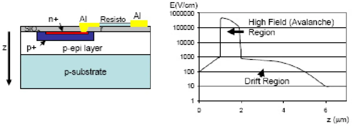
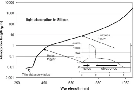
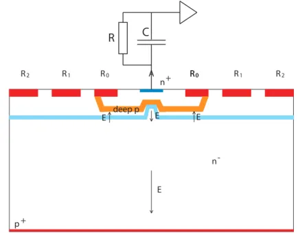
Silicon Photomultipliers (SiPM) are novel detectors for low level light detection based on arrays of avalanche photodiodes operating in Geiger mode. Though their quantum efficiency is already comparable or better than that of bialkali photomultiplier tubes it is still limited by the struc- tures on the light sensitive front surface. A new concept, presently developed at the Max-Planck semiconductor laboratory, allows boosting the efficiency to almost 100%. Using a fully depleted substrate the light enters through the unstructured backside. A drift diode structure collects the electrons on a small "point like" avalanche structure for multiplication. Engineering the thin en- trance window at the backside using anti-reflective layers a high efficiency can be achieved in a wide wavelength range (300-1000nm). Disadvantages are higher dark rate and increased cross- talk. Results from first test structures and device simulations will be presented. Applications in Particle Physics will be discussed.

International workshop on new photon-detectors PD07 June 27-29 2007

Kobe University, Kobe, Japan

Speaker.

(2)

PoS(PD07)005

1. Introduction

The Silicon Photomultiplier (SiPM) is a novel type of photon detector which allows for com- pact, robust, low cost devices with photon counting capability, high quantum efficiency, large gain and fast response ( < 100ps). In contrast to photo tubes SiPMs are insensitive to magnetic fields.

The development started about a decade ago, mainly in Russia [1–3]. When the first prototypes became available they triggered large interest for many applications, like calorimeters, air-shower Cerenkov telescopes, medical applications etc.

Figure 1: Principle SIPM cell (left). Electric fields in a SIPM (right)

A SiPM is a matrix of small geiger APDs (Avalanche Photodiode). Figure 1 shows a cross section of an individual pixel and the corresponding electrical field. Each pixel has an individual quenching resistor and the outputs of all pixels are connected together. The SiPM is operated at a voltage above the breakdown voltage. If a photon converts in the sensitive (=depleted) volume of such a pixel, the electron or hole drifts in the high field region and triggers the avalanche multiplica- tion, which discharges the diode capacitance C pixel . The multiplication process stops if the voltage drops below the breakdown voltage. Hence per pixel a charge of Q = C pixel ( U op U breakdown ) is re- leased. The quenching resistor R limits the current recharging the diode in order not to re-initialize the avalanche process. The pixel is active again after a recovery time τ rec = C pixel R. Hence a sin- gle cell is a binary device giving the same signal if one or more photons convert. In a matrix the signals of all cells are added. For low photon flux, if the probability for a single cell to be hit is very low, the output is simply proportional to the number of photons. However, for higher photon fluxes some cells might be hit by more than one photon leading to a nonlinear response and finally to saturation. In a crude approximation the dynamic range is given by the number of cells.

2. Limitations

At sufficiently high electric fields the efficiency for an electron or hole to trigger an avalanche

breakdown is almost 100%. Hence it should be possible to produce SiPMs with a Quantum Ef-

ficiency (QE) close to 100%. However, available devices have a much lower QE. The limiting

factors are:

(3)

PoS(PD07)005

Surface transmission: A fraction of the light is reflected at the surface of the entrance window or absorbed in the un-depleted surface layer, especially UV light.

Fill Factor: The major limitation of the present front illuminated devices is the fact that a substantial area of the pixel is inactive: space is needed for guard rings separating pixels electrically, bias resistors and Al-traces for electrical contacts. Therefore the resulting fill factor is always considerably lower than 100% and can be as low as 16% for small pixels.

It generally becomes better for larger pixel sizes, however, such devices may develop other problems (e.g. small dynamic range because of limited number of pixels).

Junction Type: At the same over voltage electrons have a considerable larger probability to trigger a Geiger breakdown than holes. For high efficiency at moderate overvoltage the device should be constructed in a way that the Geiger breakdown is preferentially initiated by electrons.

Another limitations of many SiPMs, especially for the detection of Cerenkov or blue/UV scintilla- tor light, is the modest sensitivity for blue and UV light. The wavelength dependence of the SiPM sensitivity is a consequence of the light absorption properties of silicon (Fig. 2). Three regions can be identified:

λ > 450nm: Most of the photons convert several microns deep in the silicon in or below the high field region. Due to the field configuration in p-type devices (to date standard) electrons drift back into the high field region. Electrons trigger avalanches efficiently, hence in this wavelength region the efficiency is high.

350nm < λ < 400nm: The photons are absorbed in the first microns of the device. Here holes drift into the high filed region and trigger the avalanche. Since holes have (at the same field) a lower probability to trigger an avalanche, the QE is reduced in this wavelength region.

λ < 350nm: The photons are absorbed in a thin surface layer. The electron/holes tend to recombine before they diffuse into the drift and finally high field region. In this region the QE drops sharply.

In order to increase the UV sensitivity the entrance window has to be made as thin as possible.

Using n-substrate instead of p-type the polarities of the electrical fields [4] and therefore the drift directions of electrons and holes are reversed. In such a design the avalanche is triggered by electrons for short wavelengths, however with a loss of sensitivity in the red.

Another disadvantage of SiPMs is the relative high dark rate due to thermally generated leak- age current. At room temperature dark rates can be several MHz for devices of a few mm 2 . Clearly the dark rate can be reduced by cooling.

The hot carriers (electrons and holes) in an avalanche emit light, about 2.9 photons per 10 5

electrons (E photon > 1.14eV [5]). These photons may travel to another pixel of the matrix and

initiate an avalanche breakdown there. As a result the average number of pixels fired per incident

photon is larger than one and the dark count distribution does not follow Poisson statistics. This

leads to additional noise and high dark rate even at larger threshold. The amount of cross talk

depends on many parameters, like pixel size, dead space between the active area, sensitive volume

(4)

PoS(PD07)005

Figure 2: Absorption length of light in Silicon as function of the wavelength. The insert shows the field shape in a SiPM made on p-type substrate.The drift directions of electrons and holes are indicated

and gain. One way to reduce cross talk is to optically insulate the pixels from each other by trenches etched around each pixel.

3. Back Illuminated SiPMs

Driven by the need for photon detectors with very high QE especially in the blue and UV for use in the MAGIC air Cerenkov telescope [6] MPI Munich started to develop SiPMs with backside illumination [7]. The basic structure of a single cell is shown in Fig. 3: Light enters through the unstructured backside and photons convert in the fully depleted n-type silicon bulk. Field shaping drift rings R 0 R n create an electric field in which the electrons drift into a small high field region where the avalanche multiplication occurs. This high field region is built up between the n + contact and the deep p implant. The latter is modulated in depth in order to confine the avalanche region to a small area. The advantages of this approach are:

The backside is unstructured and can be made very thin resulting in 100% fill factor and high conversion efficiency in a large wavelength range. In addition it is possible to coat the backside with anti-reflective layers enhancing the QE further.

The avalanche is always triggered by electrons giving high and uniform QE at moderate overvoltage and independent of the wavelength of the incident photon.

The avalanche region can be kept small resulting in small capacitance and low gain (which must still be kept high enough to have detectable signals). These can help to reduce cross talk and recovery time.

However, these advantages are counterbalanced by some disadvantages:

(5)

PoS(PD07)005

The whole silicon bulk must be depleted and the leakage current of this volume contributes to the dark rate. It is therefore important to use a process with low leakage current. Thinning of the device from nominal 450 μ m to about 50 μ m can reduce the bulk contribution further.

Still it may be necessary to cool the device in order to achieve an acceptable dark rate.

The large sensitive volume increases the cross talk. This must be compensated choosing a small gain and therefore the diode capacitance and the overvoltage should be as low as possible.

The drift of the electrons through the bulk towards the high field regions increases time jitter.

From simulation it is expected that the time resolution can still be kept below 2ns [8].

A more complicated production process (double sided processing) leads to higher costs.

First test structures have been produced and tested. These devices have an amplification struc- ture as shown in Fig. 3. In order to simplify production, they are not yet equipped with drift rings and backside contacts for full depletion. The aim of this production was to determine the preferred parameters of the avalanche structure.

-

p +

n+

n deep p

A R

0

R

1

R

2

R R R

000

R

1

R

2

R C

E

E E E

Figure 3: Principle of a backside illuminated avalanche diode.

A spectrum obtained with a 25 × 20 array of those structures is shown in Fig. 4. The photo- electron peaks are well separated, even for N > 15.

Leakage currents of these avalanche cells are low, the 500 pixel array have about 200 kHz dark

rate at room temperature. However, for the final back-illuminated devices the contribution of the

depleted bulk has to be added. Estimating from typical bulk currents achieved in our laboratory we

estimate the dark rate of a 0.25cm 2 device made on 50 μ m thin substrate to be about 10 MHz at

room temperature. By cooling to 0 o C the dark rate can be lowered to about 1 MHz.

(6)

PoS(PD07)005

Figure 4: Pulse height spectrum of a 500 pixel array illuminated with a 850 nm laser (pulse width < 1 ns).

The colours indicate different laser intensities.

As explained above cross talk is a major concern for back illuminated devices. The test arrays show a cross talk probability of 10 −4 . This may appear extremely low, however, it is because of the yet insensitive bulk. Using a Monte Carlo simulation we can extrapolate the measured rate to back side illuminated devices with a completely depleted bulk. The simulation results in a cross talk probability of 99% which would make the device useless. On the other hand the test structures have a very large gain, 4 × 10 6 , which is due to a relatively large avalanche region and especially a large coupling capacitance. The final arrays will have much lower gain, about 10 5 . Rescaling the photon emission probability the Monte Carlo predicts cross talk probabilities of 16% 30%. This may still be a bit larger than wanted by some applications, but it is already at an acceptable level.

Careful design modification, e.g. large pitch, can reduce this further.

Based on the results obtained with these test structures a new production with fully functional backside illuminated SiPMs including drift structures is presently processed in the MPI semicon- ductor laboratory. Amongst other structures it contains arrays of 30 hexagonal pixels with a pitch in the range of 100 μ m 200 μ m covering an area of 3 × 3mm 2 to 6mm 2 . The layout of a cell is shown in Fig. 5. The devices will become available end of 2007.

4. Applications

The development of the back illuminated SiPMs is focused on the application in the MAGIC

[6] camera. MAGIC is an air shower Cerenkov telescope situated on the island of La Palma. A

replacement of the present camera using photomultiplier tubes by SiPMs with large QE, especially

in the range 300-400 nm would reduce the energy threshold of the telescope dramatically. Timing

requirements and dark rates are not that critical. However, the implications of high cross talk needs

to be evaluated.

(7)

PoS(PD07)005

Figure 5: Layout of a backside illuminated SiPM presently in production. Shown is one cell with drift region (three drift rings) and the central avalanche region.

Backside illuminated SiPMs could be used in other applications, like scintillator readout for calorimeters or PET. This becomes interesting if high QE and UV response is needed and other properties like dark rate, timing and cross talk (and cost) are less important. There are some inter- esting aspects of the backside illuminated SiPM which make them attractive for further develop- ments:

Since all wirebond connections are on the surface opposite to unstructured entrance window such a SiPM can be coupled directly on a scintillator without air gap. This could enhance the light yield further.

A dedicated ASIC chip with an amplifier, threshold detection, signal processing and readout per pixel could be coupled to the SiPM with bump bonding or 3D integration techniques.

Such a device would allow single photon detection with single pixel position resolution.

References

[1] Z.Y. Sadygov, et al., IEEE Trans. Nucl. Sci, NS-43 (3), p. 1009 (2005) [2] Z.Y. Sadygov, et al. Proc SPIE 1621, p 158 (1991)

[3] B. Dolgoshein, Nucl. Instrum. Meth. A504, p. 48-52 (2003)

[4] K. Yamamoto, "Newly developed semiconductor detectors by Hamamatsu",these procedings [5] A. Lacaita et al., IEEE Trans. Electron Devices, ED-40, No 3, p. 577 (1993)

[6] J. A. Barrio et al., "Desing Report on MAGIC", MPI-PhE/98-5 (1998) [7] G. Lutz et al., IEEE Trans. Nucl. Sci. 52, p 1156 (2005)

[8] C. Merck, et al., Nucl. Instrum. Meth. A 567 (2006) 272.

Abbildung

Figure 1: Principle SIPM cell (left). Electric fields in a SIPM (right)
Figure 2: Absorption length of light in Silicon as function of the wavelength. The insert shows the field shape in a SiPM made on p-type substrate.The drift directions of electrons and holes are indicated
Figure 3: Principle of a backside illuminated avalanche diode.
Figure 4: Pulse height spectrum of a 500 pixel array illuminated with a 850 nm laser (pulse width &lt; 1 ns).
+2

Referenzen

ÄHNLICHE DOKUMENTE

In the more general case of imaging using a polychromatic (tube-)spectrum, a so-called spectral forward- model F i relates the basis material line-integrals to the registered

A n ungated inverse time-correlated single-photon count- ing system with a 120 M H z femtosecond dye laser excitation source was applied to the fluorescence lifetime, the molecular

MuTRiG: A Silicon Photomultiplier Readout ASIC with High Timing Precision and High.. Event

MAMI is a suitable facility for beam tests with high electron rates and high energy photons. The narrow high quality electron beam can be extracted at 855 MeV Tagged photon beam up

In a coherent field, the photonic quantum state has a well-defined phase; in an incoherent, thermal field, the phase information is distrib- uted randomly.. But on the

Left of the main Coulomb resonance, when the quantum dot is in its N electron state and the electrochemical potential of the N ↔ N + 1 resonance is above the bias win- dow, an

104, GR-10680 Athens, Greece f Department of Physics, University of Bergen, Allégaten 55, NO-5007 Bergen, Norway g Dipartimento di Fisica, Università di Bologna and INFN, Via

3.3.1 Determination of background track isolation e ffi ciency and related systematic uncertainties The fake photon track isolation efficiencies (ε B p and ε B f ) are estimated from