Topology and zero energy edge states in carbon nanotubes with superconducting pairing
W. Izumida, 1,2,* L. Milz, 2 M. Marganska, 2 and M. Grifoni 2
1
Department of Physics, Tohoku University, Sendai 980-8578, Japan
2
Institute of Theoretical Physics, University of Regensburg, 93040 Regensburg, Germany (Received 14 July 2017; published 11 September 2017)
We investigate the spectrum of finite-length carbon nanotubes in the presence of onsite and nearest-neighbor superconducting pairing terms. A one-dimensional ladder-type lattice model is developed to explore the low- energy spectrum and the nature of the electronic states. We find that zero energy edge states can emerge in zigzag class carbon nanotubes as a combined effect of curvature-induced Dirac point shift and strong superconducting coupling between nearest-neighbor sites. The chiral symmetry of the system is exploited to define a winding number topological invariant. The associated topological phase diagram shows regions with nontrivial winding number in the plane of chemical potential and superconducting nearest-neighbor pair potential (relative to the onsite pair potential). A one-dimensional continuum model reveals the topological origin of the zero energy edge states: a bulk-edge correspondence is proven, which shows that the condition for nontrivial winding number and that for the emergence of edge states are identical. For armchair class nanotubes, the presence of edge states in the superconducting gap depends on the nanotube’s boundary shape. For the minimal boundary condition, the emergence of the subgap states can also be deduced from the winding number.
DOI: 10.1103/PhysRevB.96.125414
I. INTRODUCTION
Single-wall carbon nanotubes (SWNTs) are one- dimensional (1D) crystals where the graphene honeycomb lattice, with its pseudospin valley degree of freedom, is rolled into a seamless cylinder. The finite curvature of the nanotube surface combined with the presence of valley and spin degrees of freedom is at the origin of a large variety of peculiar quantum transport properties, which have been intensively investigated in the last decades [1]. In recent studies, the emphasis has been put on the bound-state spectrum which naturally arises due to the finiteness of the SWNT length. It has been shown that the valley degeneracy of the bound states is not only lifted by the curvature-induced spin-orbit interaction [2–13], but also by a valley mixing from the edges [14,15].
Furthermore, open-ended SWNTs commonly host edge states whose energies lie in the bulk band gap [14,16,17]. Topological considerations can give a new perspective on the nature of these localized states. Recently, a one-to-one correspondence has been shown between the number of edge states and a winding number topological invariant [18], and that a topological phase transition can be induced by an external magnetic field [19].
Although the topological argument does not give a detailed information on the edge states (e.g., on their decay length), the use of topological invariants enables a general discussion on the emergence of the edge states, which is possible as long as the corresponding bulk system keeps the band gap.
When a superconductor is connected to a normal conductor, superconducting correlations leak into the normal conductor [20] and can give rise to a proximity-induced superconducting gap. In confined nanoconductors such as quantum dots and wires [21], resonant Andreev processes at the superconductor–
normal-metal interface cause the formation of bound states with excitation energies below the superconducting gap,
*
wizumida@tohoku.ac.jp
referred to as Andreev bound states. Such bound states have also been observed in SWNT-superconductor hybrid devices [22–27]. Reflecting superconducting correlations, the bound states correspond to entangled time-reversed electron-hole pairs and, hence, always come in pairs of opposite energy with respect to the center of the gap. Because the energy of the bound states depends on the microscopic details of the nanoconductor, in some systems it is possible to induce a crossing of the pair at zero energy upon variation of a gate voltage or of an external magnetic field [22,24,26]. Such states may like to stick at zero energy like a topological state, as pointed out in recent works on superconducting nanowires [28,29]. In this context, it is interesting to have the possibility to discriminate between nontopological bound states sticking at zero energy and truly topological zero energy bound states [30].
In this paper, we address theoretically the topological
origin of zero energy bound states localized at the edges of
a SWNT proximity coupled to a superconductor. On the one
hand, we perform numerical calculations of the spectrum of
SWNTs with length of a few micrometers which show that
zero energy edge states emerge in some regions of chemical
potential and proximity pairing strengths. These calculations
are based on a 1D lattice model which includes the effects of
curvature and superconductivity, and uses the helical-angular
symmetry of the system [31]. It extends the 1D lattice model
of Refs. [14,18,19] to the superconducting case. On the other
hand, the chiral symmetry of the bulk Hamiltonian allows us
to introduce a winding number as a topological invariant. We
show that the edge states emerge in the parameter region of
nontrivial, that is, nonzero, winding number. The condition for
the nontrivial winding number will be given in Eq. (32) [and
Eq. (34)]. The nontrivial winding number is the combined
result of the curvature-induced shift of the Dirac points from
the K or K points, and strong superconducting coupling
between nearest neighbors. Finally, a 1D continuum model
is introduced which allows us to obtain the condition for the
emergence of the edge states, which will be given in Eq. (43).
By comparing with the previously obtained condition for a nontrivial winding number, we find that these conditions are identical, hence proving the bulk-edge correspondence in our system. We notice that the formation of edge states depends not only on the chemical potential and the pairing potentials, but also on the chirality and the boundary shape of the nanotubes since they strongly affect the coupling of the two valleys.
Since the zero energy bound states appear in the induced superconducting gap region, these states can be regarded as Andreev bound states. In contrast to the conventional Andreev bound states, which extend in the whole of the nanoconductor, the zero energy bound states we observe are more specifically regarded as surface Andreev bound states, which in our case are also of topological origin [30,32].
Proximitized SWNTs in appropriately tuned magnetic or electric fields and with controlled gate voltage have been proposed as potential hosts of edge states of Majorana nature.
Their formation relies on the spin-orbit coupling (either native [33], or induced by an electric field [34], a spiral magnetic field [35], or a nuclear spin helix [36]), as well as on breaking the time-reversal symmetry. In our model, we do not include an external magnetic field, thus the time-reversal symmetry is preserved and the edge states always appear in pairs. In agreement with a recent work [37], we find no edge states if only an onsite pairing is present. Also, no edge states appear as long as the onsite pairing is larger than the nearest-neighbor one. The inclusion of large nearest-neighbor pairings results in the appearance of edge states which, interestingly, are just Dirac fermions.
This paper is organized as follows. In Sec. II, a formulation for superconducting SWNTs is given and the spectrum of the bulk system is presented. In Sec. III, the numerically calculated edge states in the superconducting gap are shown and discussed. In Sec. IV, the winding number is introduced as a 1D topological invariant and the topological phase diagram showing regions of nontrivial winding number is given. In Sec. V, a 1D continuum model is analyzed to show the physics of the emergence of edge states and the bulk-edge correspondence is proven. In Sec. VI, a case of strong valley coupling is studied on the example of the armchair class SWNTs. The conclusion is given in Sec. VII.
II. BOGOLIUBOV–DE GENNES HAMILTONIAN FOR FINITE-LENGTH SWNTS
A. Hamiltonian of a proximity-coupled SWNT Let us consider a SWNT proximity coupled to a supercon- ducting substrate [see Fig. 1(a)]. Proximity Hamiltonians have been investigated both in graphene [38,39] and in SWNTs [40].
Following Ref. [38], we model the π electrons in the SWNT in terms of a tight-binding Hamiltonian, which is given as the sum of a term H 0 describing the isolated system and of a term H sc accounting for proximity effects, H = H 0 + H sc . For later purpose, we first discuss some key features of the term H 0 before turning to H sc .
A SWNT is defined by rolling up a graphene sheet in the direction of the chiral vector C h = na 1 + ma 2 , where a 1 = ( √
3/2,1/2)a and a 2 = ( √
3/2, − 1/2)a are the unit vectors
A B
H C
h/ d a
1a
2δ
1 (1)δ
2 (1)δ
3 (1)δ
2 (2)δ
3 (2)δ
4 (2)δ
1 (2)δ
5 (2)δ
6 (2)z
A B ( n , m )=(6,3)
(b)
(c) (a)
Superconducting substrate SWNT z
a
zFIG. 1. (a) Schematic figure of a SWNT proximity coupled to a superconducting substrate. (b) Hexagonal lattice structure. Depicted are unit vectors a
1, a
2, alternative unit vectors C
h/d, H, and vectors to the nearest-neighbor and next-nearest-neighbor sites δ
(t)jfor an unrolled (n,m) = (6,3) SWNT, where d = gcd(n,m) = 3. A and B sublattices are denoted by gray and white circles, respectively. (c) An effective 1D lattice model, which is obtained by a partial Fourier transform in the circumferential direction, and is a projection of the 2D lattice structure onto the 1D nanotube axis z (see the dashed lines).
Solid lines denote nearest-neighbor bond connections in the original lattice structure.
of graphene, a = 0.246 nm is the lattice constant, and the set of the two integers (n,m) defines the geometrical structure, called chirality, of the SWNT [41] [see Fig. 1(b)]. The term H 0 , which includes curvature-induced effects [19], is explicitly given as follows:
H 0 = − μ c
rσ s
c † σrs c σrs +
⎛
⎝
rs
3 j = 1
γ s,j (1) c † Ars c Br +δ
(1) js + H.c.
⎞
⎠
+
rσ s
3 j =1
γ s,j (2) c † σrs c σ r +δ
(2)j
s + H.c., (1)
where c σ rs is the annihilation operator of one electron on sublattice σ ( = A,B) at site r and with spin s = ± 1. The spin quantization axis is chosen to be the nanotube axis. μ c sets the SWNT chemical potential and can be tuned, possibly, through external gate voltages. The vectors δ (1) j (j = 1,2,3) point to the three nearest-neighbor B sites from the A site, and the vectors δ (2) j (j = 1, . . . ,6) point to the six next-nearest-neighbor sites [see Fig. 1(b)]. A spin-independent shift of the Dirac points is included in the nearest-neighbor hopping, while spin-orbit effects influence both the nearest-neighbor and next-nearest- neighbor hoppings. Reflecting the time-reversal symmetry we have (γ − (t) s,j ) ∗ = γ s,j (t) . The explicit forms of the vectors δ (t) j and the hopping integrals γ s,j (t) (t = 1,2) are provided in Appendix A 1.
Regarding the effective pairing Hamiltonian H sc , we notice
that the diameter d t of a SWNT is much smaller than a typical
superconducting penetration length λ > 10 nm [20]. Then,
we can assume singlet superconducting pairing terms 0 , 1
being constant on the whole lattice, yielding [38]
H sc = 0
rσ
c † σr ↑ c † σr ↓ + H.c.
+ 1
r
3 j = 1
(c † Ar ↑ c †
Br +δ
(1)j↓ − c † Ar ↓ c †
Br +δ
(1)j↑ +H.c.).
(2) Here, we have alternatively used s = ↑ , ↓ for the spin index.
The term proportional to 0 represents the onsite pairing, and the term proportional to 1 the pairing between the nearest-neighbor sites. The gauge freedom allows us to choose the coupling terms 0 , 1 as real numbers. To determine the precise values of 0 and 1 for a given chirality of SWNT contacted to a superconducting substrate, a microscopic anal- ysis of the interactions between the superconducting substrate and the SWNT would be needed [40], in principle including also pairing correlations between next-nearest and further neighbors. However, as will be shown below, the presence of nearest-neighbor pairing is the minimum requirement for the presence of nontrivial topological phases. Therefore, in this paper we treat both 0 and 1 as parameters in order to study their interplay.
B. The 1D lattice Hamiltonian in the helical-angular construction
Due to the C d rotational symmetry of a SWNT with respect to the tube axis, the orbital angular momentum L z = hμ ¯ is a well-defined quantity, which is characterized by the integer
μ = 0,1, . . . ,d − 1. (3) Here, d = gcd(n,m) is the greatest common divisor of n and m. Note that the angular momenta μ and μ are equivalent if mod(μ − μ ,d ) = 0, thus, e.g., μ = −1 is equivalent to μ = d − 1. Furthermore, also the spin component along the SWNT axis is a conserved quantity, which allows us to decompose the Hamiltonian into μ ≡ (μ,s) subspaces. The decomposition is performed by a partial Fourier transform in the circumference direction. To achieve this, it is convenient to use the helical-angular construction [18,19,31] in which the atomic position r is expressed by the alternative unit vectors C h /d and H, where H = p s a 1 + q s a 2 with the integers p s
and q s satisfying mp s − nq s = d . It holds r = ν(C h /d ) + H + δ σ,B δ (1) 1 with the two integers ν = 0,1, . . . ,d − 1 and . The integer indicates the lattice position in the axis direction in units of a z = √
3ad/2 √
n 2 + m 2 + nm, which is the shortest distance between σ atoms in the axis direction [see Fig. 1(b)]. In this framework, the two-dimensional (2D) wave vector is expressed as k = μ Q 1 /d + k Q 2 /(2π/a z ), where k is the wave number along the nanotube axis defined in the 1D Brillouin zone (BZ) − π/a z k < π/a z , and Q 1 and Q 2 are the two reciprocal lattice vectors conjugated to C h /d and H, respectively. That is, the relations Q 1 · C h /d = Q 2 · H = 2π and Q 1 · H = Q 2 · C h /d = 0 hold. Then, the partial Fourier
TABLE I. Hopping distance δ
(tj)and phase factor δν
j(t)in the 1D lattice model [18,19]. The integers p
sand q
ssatisfy mp
s− nq
s= d, where d = gcd(n,m).
j = 1 j = 2 j = 3 j = 4 j = 5 j = 6 δ
(1)j−
n−3dm 2n3d+m−
2m3d+nδν
j(1) ps−3qs−
2ps3+qs 2qs+3psδ
(2)j md n+dm dn−
md−
n+dm−
ndδν
j(2)− q
s− (p
s+ q
s) − p
sq
sp
s+ q
sp
stransform is expressed as c σ rs = 1
√ d
d −1
μ = 0
exp i 2π d νμ
c σ μ . (4) The Hamiltonian of the normal term is rewritten as H 0 =
μ H 0, μ , where [14,18,19]
H 0, μ = − μ c
σ
c σ † μ c σ μ
+
3 j =1
e i
2πdδν
j(1)μ γ s,j (1) c † A μ c B
(1)j
μ + H.c.
+
σ
3 j =1
e i
2πdδν
j(2)μ γ s,j (2) c † σ μ c σ
(2)j
μ + H.c., (5) where
(t) j = + δ (t) j , t = 1,2. (6) The hopping distance δ (t) j and the phase factor δν j (t) are determined from δ (t) j = δν j (t) C h /d + δ (t) j H. Their explicit expressions are given in Table I. As schematically shown in Fig. 1(c), the Hamiltonian in each μ subspace represents a ladder-type 1D lattice model [18,19,31].
Under the partial Fourier transform of Eq. (4), the super- conducting term of the Hamiltonian takes the form
H sc =
μ
0 2
σ
sc † σ μ c † σ −μ + H.c.
+ 1
3 j = 1
e i
2πdδν
(1)jμ sc † A μ c †
B
(1)j−μ + H.c.
. (7) The pair μ and −μ in the superconducting term reflects the conservation of angular momentum and spin.
C. Bogoliubov–de Gennes formalism for the 1D lattice Hamiltonian
Since the total Hamiltonian H 0 + H sc has a bilinear form
in the fermionic operators c σ μ , the excitation spectrum is
conveniently calculated within the Bogoliubov–de Gennes
(BdG) formalism [20]. The BdG Hamiltonian H is given
by doubling the fermionic operators upon introduction of the
Nambu spinor
c † σ μ = (c † σ μ ,c σ −μ ), c σ μ = c σ μ
c σ † −μ
. (8) For instance, the superconducting term proportional to 0 in Eq. (7) is rewritten as
0
s
sc † σ μ c σ † −μ + H.c. = 0
s
sc † σ μ π ˆ x c σ μ . (9) Here, we have introduced the Pauli matrices ( ˆ π x , π ˆ y , π ˆ z ) acting in the particle-hole subspace. Detailed transformation to the BdG form of the superconducting term proportional to 1 in Eq. (7) is given in Appendix A 2. Collecting all terms, the BdG Hamiltonian for the SWNTs is expressed as H = 1 2
μ H μ , where
H μ =
σ
c † σ μ ( − μ c π ˆ z + s 0 π ˆ x )c σ μ
+
⎡
⎣
3 j =1
e i
2πdδν
(1)jμ c † A μ
γ s,j (1) π ˆ z + s 1 π ˆ x
c B
(1)j
μ
+
σ
3 j = 1
e i
2πdδν
j(2)μ γ s,j (2) c † σ μ π ˆ z c σ
(2)j
μ + H.c.
⎤
⎦. (10)
In each μ subspace H μ represents a 1D ladder Hamiltonian, which extends to the BdG form a previously developed 1D lattice model for the normal state [14,18,19].
The doubling also gives a particle-hole symmetry to the BdG excitation spectrum. The BdG spectrum in a finite- length SWNT with = 1,2, . . . ,N L lattice sites is numerically calculated by diagonalizing the Hamiltonian in Eq. (10), and will be analyzed in Sec. III. Before doing this, we discuss the BdG spectrum of the bulk system.
D. Energy bands and BdG spectrum of the bulk system Exploiting translational invariance, the BdG Hamiltonian of the bulk system is written in the Bloch basis as H μ =
k c † k μ H μ (k)c k μ , where
H μ (k) = ε c, μ (k) f e, μ (k) f e, ∗ μ (k) ε c, μ (k)
ˆ π z
+ s 0 f eh,μ (k) f eh,μ ∗ (k) 0
ˆ
π x (11) and
f e, μ (k) = 3 j = 1
γ s,j (1) e ik ·δ
(1)j, f eh,μ (k) = 1 3 j = 1
e ik ·δ
(1)j,
ε c, μ (k) = − μ c + ε so, μ (k), ε so, μ (k) = 6 j = 1
γ s,j (2) e i k ·δ
(2)j. (12) The Nambu spinor in k space is c † k μ = (c † Ak μ ,c † Bk μ , c A − k −μ ,c B − k −μ ) with c σ k μ = √ 1 N
L
exp (− ika z )c σ μ , and k = (μ,k). The BdG spectrum of the bulk system is obtained by diagonalizing the Hamiltonian matrix of Eq. (11).
(n,m)=(6,3)
ε
μ(eV)
ka
z–8
–6 –4 –2 0 2 4 6 8
–3 –2 –1 0 1 2 3
μ =2 μ =0 μ =1
(n,m)=(8,2)
μ =1 μ =0
ka
z–3 –2 –1 0 1 2 3
(a) (b)
μ =0
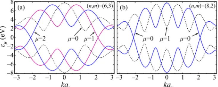
FIG. 2. Conduction and valence bands of (a) (n,m) = (6,3) metal-1 SWNT, classified into the zigzag class, and (b) (n,m) = (8,2) metal-2 SWNT, classified into the armchair class. For both cases (a) and (b), p
s= 1 and q
s= 0. The angular momentum for each band is indicated, the blue curves show bands with μ = μ
K, and the purple curves in (a) show bands with μ = μ
K. Curvature-induced energy gaps at zero energy and spin-orbit splitting are not seen on this energy scale.
1. Energy bands for the normal case
Before showing the BdG spectrum of the bulk system, we shall review the energy bands of the normal case. Until discussing the BdG spectrum, we set the chemical potential to be zero, μ c = 0. The conduction and the valence bands of the SWNTs are given by diagonalizing the matrix in the first term of Eq. (11) and have the standard form [1]
ε μ (k) = ε so, μ (k) ± | f e, μ (k)| , (13) where the signs + and − correspond to the conduction and the valence bands, respectively.
It is well known that the SWNTs are metallic when mod(2n + m,3) = 0 and semiconducting if mod(2n + m,3) = 1,2 [41]. Recent studies [14,15,18,42] have revealed that the SWNTs can be alternatively classified into two classes accord- ing to the angular momentum of the two valleys, denoted in the following K and K : (i) zigzag class, which includes metal-1 (metallic SWNTs with d R = d ) and semiconducting SWNTs with d 4, in which the two valleys have different angular momenta, where d R = gcd(2n + m,2m + n); (ii) armchair class, which includes metal-2 (metallic SWNTs with d R = 3d) and semiconducting SWNTs with d 2, in which the two valleys have the same angular momentum. Here, the angular momentum μ τ of valley τ (= K,K ) is defined as follows.
For the metallic SWNTs, μ τ is the angular momentum at the τ point, which is given by μ τ = mod[τ (2n + m)/3,d]
[18], where we have alternatively used τ = 1 (−1) for the valley K (K ). At the same time, the 1D wave number for the τ point is given by k τ = (2π/3a z )mod[τ (2p + q ),3] [18].
For the semiconducting SWNTs, the corresponding angular momenta and the 1D wave numbers are given by the ones which are closest to the τ point. Their explicit expressions are also given in Ref. [18].
Specifically, μ K = μ K
= 0 holds for the metal-2 SWNTs
[14]. Figure 2 clearly shows the above features: in Fig. 2(a)
we depict the energy bands of an (n,m) = (6,3) SWNT which
belongs to the zigzag class. The angular momentum μ K = 2
of valley K is different from that of the K valley which is
μ K
= 1. On the other hand, Fig. 2(b) shows the energy band
( n , m )=(6,3)
–0.5 0 0.5
ε BdG (eV)
–2.3 –2.2 –2.1 –2
ka z ε μ (eV)
0 0.5 1.0
(a)
(b) k –
( K , s )
k + ( K , s )
–1.0 –0.5 0.5 1.0
–2.2083 –2.2078 0
(meV)
s=1 s=–1
–1.0 –0.5 0.5 1.0
–2.05345 –2.05295 0
(meV)
s=–1 s=1
FIG. 3. (a) Energy band, and (b) BdG excitation spectrum near the K point for an (n,m) = (6,3) SWNT. The chemical potential is set to be μ
c= 500 meV. The two arrows with k
(K,s)±in (a) indicate the two Fermi points. In (b) the superconducting coupling parameters are chosen to be
0= 0.5 meV and
1= 2 meV. Each inset in (b) shows the enlarged BdG spectrum near the two Fermi points. The blue and red curves show the BdG spectra for the spin-up and -down components, respectively.
of an (n,m) = (8,2) SWNT, representative of the armchair class, where μ K = μ K
= 0.
Since we are focusing on the states near the K and K valleys, it is sufficient to consider a limited number of μ subspaces, which are specified by the angular momenta of the valleys. In the following, we focus on the zigzag class SWNTs where two valleys are well decoupled. The armchair class will be discussed in Sec. VI.
2. BdG spectrum of zigzag class SWNTs
Since our interest is on the impact of superconductivity on the conducting electrons, the chemical potential will be set in the energy region corresponding to electron transport.
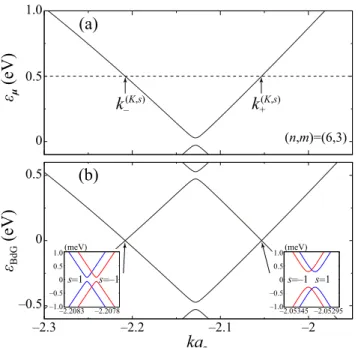
Figure 3(a) shows the energy bands near the K point for an (n,m) = (6,3) SWNT. The dashed line indicates the chemical potential. Figure 3(b) shows the corresponding BdG spectrum.
As shown in the two insets, the BdG spectrum exhibits small superconducting gaps of the order of the superconducting couplings near the two Fermi points k = k − (τ ) and k = k (τ) + (>
k − (τ) ), at which
μ c = ε μ
τk r (τ)
(r = ±1) (14) is satisfied in the τ valley, where τ ≡ (τ,s), μ τ ≡ (μ τ ,s), and ε μ
τ(k (τ) r ) is the single-particle energy of band μ τ at k (τ) r given by Eq. (13).
For a moderate chemical potential | μ c | 1 eV, the k · p scheme can be used. The hopping functions f e, μ and f eh, μ are
expanded around the τ point as [7]
f e, μ (k) cγ [(k z − τ k z ) + i(k c − k c, τ )], f eh,μ (k) c 1 (k z + ik c ), ε c, μ (k) − μ c, τ , (15) where c is a complex coefficient encoding the chiral angle and valley with | c | = √
3a/2, and
k c, τ = k c + τ sk so , μ c, τ = μ c − τ sε so . (16) Here, k z , k c are the curvature-induced shifts of the Dirac point from the K point in the circumferential and the axial directions, respectively. k so and ε so are the spin- dependent Dirac point shift in the circumferential direction and the Zeeman-type energy shift, respectively, induced by the spin-orbit interaction. Their explicit expressions are given in Eqs. (A4) and (A5) in Appendix A 1. Finally, k z and k c are the wave numbers in the circumferential and axial directions measured from the τ point, and k c = 0, −2/3d t , and 2/3d t for metallic, type-1 [mod(2n + m,3) = 1], and type-2 [mod(2n + m,3) = 2] semiconducting SWNTs, respectively.
Using Eq. (15), the two Fermi points measured from the τ point are given by
k (τ) r = τ k z + r μ c, τ
| c | γ 2
− (k c − k c, τ ) 2 . (17) And, as shown in Appendix B, the superconducting gap near k ( r τ ) is expressed as
ε (τ) g,r = 2 0 + 2 1
μ c, τ γ
1 + ε c, τ E c, τ
− rτ sgn(μ c, τ )ε z, τ
1 − E 2 c, τ
, (18) where
E c, τ = | c | γ (k c − k c, τ )
μ c, τ , ε c, τ = | c | γ k c, τ
μ c, τ ,
ε z, τ = | c | γ k z
μ c, τ . (19)
Since the absolute value of the numerator of E c, τ expresses the half of the bulk band gap, the relation | E c, τ | < 1 holds when the chemical potential is in the energy band regions. It should be noted that the superconducting gaps at the two Fermi points k ( r τ ) (r = ± ) are different as shown in the inset of Fig. 3(b) as well as expressed in Eq. (18). This is because the contribution of 1 to the superconducting gap is k dependent, as shown in Eq. (15), and the contribution at the two Fermi points is different, reflecting the shift k z of the Dirac point. The two different superconducting gaps at the two Fermi points play an important role in the emergence of edge states, as will be discussed later.
Next, we focus on the low-energy BdG excitations, of the order of the superconducting gaps, in finite-length SWNTs.
III. BdG SPECTRUM IN FINITE-LENGTH SWNTS
We focus on an (n,m) = (6,3) SWNT with N L = 2 × 10 5 ,
which corresponds to a SWNT length of 16.1 μm, as an
example for the zigzag class SWNTs. The BdG Hamiltonian
( n , m )=(6,3), L
NT=16.1μm, μ=( μ
K,1)
Δ
1(meV) ε
BdG(meV)
0.3 0.4 0.5 0.6 0.7 0.8 0.9 μ
c(eV)
1.0 0.6
0.4
0 –0.2 –0.4 –0.6 0.2
2
0 1 3 4
Δ
0=0.5meV Δ
1=2meV μ
c=0.65eV
Δ
0=0.5meV
(a) (b)
Reφ Reφ
ε
g,–1ε
g,+1ε
g,–1ε
g,+11 N
FIG. 4. BdG spectrum of a (6,3) nanotube with a length of 16.1 μm in the μ = (μ
K= 2,1) subspace. (a) Spectrum as a function of the superconducting pairing
1, and (b) as a function of the chemical potential μ
c. Blue circles show the calculated spectrum and the dashed lines show the superconducting gaps ε
g,r(K,s=1)of the bulk system given in Eq. (18). The inset in (b) shows the real part components φ
χA(blue) and φ
ξA(red) in arbitrary units as a function of lattice site for the calculated eigenfunction at ε
BdG= 0 with
0= 0.5 meV,
1= 2 meV, and μ
c= 650 meV [indicated by the red arrow in (b)]. The definition of φ
pσ(p = χ ,ξ ) is given in Eq. (22).
is diagonalized as
H μ =
l
vε BdG (μ l
v) b † μ l
v
b μ l
v, (20)
where l v enumerates the quasiparticle energy levels, and b μ † l
v
=
σ
φ pσ (μ l
v) ()c † σ μ + φ hσ (μ l
v) ()c σ −μ
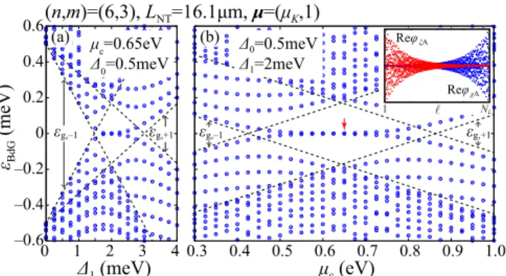
. (21) Figure 4 shows the calculated spectrum in the energy region of the order of the superconducting gaps in the subspace μ = (μ K = 2,1). The boundary shape is depicted in Fig. 1(c), which belongs to the class of so-called minimal boundaries.
The eigenvalue solver FEAST [43] of the Intel Math Kernel Library was used for the numerical calculation. The dashed lines show the evolution of the superconducting gaps ε ( g,r τ ) given in Eq. (18) with 1 [Fig. 4(a)] and μ c [Fig. 4(b)]. The functions φ χA , φ ξ A shown in the inset of Fig. 4(b) are connected to φ pA , φ hA by a unitary transformation
φ χ σ φ ξ σ
= U π − 1 φ pσ φ hσ
, (22)
where
U π = 1 2
1 + i 1 + i
− 1 + i 1 − i
. (23)
We will discuss this transformation in the next section. In the region 1.5 1 3 meV in Fig. 4(a) and 400 μ c 900 meV in Fig. 4(b), states near zero energy exist inside the gap region. As shown in the inset in Fig. 4(b), these states are localized at the edges and their nature will be discussed in the coming sections. Calculations for the other three subspaces, (μ K , − 1) and (μ K
, ± 1), where μ K
= 1, exhibit an almost identical behavior (not shown) as the one seen in Fig. 4. Emergence of the zero energy states in these regions is also seen (not shown) for other boundary shapes,
e.g., when removing or adding a A sublattice at the end of the boundary shown in Fig. 1(c).
The numerical result in Fig. 4 clearly shows that there exist edge states at zero energy in some parameter regions.
To explore the condition for the emergence of the edge states, we will analyze the bulk system from a topological viewpoint.
IV. WINDING NUMBER
Let us again consider the bulk Hamiltonian given in Eq. (11). Since the Hamiltonian has the chiral symmetry { , H μ } = 0, where = π ˆ y , one can introduce the winding number
w μ = − 1 4π i
π/a
z− π/a
zdk Tr
H − μ 1 (k)∂ k H μ (k)
(24) as a 1D topological invariant [44,45]. The identity with another definition of the winding number, which uses a flat band Hamiltonian [46], is proven in Appendix C 1. Let us consider the unitary transformation U π defined in Eq. (23), which rotates the Pauli matrices for the particle-hole basis as U π † π ˆ x U π = π ˆ y , U π † π ˆ y U π = π ˆ z , U π † π ˆ z U π = π ˆ x . Correspond- ingly, the Hamiltonian in Eq. (11) takes in the following an off-diagonal form
H ˜ μ (k) = U π † H μ (k)U π =
0 h μ (k) h † μ (k) 0
, (25) where
h μ (k) = ε c, μ (k) − is 0 f e, μ (k) − isf eh,μ (k) f e, ∗ μ (k) − isf eh,μ ∗ (k) ε c, μ (k) − is 0
.
(26) At the same time, the fermionic operators are transformed as
c χ σ k μ c ξ σ k μ
≡ U π − 1 c σ k μ
c † σ − k −μ
. (27)
Because the chiral operator is transformed as ˜ = U π † U π = ˆ
π z , the winding number is written as w μ = 1
2π π/a
z− π/a
zdk∂ k arg det h μ (k), (28) with the determinant of h μ (k) being
det h μ = ε c, 2 μ − 2 0 − | f e, μ | 2 + | f eh,μ | 2
+ 2is ε c, μ 0 + f e, μ f eh,μ ∗ + f e, ∗ μ f eh,μ 2
(29) (see Appendix C 2 for the derivation).
For the case of | 0 | , | 1 | | μ c | , | γ |, on which we are focusing, the real part of det h μ is expressed as
Re(det h μ ) ε c, 2 μ − | f e, μ | 2
= [− μ c + ε so, μ ] 2 − | f e, μ | 2 . (30) Except near the Fermi points, we have
| Re(det h μ ) | | Im(det h μ ) | (31)
–2.3 –2.2 –2.1 –2 ( n , m )=(6,3) μ = μ
Kka z ar g det h μ
π 2π
0
s=1
s=–1 –π
3π
FIG. 5. Phase of det h
μ, arg det h
μ, appearing in the integrand of the winding number in Eq. (28), for an (n,m) = (6,3) nanotube near the K point for which the angular momentum is μ
K= 2. The parameters are the same as those in Fig. 3(b). The continuous change of the function in the interval −π arg det h
μ3π is clearly seen.
The blue and red curves show the spin components s = 1 and − 1, respectively. Note that both of them are almost equal π in the regions of ka
z− 2.21. For this case, the integrand gives contribution + 1 ( − 1) to the winding number for s = 1 (s = − 1).
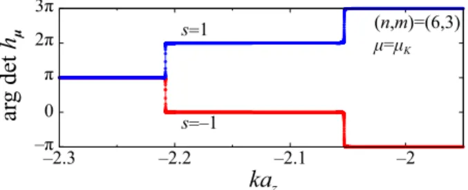
since the imaginary part of det h μ is proportional to the superconducting pairing potentials 0 and 1 . Therefore, Eq. (29) is approximated as a positive or negative real number, and then the phase of det h μ is almost constant and equal to 0 or π . This feature is clearly observed in Fig. 5, which shows the phase of the determinant of h (μ
K,s) near the K point.
Let us focus on the regions near the Fermi points at the τ valley, which are the only ones where the phase of det h μ
τchanges and a finite contribution to the integral in Eq. (28) is expected, as can be seen in Fig. 5. As seen in the k · p scheme, in which the functions f e, μ and f eh, μ have the form in Eq. (15), Re(det h μ
τ) behaves quadratically in k near the τ point. That is, Re(det h μ
τ) is negative for k z < k − (τ ) and k z > k + (τ ) , and is positive for k (τ) − < k z < k + (τ ) . Note that the two roots of Re(det h μ
τ) are regarded as the two Fermi points in our approximation of small superconducting couplings.
Let us define h (τ) r ≡ h μ
τ(k r (τ) ), the function h μ
τat the Fermi point for the τ valley. When Im(det h ( + τ ) ) has the opposite sign of Im(det h ( − τ ) ),
Im(det h ( + τ ) )Im(det h ( − τ ) ) < 0, (32) then det h μ near the Dirac point contributes to a nontrivial winding number (see the schematics in Fig. 6). Note that the maximum contribution to the winding number per Dirac point is | w μ | = 1 because of the above discussion. The sign of the winding number is given by the sign of Im(det h (τ + ) ), that is, the winding number is
w μ = sgn[Im(det h (τ) + )]| w μ | . (33) Figure 7 shows the topological phase diagram for an (n,m) = (6,3) nanotube calculated from Eq. (32) for (τ,s) = (1,1).
Within the k · p approximation, after some algebra given in Appendix C 2, the condition (32) is summarized
k
+k
–0 Re(det h
μ) Im(det h
μ)
det h
μ( k )
arg det h(k)
FIG. 6. Schematics of the trajectories of the complex function det h
μin the complex plane when k changes from k k
−to k k
+. The solid curve shows an example for a nontrivial winding number w
μ= 1, and the dashed curve shows a case for a trivial winding number w
μ= 0.
as
γ
μ c, τ + 1
0 1 + ε c, τ E c, τ 2
− ε 2 z, τ 1 0
2
1 − E 2 c, τ
< 0. (34) Using the relation
Im
det h ( r τ )
= sμ c, τ ε g,r ( τ ) , (35) which is given in Appendix B [after Eq. (B18)], the sign of the winding number can also be evaluated. As seen in Eq. (34), the condition holds only when ε z, τ = 0, that is, k z = 0, the case of a finite shift of the Dirac point in the
30 20 10
–30 –20 –10
0 0.5 1.0
–0.5 –1.0
μ
c(eV) Δ
1/ Δ
00
w
μ=1 w
μ=–1
0.408 0.409 3.995
4.000 4.005
w +w =1
FIG. 7. Topological phase diagram for an (n,m) = (6,3) nan- otube estimated from Eq. (32) for (τ,s) = (1,1) in the μ
cand
1/
0plane, where
0= 0.5 meV. The light blue areas show the region
of nontrivial winding number, | w
μ| = 1. The dashed curves show
Eq. (36), the analytical expression for the border of the topological
phases. The region between the dashed vertical lines is the band-gap
region of the normal state. The red lines indicate the parameter
region of Fig. 4. The inset shows the phase diagram for the value
w
(μ,1)+ w
(μ,−1)near the region marked by the red point, which has a
nontrivial value only near the border of the main figure.
axial direction, and 1 = 0. Note that E c, 2 τ < 1 holds outside the energy gap of the nanotubes. As shown in Eq. (A4), we have a finite k z except for the pure zigzag SWNTs, for which the chiral angle is θ = 0. We also notice that the condition (34) depends on the ratio of 0 and 1 but not on their absolute values.
At the border, one of the two superconducting gaps ε g,r ( τ ) (r = ±) becomes zero. Then, from the condition ε (τ) g,r = 0 and Eq. (18), the border is determined by
1 0
= − γ μ c, τ
(1 + ε c, τ E c, τ ) + rτ sgn(μ c, τ )
ε 2 z, τ
1 − E 2 c, τ (1 + ε c, τ E c, τ ) 2 − ε 2 z, τ
1 − E 2 c, τ . (36) Note that the border is also given by the roots of the left-hand side of Eq. (34). By comparing with the numerical calculation in Fig. 4, we confirm that the zero energy edge states appear in the region where the winding number has a nonzero value.
The region becomes narrower and the borders asymptotically behave as 1 / 0 − γ /μ c for a large μ c . This implies that to have nontrivial winding number, the ratio δ = 1 / 0 becomes smaller and comparable to 1 for | μ c | ∼ | γ |, as shown in Fig. 7.
However, such a chemical potential might be unrealistically large.
Let us comment on the effect of the spin-orbit interaction.
As shown in Eq. (16), the spin-orbit interaction gives the spin dependence in the phase diagram. Since we are focusing on the conducting region for the normal state, we have | μ c |
| ε so | . Furthermore, we also have the relation | k c | | k so | except for the armchair SWNTs. For the armchair SWNTs, the spin-orbit interaction opens a small gap at μ c = 0, as already pointed out in previous studies [2–4,7]. Therefore, we have an almost identical phase diagram for the (τ,s) and (τ, − s) subspaces except for the sign difference reflecting the opposite winding direction between s and − s, as seen in the relation (35). A small difference between the opposite spins, shown as the finite value of w (μ
K,1) + w (μ
K, − 1) in the inset of Fig. 7, appears at the border region scaled by the spin-orbit interaction. Note that the phase diagrams for (τ,s) and (− τ, − s) are the same including the sign. Therefore, the total winding number
τ,s w μ
τ= 2(w (μ
K,1) + w (μ
K, −1) ) shows the same diagram as w (μ
K,1) + w (μ
K, − 1) . As a result, the total winding number is nonzero only in very narrow regions of the parameter space. Nevertheless, several edge states are present in the nanotube even when the total winding number is zero, which proves that the total topological invariant may miss a rich part of the physics of the system.
As a further example, it should be noted that in the armchair class, with μ k = 0 = μ K , the winding number w μ becomes zero even when the condition (34) is satisfied for both valleys.
This is because the winding directions for the τ and − τ valley are opposite, which can be seen from the relation (35).
However, this does not mean that there is no edge state for the armchair class, as will be discussed in Sec. VI.
Let us comment on the symmetry class to which our 1D model belongs according to the topological classification in
Ref. [46]. Since we have only the chiral symmetry in each μ subspace, the 1D model in that space belongs to the AIII class. The total Hamiltonian has time-reversal symmetry, and belongs to class DIII. Further discussion on the different topological invariants in our system can be found in Appendix C 3.
It should be noted that the nontrivial topological phase obtained in our work does not contradict a previous study [37], which predicts only a trivial topological phase if the induced superconducting correlation is s wave. This correlation appears in our Hamiltonian as the onsite pairing. As already mentioned, the 1 term, which is the coupling constant for the k-linear term in Eq. (15), and thus acts as the p-wave superconducting coupling [38], is needed to have the nontrivial topological phases.
V. BULK-EDGE CORRESPONDENCE
In this section we shall reveal the deep physical meaning of the condition constituting Eq. (32). As mentioned in the Introduction, it has been shown [18] for the SWNTs in the normal state that the winding number per μ space w μ is equal to the number of edge states in this space. The latter are given by the difference between the number of evanescent modes, being the solutions of the mode equation at zero energy, and the number of boundary conditions for given sublattice.
This gives a one-to-one correspondence between the winding number as a topological invariant and the physical edge state.
This kind of relation is called a bulk-edge correspondence.
Let us discuss the bulk-edge correspondence for the present system by including the finite length of the SWNT in our description.
Since the relevant contribution to the winding number comes from the neighborhood of the τ point, we shall consider an effective 1D continuum model obtained by expanding around the τ point. The envelope function
τ = χ τ
ξ τ
, p τ = pAτ pBτ
(37) obeys the equation
H ˆ˜ μ
τ( ˆ k z ) τ = ε τ , (38) where p = χ ,ξ, and ˆ˜ H μ
τ( ˆ k z ) has the same functional form of Eq. (25) with Eq. (15). However, the wave number k z is now regarded as the operator
k ˆ z = − i ∂
∂z (39)
in the continuum model. At zero energy, ε = 0, the equation can be divided into two sets of equations with 2 × 2 matrix forms:
h ˆ p μ
τ( ˆ k z ) p τ = 0, (40) where ˆ h χ μ
τ( ˆ k z ) and ˆ h ξ μ
τ( ˆ k z ) are given by changing k z → k ˆ z in h † μ
τ(k z ) and h μ
τ(k z ), respectively. Let us consider the modes with the following form:
p τ = e iqz 1 η p
. (41)
In each p block, the modes obey the following equation:
− μ c, τ + ips 0 c[γ (q − τ k z ) + ips 1 q] + c[iγ (k c − k c, τ ) − ps 1 k c ] c ∗ [γ (q − τ k z ) + ips 1 q ] − c ∗ [iγ (k c − k c, τ ) − ps 1 k c ] − μ c, τ + ips 0
× 1 η p
= 0, (42)
where we have alternatively used the index p = 1 and −1 for p = χ and ξ , respectively. To have nontrivial solutions, the determinant of the matrix in Eq. (42) should be zero. Since this gives a second-order equation in q, there exist two modes corresponding to the solutions q r (τ) . A relation between q r (τ) and the Fermi point k r ( τ ) will be shown in Eq. (44).
Within the continuum model, the microscopic boundary condition is implicitly taken into account in order to form eigenstates. They are constructed as linear combinations of two independent modes, a leftgoing and a rightgoing one, subject to boundary conditions at each end. Note that in the superconducting gap region the two modes are two decaying modes, that is, | κ r (τ) | < 1 or | κ r (τ) | > 1, where κ r ≡ Im(q r (τ ) ).
If the two modes have the same decaying direction, that is, κ + ( τ ) κ − ( τ ) > 0, (43) then an edge state given by the linear combination of the two modes appears at an end. In the following, we explicitly show that this condition is identical to the condition (32) for nontrivial winding number.
As shown in Appendix D, we arrive after some algebra to the two solutions
Re q r (τ)
k r (τ) , κ r (τ ) rps sgn(μ c, τ )
| c | γ
1 − E c, 2 τ ε ( g,r τ )
2 . (44) Since we have the relation (35), we get
κ r (τ ) = rp Im
det h ( r τ ) 4| μ c, τ || c | γ
1 − E c, 2 τ
. (45)
Combining Eqs. (43) and (45), it is immediately clear that the condition for emergence of an edge state is identical to the condition for a nontrivial winding number expressed by Eq. (32).
It is worth noting that, from Eq. (44), the decay length of the edge state is proportional to the Fermi velocity,
−| c | γ √
1 − E c, 2 τ /¯ h, of the normal states at the given chemical potential and is inversely proportional to the superconducting gap. This implies the shortest decay length to be near the bottom of the conduction or top of the valence bands for the semiconducting SWNTs.
VI. ARMCHAIR CLASS
So far, we have been restricting ourselves to the case of decoupled valleys. Let us discuss the effect of valley coupling by considering the armchair class SWNTs, in which the two valleys have the same angular momentum.
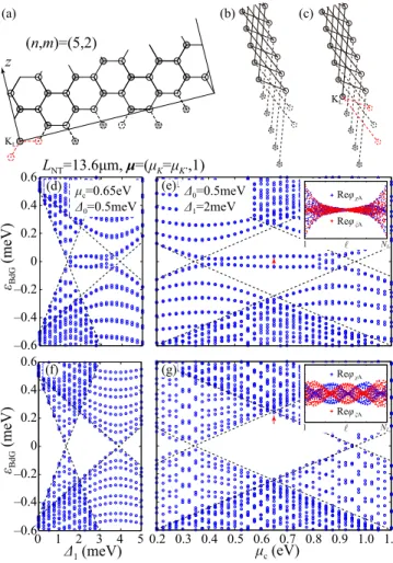
In previous studies [14,15], it has been shown that the nature of the valley coupling depends on the boundary conditions.
Here, we consider two types of boundaries. One is the minimal boundary, in which the edge has minimum number of dangling bonds [see Figs. 8(a) and 8(b)]. Another is the orthogonal
L
NT=13.6μm, μ =( μ
K= μ
K’,1)
ε
BdG(meV) 0.6 0.4
0 –0.2 –0.4 –0.6 0.2
0.3 0.4 0.5 0.6 0.7 0.8 0.9 1.0
0.2 1.1
μ
c(eV) (e)
(g)
Δ
1(meV) ε
BdG(meV)
0.6 0.4
0 –0.2 –0.4 –0.6 0.2
2
0 1 3 4 5
μ =0.65eV Δ =0.5meV
(f)
(d) Δ =0.5meV
Δ =2meV z
(a) (b) (c)
( n , m )=(5,2)
Re Re K
K
1 N
Reφ
Reφ
1 N
![TABLE I. Hopping distance δ (t j ) and phase factor δν j (t ) in the 1D lattice model [18,19]](https://thumb-eu.123doks.com/thumbv2/1library_info/3943443.1533785/3.911.85.444.133.267/table-hopping-distance-phase-factor-δν-lattice-model.webp)