Anisotropic spinrelaxation in graphene
Dissertation
zur Erlangung des Doktorgrades der Naturwissenschaften (Dr. rer. nat.)
der Fakultät für Physik an der Universität Regensburg
vorgelegt von
Sebastian Johannes Ringer
aus Geretsried
Promotionsgesuch eingereicht am: 10. Mai 2011
Die Arbeit wurde angeleitet von: Prof. Dr. Dieter Weiss
Prüfungsausschuss:
Vorsitzende: Prof. Dr. Jaroslav Fabian 1. Gutachter: Prof. Dr. Dieter Weiss
2. Gutachter: Prof. Dr. Günther Bayreuther weiterer Prüfer: Prof. Dr. Rupert Huber
Termin Promotionskolloquium: 23. Juli 2018
Contents
1 Introduction 1
2 Theoretical Background 3
2.1 Graphene . . . . 3
2.1.1 Crystal lattice . . . . 4
2.1.2 Band structure . . . . 5
2.2 Spin transport in diffusive systems . . . . 7
2.2.1 Spintronic basics - spin and spin valve . . . . 7
2.2.2 Two current model . . . . 9
2.2.3 Spin injection and relaxation . . . . 11
2.2.4 Quasichemical potentials . . . . 14
2.2.5 Spin injection efficiency: The conductivity mismatch problem . . 15
2.2.6 Non-local spin valve geometry: Johnson-Silsbee spin injection ex- periment . . . . 17
2.2.7 Spin dynamics: Hanle precession . . . . 18
2.3 Spin relaxation mechanisms in graphene . . . . 20
2.3.1 Pristine graphene: Elliott-Yafet spin relaxation . . . . 21
2.3.2 Rashba type spin-orbit fields: Dyakonov-Perel spin relaxation . . 22
2.3.3 Resonant scattering at magnetic impurities . . . . 23
2.3.4 Contact induced spin relaxation . . . . 24
2.4 How to measure the anisotropic spin relaxation in graphene . . . . 27
2.4.1 Rotating electrodes . . . . 27
2.4.2 Oblique spin precession . . . . 29
2.4.3 xHanle . . . . 32
3 Sample preparation and experimental setup 35 3.1 Graphene exfoliation . . . . 35
3.2 Lithography . . . . 39
3.3 Magnetic properties of the contacts . . . . 42
3.4 Evaporation chamber . . . . 48
3.5 Tunnel barriers made of AlO
x, MgO and TiO
x. . . . 53
3.5.1 AlO
x. . . . 55
3.5.2 MgO . . . . 59
3.5.3 TiO
x. . . . 61
3.6 Preparing a graphene spin transport device . . . . 65
3.7 Measurement setup . . . . 68
4 Experiments on anisotropic spin relaxation 73 4.1 Sample characterization . . . . 75
4.1.1 Basic sample characterization and stray fields . . . . 75
4.1.2 Magnetic orientation of the electrodes . . . . 82
4.2 xHanle measurements . . . . 87
4.2.1 Discussion of Hanle data . . . . 87
4.2.2 Fitting procedure for zHanle and xHanle . . . . 90
4.3 Oblique Spin Precession measurements . . . . 97
4.3.1 Discussion of oblique spin precession data . . . . 97
4.3.2 Oblique spin precession fitting . . . . 99
4.4 Comparison of the anisotropy parameter: Estimation of uncertainty . . . 103
4.5 Discussion . . . 107
4.6 Conclusion and outlook . . . 109
5 Spin field-effect transistor action via tunable polarization of the spin in- jection in a Co/MgO/graphene contact 111 5.1 Introduction . . . 112
5.2 Sample characterization . . . 113
5.3 Injector bias and gate dependence of the non-local spin signal . . . 116
5.4 Discussion . . . 119
5.5 Conclusion . . . 121
6 Summary 123 Appendix: Fabrication details 129 A.1 Graphene exfoliation . . . 129
A.2 Preparing AlO
xtunnel contacts . . . 133
A.3 Preparing Co electrodes with MgO tunnel contacts . . . 134
A.4 Preparing Pd circuit paths and bondpads . . . 137
Acknowledgments 139
References 141
ii
Chapter 1 Introduction
The technological advances of the past decades have largely been driven by the contin- uous rapid increase in power of micro processors. This was achieved through miniatur- ization and is described by Moore’s law, which states that the number of transistors in a dense integrated circuit doubles approximately every two years [1]. However, struc- ture sizes are approaching dimensions where in the not too distant future of 10 years, transistors based on silicon will face fundamental physical obstacles that make further miniaturization increasingly difficult if not impossible [2]. To continue the advance in microprocessor technology then requires a different approach.
One possibility is to replace silicon with a different material that has better electric properties. Graphene, a one atom thick sheet of graphite, is a potential candidate [3].
Like a semiconductor, its conductance can be manipulated by the field effect which is needed to build transistors. The improvement it offers over silicon is a much higher conductivity and charge carrier mobility, leading to faster switching circuitry that needs less power.
Another approach to advance microprocessor technology is to develop new ways to build logic circuits. Spintronics, which is a blend of the words spin and electronics, expands electronics from using only the charge of the electron to also utilizing its spin property [4]. So far, spintronic devices have only been used for data storage, but concepts exist for also building spin based logic circuitry [5–7]. As these work with magnetic switches that don’t need a constant charge refresh to keep their state, a device utilizing them would need no boot time and use considerably less power.
Spintronic devices have four basic building blocks: spin generation, spin detection, spin
transport and spin manipulation. The biggest obstacle for larger scale spintronic cir-
cuitry is the spin transport, as electron spin is fragile and short lived. In currently
used materials such as Si and GaAs, spin information decays on the length scale of mi-
crometers, which is a severe constriction for device design [8, 9]. Research effort is now
directed at getting a better understanding of the spin relaxation in materials, to then
be able to design effective countermeasures [10]. While the fundamental processes of
spin relaxation are quite well understood, the application to real world conditions are
still lacking. The problem is that spin relaxation is not a fixed material parameter but
rather a mechanism that is greatly influenced by impurities and the surroundings. The inclusion of these factors into the models is complex and the focus of current research [11–14].
When looking for long spin lifetimes and spin relaxation length, a particular material of interest is graphene [15]. It has similar features to the well known carbon nanotubes, which can be considered as rolled up graphene, but is a lot easier to fabricate. So far, graphene is the most favorable candidate for spin channel material in spin logic ap- plications [15]. As it is also suitable for regular semiconductor electronics, this opens the possibility of hybrid designs on a single material. This powerful combination gives graphene great potential as a candidate to replace silicon in the next generation of mi- croprocessor technology.
However, graphene is also a prime example to demonstrate the limits of the current models of spin relaxation. Based on the spin orbit interaction, which is the basic source for most spin relaxation processes, graphene should have a spin lifetime upwards of 50 ns [16]. This is three orders of magnitude higher than the 100 ps that were actually mea- sured in the first experiments [17]. The difference can be attributed to invasive effects of the contacts, impurities and the substrate. Since then, researchers have been trying to properly model these invasive effects and have been somewhat successful in mitigating them [18]. Although progress has been made, the question which is the dominant spin relaxation mechanism in graphene is still not solved. The motivation to find an answer is high, as that would allow to design effective countermeasures and perform experiments with record breaking spin lifetimes.
The focus of this work is the study of the spin relaxation processes in graphene. Par- ticularly, the experiments focus on a precise measurement of the anisotropy parameter of the spin relaxation, which can be used to identify the different proposed relaxation mechanisms [19, 20]. Several models exist that at least give results for the spin lifetime that match the experiment. What is missing however, is to unambiguously identify a proposed mechanism by also matching its other characteristics like the spin lifetime anisotropy and the energy dependence. So far, what is the limiting factor for the spin lifetime in graphene is still open for debate.
The second part of this work is the report of a newly discovered property of a Co/M- gO/graphene tunnel contact, where the spin polarization of the tunnel current can be tuned and even inverted by the applied current bias and back gate voltage. By using this contact in a non-local spin valve geometry, spin transistor action is demonstrated where the transistor is switched on or off by a back gate that controls the spin injection.
2
Chapter 2
Theoretical Background
2.1 Graphene
Graphite consists of layers of carbon atoms in a hexagonal lattice. If the graphite is so thin that is has just a few of these layers, it is called graphene. The graphene is then differentiated by the number of layers it has and is accordingly called single layer graphene, bilayer graphene, trilayer graphene etc. When it is called just graphene, usu- ally the single layer variant is meant.
The name „graphene“ was coined by Hanns-Peter Boehm et al. [21], who were the first to observe it in 1961 [22]. Although graphene has unintentionally been produced over the centuries through the use of pencils, the challenge is to isolate it. Boehm, who had studied chemistry in Regensburg from 1947 to 1951 [23], obtained graphene through the reduction of graphite oxide. He then used a „Siemens Übermikroskop 100 e“, an early commercial TEM, to measure the thickness of the obtained thin carbon films. With the method of graphite oxide reduction, the graphene sheets are first in solution and when placed on a substrate will be crumpled and full of wrinkles. As the article of Boehm et al.
mostly just stated that atomically thin graphite films exist and are thermodynamically stable (a disputed fact up to that point), it did not gather much attention. What was missing were measurements hinting at the extraordinary properties of this material.
Graphene was then largely forgotten until 2004, when Konstantin Novoselov and An- dre Geim published an article in Science titled „Electric field effect in atomically thin carbon films“ [24]. They obtained high quality, wrinkle free single layer graphene by mechanical exfoliation (repeated peeling) of a graphite block with scotch tape. Their article demonstrated that graphene has multiple electric properties (2DEG, electric field effect, ballistic transport) that were previously very hard or impossible to obtain in other materials. As their method to fabricate graphene was cheap, reliable and easy to copy, this animated research groups worldwide to also start experimenting with the material.
The response in the science community was so huge that K. Novoselov and A. Geim
were awarded the 2010 Nobel prize for enabling this development. Since then, the study
of graphene has revealed so many record breaking properties that is must be called a
wonder material. A review article in Science by A. Geim states:
Graphene is a wonder material with many superlatives to its name. It is the thinnest known material in the universe and the strongest ever mea- sured. Its charge carriers exhibit giant intrinsic mobility, have zero effective mass, and can travel for micrometers without scattering at room tempera- ture. Graphene can sustain current densities six orders of magnitude higher than that of copper, shows record thermal conductivity and stiffness, is im- permeable to gases, and reconciles such conflicting qualities as brittleness and ductility. Electron transport in graphene is described by a Dirac-like equation, which allows the investigation of relativistic quantum phenomena in a benchtop experiment. [25]
2.1.1 Crystal lattice
The unique properties of graphene arise from its crystal structure. In the hexagonal graphene lattice, each carbon atom is about a = 1.42Å from its three neighbors [28].
The ground state electronic configuration of carbon is 1s
22s
22p
2, with single electrons in two of the three 2p orbitals and one unoccupied 2p orbital [29]. To form more than two bonds, one of the 2s electrons is promoted to the free 2p orbital, resulting in four unpaired electrons. In graphene, the remaining 2s electron hybridizes with two of the 2p orbitals to form three sp
2hybrid orbitals. These are located in the graphene plane and form a strong σ bond with each neighbor [30]. The σ bonds are responsible for the
Figure 2.1: Left: Graphene lattice, depicting the diamond shaped unit cell containing two carbon atoms marked A (blue) and B (gray). Adapted from [26]. Right: Brillouin zone of graphene, showing the location of the K and K
0points. Adapted from [27].
4
superb mechanical stability of graphene.
The remaining p orbital is oriented out-of-plane and forms π bonds with its neighbors.
Like in benzene rings, these π bonds are delocalised and the resulting electronic band- structure is half filled. The π bonds are responsible for the electric properties of graphene [26].
The honeycomb lattice of graphene can be described as a hexagonal Bravais lattice with a diamond shaped unit cell containing two atoms, as shown in Fig. 2.1. The two atoms are both carbon, but in the lattice their properties are not identical. Each atom forms a sub lattice in the Bravais lattice, named A and B in Fig. 2.1 [29].
2.1.2 Band structure
The π bonds of the carbon atoms hybridize to form π- and π∗-bands. The π-band is the valence band while the π∗-band is the conduction band. They touch only at the K and K
0points of the Brillouin zone (see Fig. 2.1), but do not overlap [26]. These points are called Dirac points, because of the unique properties of the band structure in these spots. The existence of two K points arises from the two atoms in the unit cell of the Bravais lattice.
The Fermi level lies at the Dirac point and here the density of states (DOS) is zero. This makes graphene a zero-gap semiconductor. The energy dispersion at the Dirac point and thus at the Fermi level is linear [29]:
E
±(~k) = ±v
F~ |~k| (2.1)
This formula is valid for both K and K
0. The energy E is the difference of energy to the Fermi level, ~k is the wave vector originating from the K or K
0point, ~ is the reduced
Figure 2.2: Electric dispersion of graphene, with a zoom in of the energy bands close to the
Dirac points. Adapted from [27].
Figure 2.3: Ambipolar field effect in graphene, resulting in the typi- cal Dirac curve of the graphene sheet resistance when changing the charge carrier concentration in graphene with a gate. The sketches of the Dirac cones show the Fermi level and the corresponding charge carrier type. Adapted from [31].
Planck constant and v
Fis the Fermi velocity. The full dispersion relation of graphene is depicted in Fig. 2.2, with a zoom of the Dirac cone that is a result of the linear energy dispersion at the Dirac point described by equation 2.1.
A consequence of this linear dispersion relation is that both electrons and holes have a constant velocity that is independent of their energy. As they can not be accelerated by increasing their energy, they have infinite effective mass. The Hamiltonian describing these particles at the Dirac point is equivalent to a Dirac Hamiltonian for massless fermions, with the speed of light substituted by the Fermi velocity in graphene v
F≈
300c[26]. The word „Dirac point“ was coined by this similarity.
Calculating the DOS for the band structure at the Dirac point reveals a linear energy dependency: [27]
ν(E) = g
sg
v2π
|E|
~
2v
F2(2.2)
Here, g
srepresents the degeneracy due to the spin degree of freedom and g
vrepresents the degeneracy due to the valley degree of freedom that arises from the K and K
0points.
As the field effect can be used to change the charge carrier concentration in graphene, the DOS can easily be observed experimentally. The usual setup for this is to exfoliate graphene on a Si/SiO
2silicon chip, where the SiO
2is the isolating top layer. The Si underneath is highly doped and serves as a back gate. Measuring the graphene sheet resistance while sweeping the back gate will result in the graph shown in Fig. 2.3.
Applying a gate voltage will move the Fermi level up or down in the Dirac cone. The charge carrier concentration n changes accordingly, resulting in a different sheet resis- tance R
sq= (neµ)
−1, where µ is the electron mobility and e the electron charge [32].
When the Fermi level is at the Dirac point, there are very few charge carriers and the resistance is highest. Moving the Fermi level in any direction away from the Dirac point
6
will symmetrically lower the resistance. This measurement can be used to extract the electron mobility µ in graphene.
According to the formula, R
sqshould be infinity when the Fermi level is at the Dirac point, as there are no states there. However, measurements show that graphene has a minimum conductivity [32, 33], which is referred to as quantum-limited resistivity [29].
2.2 Spin transport in diffusive systems
2.2.1 Spintronic basics - spin and spin valve
Spintronics expands electronics from only using the charge of the electron to also using its spin property [4]. The spin of an electron is a quantum mechanical state that is called „spin“ because its mathematical description has similarities to the angular mo- mentum of a spinning object. To obtain the spin quantum number, the spin vector is compared against a quantization axis. For the electron, this will return „points in the same direction“ (spin up) or „does not point in the same direction“ (spin down). If the quantization axis is inverted, the result will be exactly opposite.
The spin gives electrons a magnetic moment, similar to the magnetic dipole created when an electrically charged object is spinning [34]. As a result of this magnetic dipole, the electron spin interacts with a magnetic field. The spin vector will precess around a magnetic field and over time relax into a parallel (spin up) or antiparallel (spin down) orientation.
Because of this interaction with magnetism, ferromagnets (FM) play a central role in spintronic applications. While in a regular metal (N) the spin of an electron is irrele- vant to its conductance, in an FM spin up and spin down experience different electrical resistances [35]. The electric current flowing in a FM is dominated by the spins with the higher conductance, which is called a current spin polarization. Current flowing from a FM to a N material will keep this spin polarization for some time, effectively injecting the spin polarization into the N material [36]. Depending on the FM material, the orien- tation of the injected spin is either parallel or antiparallel to its magnetization direction.
The orientation of the spins injected into N can then be controlled by manipulating the magnetization of the FM.
When it is the other way around and a spin polarized current flows into a FM, the
FM acts as a spin detector [36]. The current will have the least resistance if the high
conductance spin state in the FM is aligned with the majority spins of the current. By
having current flow through two FM in series, this creates a so called spin valve, where
the resistance is low for a parallel orientation of the two FM and high for an antiparalell
orientation. This is schematically shown in Fig. 2.4. This device utilizes the vector
property of the spin, demonstrating the enhanced functionality that spintronics offers
over regular electronics.
Figure 2.4: Schematic function of a spin valve. In the parallel orientation, the spin up electrons can pass through both ferromagnets unhindered while the spin down electrons experience a high resistance. In the antiparallel orientation, the spin up electrons become spin down electrons and vice versa in the second ferromagnet. Now both spin channels experience a high resistance in one of the magnets and the overall resistance is higher than in the parallel state.
A spin valve is not the only possible spintronic device, but so far it is the most successful one [37]. Several types of spin valves exist. The spin valve depicted in Fig. 2.4 is based on the giant magnetoresistive effect (GMR). Actual devices consist of two thin magnetic layers, separated by a thin nonmagnetic layer. The non-magnetic layer in between is needed to decouple the magnetization of the magnetic layers.
The commercial success of spintronics started with spin valves based on the GMR effect.
The GMR effect was discovered in 1988 simultaneously by Albert Fert and Peter Grün- berg [38, 39], who were awarded the 2007 nobel Prize for its discovery. A remarkable fact about the GMR effect is that it only took 10 years from the discovery until commercial products were available. Stuart Parkin perfected GMR devices for IBM so they could be used as hyper sensitive magnetic field sensors [37]. These were then used in hard disk read heads, which enabled a huge leap in hard disk storage capacity from 1.6 GB per platter in 1996 (Quantum Fireball ST) to 5.6 GB per platter in 1998 (IBM Deskstar 16GP).
The function of a GMR spin valve device seems simple enough that the question must be asked why this was not discovered sooner. The reason is spin flip processes and spin relaxation. The spin valve effect as depicted in Fig. 2.4 depends on the electrons keeping their spin state between the first and the second FM. Electron spin is generally short-lived and fragile, the time electrons stay in one spin state is usually in the order of pico seconds. Depending on which material is used as a spacer, the two FM need to have a separation of just a few nanometers to still work as a spin valve [37]. For larger distances, the effect is nullified by spin relaxation.
8
2.2.2 Two current model
In the experiments presented in this work, a spin polarization in graphene is created by spin injection from a FM. The mathematics to describe the related spin phenomena employ a two current model that was established by Mott et al [40]. This model is based on the conductance in FMs, where spin up and spin down have a separate density of states (DOS) and can be treated as if flowing in different conductors. The model is valid when the chance of a spin flip during a scattering event is small, so that the coupling between the spin channels is weak.
For the following definitions, the index ↑ signifies spin up while ↓ signifies spin down.
The nomenclature is according to J. Fabian et al. [35].
Electron density: n = n
↑+ n
↓(2.3)
Spin density: s = n
↑− n
↓(2.4)
Density polarization: P
n= n
↑− n
↓n
↑+ n
↓= s
n (2.5)
The spin density s is defined as the difference between spin up and spin down electron density, it is the density of spins that have no counterpart. The density polarization P
ndescribes the fraction of electrons that have a spin without counterpart. When the term ’spin’ is used as in „spin is injected into graphene“, what is meant by ’spin’ is the parameter s of electrons at the Fermi level. When it is further stated that „the injected spins create a spin polarization in graphene“, the term ’spin polarization’ refers to the parameter P
nof electrons at the Fermi level in graphene.
As spin is a vector, the question must be asked how that is represented in this two current model. In a FM where the spins align parallel or antiparallel to the magnetization, any other orientation of spin gets projected onto this axis. Spins perpendicular to the magnetization are treated as if unpolarized (mapped to 50% spin up + 50% spin down).
In an N material where there is no preferred direction for the spin, the spin density is a vector with the three components s
x, s
yand s
z:
~ s =
s
xs
ys
z
(2.6)
A spin density of any orientation is then treated as a linear combination of spin density s
x, s
yand s
zon the x, y and z axis, respectively.
In section 2.2.1 it was stated that the current flowing in a FM is spin polarized. This
is because in a FM, the electronic bands for spin up and spin down are shifted relative
to each other as shown in Fig. 2.5. As a result, at the Fermi level there is a difference
between n
↑and n
↓in equilibrium and current flowing in a FM is spin polarized. The
Figure 2.5: DOS at the Fermi level E
Fof a nonmagnetic conductor (N, left), in this case n- doped graphene, and a ferromagnetic conductor (FM, right). In N there is an equal number of spin up and spin down electrons in equilibrium. In the FM, the densities are different due to the exchange splitting causing the minima of the two spin bands to be displaced. The spin of the larger electronic density is called majority spin; the spin of the smaller density is called minority spin. However, usually the density of states at the Fermi level is higher for the minority than for the majority electrons. Adapted from [35].
formula for the spin polarization in equilibrium P
0is then [35]:
P
0=
g
↑− g
↓g
↑+ g
↓(2.7) With g
↑and g
↓being the density of states at the Fermi level for spin up and spin down electrons, respectively. Graphene as a nonmagnetic material has the same density of states for spin up and spin down electrons and thus no spin polarization in equilibrium.
It should be noted that for the spin polarization in general there is no simple formula, as that is affected by temperature, the electronic band structure, electric fields, chemical potentials, doping, etc [35]. Formula 2.7 for P
0is a simplification as it lacks a temper- ature dependence. Some materials like cobalt have an insignificant variation of P
0with temperature, so for cobalt this formula is quite accurate. Other materials like permalloy have a stronger variation of P
0with temperature and require a different formula [41].
The difference in conductance for spin up and spin down in a FM also originates from the spin split DOS. In general, the conductivity σ of a material is described by the Einstein relation [35]:
σ = e
2Dg (2.8)
Here, D is the charge carrier diffusion coefficient, e is the electron charge and g = g
↑+ g
↓is the density of states at the Fermi level. In a FM where the DOS is spin dependent, σ then needs to be calculated separately for each spin state:
σ
↑= e
2D
↑g
↑, σ
↓= e
2D
↓g
↓(2.9)
The diffusivity D is then also spin dependent.
10
2.2.3 Spin injection and relaxation
When doing spin injection with a FM/N junction, we seek an answer to the following question:
Given the equilibrium spin polarization P
0in the ferromagnet, what is the spin accumulation in the nonmagnetic conductor if electric current j flows through the junction?[36]
The word ’spin accumulation’ signifies the difference of the spin polarization to the equilibrium state. In the N material this is equivalent to the spin polarization, but ’ac- cumulation’ is a better description of the situation.
The spin polarized current coming from the FM creates a spin density s at the N side of the FM/N interface. This spin density propagates in N by drift and diffusion, but is also subject to spin relaxation. The spin polarization in the N material is highest at the FM/N interface, the spin ’accumulates’ there. This is shown in Fig. 2.6.
The spin accumulation in N is a static out of equilibrium state that is reached as a balance of spin source and spin drain. The spin source is the current j through the FM/N junction. We discuss a one dimensional model, so the current j is equivalent to the current density. The particle current (density) is then j/(−e). The number of unpaired spins arriving in N per unit of time would then be j
s0/(−e), with the spin current [36]:
j
s0= P
0j (2.10)
This is a rough estimate of what to expect but neglects several things. Spin also accu- mulates in the FM which increases the junction resistance (spin bottleneck effect) [35].
Depending on the relative electrical resistances of the FM and N region, a spin polar- ization in the FM might not matter when the resistance of the N region is much higher than the resistance of the FM (conductivity mismatch problem, see section 2.2.5). We also assumed that the spin is conserved when crossing the interface, which is actually a good approximation [35].
Note that j
s06= 0 is achieved for both current directions. When the current flows into the FM this is called spin extraction. The current in the FM is carried by the majority spins at the Fermi level, so these will be the ones that predominantly enter the FM. The minority spins will be left behind in the N, where they are now in the majority as spins of the other type are extracted into the FM.
The spin sinks in N that counteract a spin accumulation from the spin injection are spin diffusion, spin drift and spin relaxation. These are described by the drift diffusion equation for the spin density s(x, t) [35]:
∂s
∂t = D ∂
2s
∂x
2− µ
eE ∂s
∂x − s
τ
s(2.11)
Figure 2.6: (a) Creating a spin accumulation in a non magnetic conductor (N) by means of spin injection from a ferromagnet (FM). Left: Spin dependent DOS of the FM. Middle:
DOS of N, in this case n-doped graphene, with a spin accumulation. Right: DOS of N in equilibrium. (b) The spin accumulation s(x) in N decays as a function of the position x with the spin relaxation length L
s. Adapted from [42].
12
This formula does not account for spin precession and is only valid for B = 0. On the right hand side, the first term describes diffusion with the diffusion coefficient D. The second term describes drift with the electron mobility µ
eand the electric field E, the product of which equals the drift velocity v
d. The electron mobility µ
eis written here with index e to avoid confusion with the quasichemical potential µ that will be intro- duced in the next section. The last term on the right hand side describes spin relaxation with the spin relaxation time τ
s. Note that equation 2.11 is strictly speaking just for the one dimensional case, but under the right circumstances can also be used for 2D or 3D.
The experiments in this work use the non-local spin valve geometry that can create a purely diffusive spin current without drift (see section 2.2.6). When the spin accumu- lation has reached an equilibrium and the system can be considered in a steady state (∂s/∂t = 0), the equation for the N region is then reduced to [35]:
0 = D ∂
2s
∂x
2− s
τ
s(2.12)
This is then rearranged to:
∂
2s
∂x
2= s
Dτ
s= s
L
s2(2.13)
With the spin relaxation length L
s= √
Dτ
s. Using the boundary condition that the spin density vanishes at infinity s(∞) = 0, the solution for s in the interval of (0, ∞) is then:
s(x) = s
x=0e
−x/Ls(2.14) So the spin accumulation at the FM/N interface s
x=0decays in N exponentially and L
sis the length after which the spin density has dropped by a factor of 1/e. The mechanisms that cause the spin relaxation are discussed in section 2.3.
The influence of the N region on the spin accumulation s
x=0can now be calculated by specifying the spin source. We use the non-local geometry as an example, were a spin current j
s,nlenters the N region at x = 0 only by diffusion [36]:
j
s,nl(x = 0) = eD ∂s
∂x
x=0(2.15) The differential equation for j
s,nlis another boundary condition that must be fulfilled by s(x) and we get:
s(x) = j
s,nl−e L
sD e
−x/Ls(2.16)
The spin density at x = 0 is now
s(0) = j
s,nl−e L
sD (2.17)
The spin accumulation at the FM/N interface on the N side is dependent not only on the
spin current j
s,nlflowing into N but also on the properties of N. The spin accumulation
is higher for a long spin relaxation length (slow spin relaxation), while a high diffusivity
D lowers the spin accumulation (the spins disperse faster).
2.2.4 Quasichemical potentials
In the model described so far, electrons and therefore spin move through either drift or diffusion. As the result of these two forces is the same (the electron is moving), drift and diffusion can be combined into a single parameter called the quasichemical potential µ. To find out what force is acting on an electron, it is then sufficient to look at the gradient of the quasichemical potential. With the conductivity σ, the electrical current can then be written as [35]:
j = σ∇µ (2.18)
As was already shown in Fig. 2.6, each spin state can have a separate quasichemical potential µ
↑and µ
↓. The individual spin currents are then:
j
↑= σ
↑∇µ
↑(2.19)
j
↓= σ
↓∇µ
↓(2.20)
For σ and µ, spin dependent parameters can be defined:
σ = σ
↑+ σ
↓, σ
s= σ
↑− σ
↓(2.21)
µ = 1
2 (µ
↑+ µ
↓), µ
s= 1
2 (µ
↑− µ
↓) (2.22)
As was seen in Fig. 2.6, a spin accumulation leads to µ
↑6= µ
↓and therefore µ
s6= 0.
Because of this, the spin quasichemical potential µ
sis also called a spin accumulation.
These definitions can now be used to formulate equations for the charge current j and spin current j
sbased on the quasichemical potentials and conductivities [35]:
j = j
↑+ j
↓= σ∇µ + σ
s∇µ
s(2.23) j
s= j
↑− j
↓= σ
s∇µ + σ∇µ
s(2.24) These equations allow for an easy description of several situations. In a nonmagnetic conductor σ
s= 0 (no difference in spin up and spin down conductivities), so j is decou- pled from j
s. A spin current j
sis driven only by the gradient of the spin accumulation µ
sand can be present without a charge current j. This is then a pure spin current where spin up electrons move in one direction while an equal number of spin down electrons move in the opposite direction. The spin density is changing without changing the elec- trical charge.
In a ferromagnet σ
s6= 0, the different spin channels have different conductivities. As a consequence of that, a gradient in the spin accumulation µ
scan create an electrical current while a gradient of the quasichemical potential µ can create a spin current.
The relationship between spin density s and spin quasichemical potential µ
sis [35]:
δs = s − s
0= 4eµ
sg
↑g
↓g (2.25)
14
With s
0the spin density in equilibrium. As can be seen, the non equilibrium spin density δs is proportional to the spin quasichemical potential µ
sand both can be called a spin accumulation. In a normal conductor where s
0= 0 and g
↑= g
↓=
12g, equation 2.25 can be simplified to s = eµ
sg. This is the number of electron states in the interval of eµ
sat the Fermi level.
2.2.5 Spin injection efficiency: The conductivity mismatch problem
In section 2.2.3 we have assumed that the spin current j
sentering N at a FM/N junction through spin injection is simply j
s= P
0j, with P
0the spin polarization of the FM. It was already stated that this omits several effects that are present at a FM/N junction. Using the introduced formalism of quasichemical potentials allows a more accurate description of the problem, which is called the standard model of electrical spin injection [35, 43].
The first addition is to expand the FM/N junction to FM/C/N, to additionally in- clude the contact C at x = 0 into the calculation. The generalized current polarization P
j= j
s/j is then modeled using µ and µ
sfor each region FM, C and N. To solve the system, it is assumed that P
jmust be continuous across the interface [36]:
P
j= P
jF M(0) = P
jN(0) = P
jC(2.26) Since the contact region C is defined as a single point at x = 0, the quasichemical potential µ is allowed to have a discontinuity there. The current polarization P
jacross the interface can then be expressed as a function of the effective resistances R
F M, R
Cand R
Nof the FM, C and N region, respectively, and the conductivity spin polarization P
σF M= σ
s/σ of the FM region and P
Σof the C region [36]:
P
j≡ R
F MP
σF M+ R
cP
ΣR
F M+ R
c+ R
N= hP
σi
R(2.27) This P
jis then called the spin injection efficiency. Qualitatively, P
jis the conductivity spin polarization averaged over the three regions hP
σi, weighted by the effective resis- tances.
The conductivity spin polarization P
Σof the contact is not a material parameter. It would make sense in case of a tunnel contact when there is actually a material between FM and N, but not for a direct FM/N contact. P
Σmust be understood as a parameter depending on both FM and N. The best example would be a tunnel contact, where the tunneling probability according to Fermi’s golden rule is proportional to the density of states g on both sides. In the FM g
↑6= g
↓, so the tunneling probability, which is equivalent to the conductivity, is different for spin up and spin down. This difference in conductivity is then expressed by P
Σ.
Equation 2.27 can now be used to explain the conductivity mismatch problem that was
first discussed by Schmidt et al. [44]. The essence of the problem is that the spin injec-
tion efficiency P
jdepends on the conductivities (resistances) of the FM and N material.
Figure 2.7: The equivalent circuit diagram to explain the conductivity mismatch problem, in a) for a FM/N junction with R
N> R
F Mand in b) with an additional tunnel barrier R
C. In a) the resistance in both spin channels is dominated by R
Nand the resulting spin polarization in N is very low. In b) the resistance is dominated by the spin dependent R
C, resulting in a much better spin polarization in N.
In the case of a direct FM/N contact with low contact resistance, R
CR
F M, R
N. Equation 2.27 is then reduced to:
P
j= R
F MR
F M+ R
NP
σF M(2.28)
As can be seen, the injected current P
jretains most of the spin polarization P
σF Mof the FM if the resistance of the N material R
Nis lower or of the same order of magnitude as R
F M. In the case of Co as the FM and graphene as N however, R
N> R
F Mand the spin injection efficiency is severely reduced. The problem is most prominent when spin injection into a semiconductor is attempted (R
NR
F M).
The conductivity mismatch problem can be reduced or circumvented when the contact resistance is artificially increased, for example by introducing a tunnel barrier. In the case of R
CR
F M, R
N, equation 2.27 is reduced to:
P
j≈ P
Σ(2.29)
As has been stated before, P
Σstill depends on the FM and N material.
The conductivity mismatch problem can be qualitatively explained by looking at the equivalent circuit diagram in Fig. 2.7. For a direct FM/N contact shown in Fig. 2.7a) with R
N> R
F M, the resistance in each spin channel is dominated by R
N. The difference in resistance of R
F M↑and R
F M↓does not change the total resistance much. When a high resistance tunnel contact is inserted between FM and N as shown in Fig. 2.7b), the resistance in each spin channel is dominated by R
C↑and R
C↓. Then the current flowing in N has a much higher spin polarization.
16
2.2.6 Non-local spin valve geometry: Johnson-Silsbee spin injection experiment
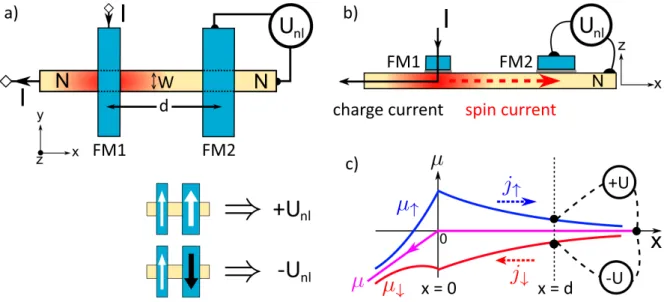
When studying spin transport in a material, the most popular setup to do so is the non-local spin valve geometry shown in Fig. 2.8, established by M. Johnson and R. H.
Silsbee [46]. The major benefit of this setup is that it creates a pure spin current that propagates by diffusion, excluding the spurious effects of the charge current in a regular (local) spin valve setup.
The principle of the non-local spin valve geometry is to separate the injector circuit from the detector circuit. The spin channel then needs to have four contacts, two for the injector circuit and two for the detector circuit. In Fig. 2.8, the injector circuit is connected to FM1 and the left end of the N spin channel. When a current is applied to inject spins under FM1, the electric field that causes the electron drift in N is confined to the left side of FM1. The region of N that is to the right of FM1, called the non-local region, is then free of an electric field and electron drift. This is an accurate description when a 2D material like graphene is used as a spin channel. For thicker 3D spin channels, there may still be spurious effects of the injector current in the non-local region [47].
A spin accumulation is created under FM1 by spin injection. Through electron diffusion driven by the quasichemical potential, a pure spin current propagates to the right of FM1 into the non-local region. There is no charge current, as a spin up electron moving in one
Figure 2.8: Sketch of the lateral non-local spin valve geometry in a) top view and b) side view.
A spin accumulation (red) is created under FM1 by spin injection, the charge current I is flowing towards the left end of the spin channel. On the right side of FM1, a pure spin current propagates by diffusion to contact FM2, where it is detected as the non-local voltage U
nl. c) Display of the corresponding quasichemical potentials µ, µ
↑and µ
↓in the spin channel. For a P orientation of FM1 and FM2 U
nlis positive, while for an AP orientation U
nlis negative.
Adapted from [45].
direction is counterbalanced by a spin down electron moving in the opposite direction.
The spin accumulation in the non-local region can be detected by the detector circuit, which consists of FM2 and a non magnetic reference electrode at the right end of the spin channel. Because of the so called „Silsbee-Johnson spin-charge coupling“ [48], a spin accumulation µ
sat the FM2/N interface will result in a non-local voltage U
nlproportional to µ
sin the open detector circuit.
With the applied current I
injat the injector circuit, the non-local voltage U
nlis then [42]:
U
nl= ±I
injP
injP
detR
sqL
s2W e
−d/Ls(2.30)
Here, P
injand P
detare the spin injection efficiencies of FM1 and FM2, respectively.
R
sq= 1/σ is the sheet resistance of N, W is the width of the spin channel, d is the distance between the centers of FM1 and FM2 and L
sis the spin relaxation length in N.
When reporting experimental results, it is common practice to not state U
nlbut rather the non-local resistance R
nl= U
nl/I
inj.
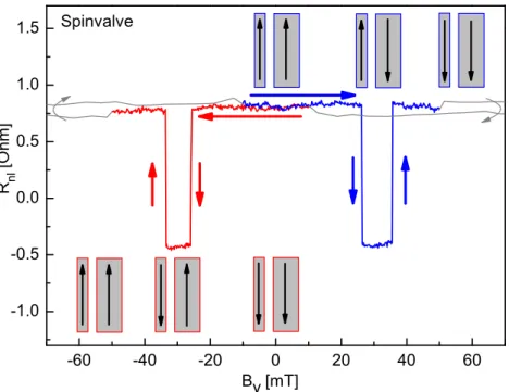
The ’±’ in equation 2.30 is for parallel and antiparallel orientation of FM1 and FM2. If the orientation of ~ s is not P or AP to the magnetization in FM2, ~ s is projected onto that magnetization and the signal strength is reduced accordingly. This happens for instance during Hanle measurements and can be used to probe the orientation of ~ s.
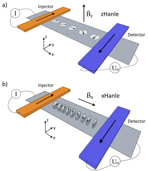
2.2.7 Spin dynamics: Hanle precession
The standard method to to measure the spin relaxation time τ
sof a spin channel in a non-local spin valve setup is a Hanle measurement, depicted in Fig. 2.9a). Here, a magnetic field B ~ is applied perpendicular to the direction of the injected spins, usually the z direction as shown in Fig. 2.9a). The spins then precess around the magnetic field while diffusing from injector to detector. The orientation the spins have when they reach the detector is now dependent on their travel time and the strength of the magnetic field. By performing a magnetic sweep in both P and AP configuration, one obtains the non-local resistance R
nlwith the characteristic Hanle oscillations as shown in Fig. 2.9c). By fitting the traces, the spin relaxation time τ
scan be extracted.
For a mathematical description of the effect, the diffusion equation for the spin density
~ s is expanded to also include spin precession ~ s × ~ ω, with the Larmor frequency ω ~
0= γ ~ B and the gyromagnetic ratio γ. [35]:
∂~ s
∂t = ~ s × ~ ω + D ∂
2~ s
∂x
2− ~ s
τ
s(2.31)
Note that the diffusion equation now needs to be calculated with ~ s as a vector, but the equation is still for a 1D model. For the orientation of electrodes and magnetic field as shown in Fig. 2.9a), the solution to this equation that is used to fit the Hanle oscillations is:
R
nl= U
nlI
inj= ± P
injP
detR
sqD W
Z
∞ 0dt 1
√ 4πDt e
−d2/4Dte
−t/τscos(ω
0t) (2.32)
18
The „±“ is to account for P or AP alignment of the electrodes. For B = 0, this formula is identical to equation 2.30. If the electrodes are not parallel or antiparallel, this solution is not valid.
Formula 2.32 consists of four parts. The prefactor in front of the integral is responsible for the height of the central peak at B = 0. If it is sufficient to only extract τ
s, the prefactor can be ignored and the normalized data fitted with a normalized function.
The term
√14πDt
e
−d2/4Dtis a (gaussian) probability distribution, which represents the spacial profile of diffusing particles. The term e
−t/τsis the spin relaxation. The final term cos(ω
0t) is the projection of the spin vector onto the magnetization axis (with ω
0= | ω ~
0|), which changes over time because of Larmor precession.
Figure 2.9: a) Sketch of a Hanle measurement in a non-local spin valve geometry. b) Projection
of the spin vector onto the magnetization axis which changes over time due to Larmor
precession, for P and AP orientation. c) Normalized Hanle oscillations in the non-local
resistance R
nl, obtained by performing magnet sweeps in P and AP orientation. b) and c)
adapted from [42].
2.3 Spin relaxation mechanisms in graphene
Spin-orbit interaction is the source of various spin relaxation and dephasing mechanisms.
The interaction is a relativistic effect that results from the electrons moving in the elec- tric field of the positively charged nuclei. In the electron’s frame of reference, the nuclei are moving and produce a magnetic field that the electron spin interacts with. The strength of the interaction scales with the charge of the nuclei. For graphene, which is entirely made of carbon atoms, the spin-orbit interaction is very weak compared to other materials as carbon has just six protons [49, 50].
As a result, graphene should have very long spin-lifetimes and would be an ideal can- didate for a spin channel in spintronic applications [15, 51]. Based on the spin-orbit interaction, calculations predict a spin lifetime exceeding 50 ns [16]. However, experi- ments up to now could only measure spin-lifetimes of a few nanoseconds [52–54]. Because of this discrepancy between calculation and experiment, it is apparent that the model the calculation is based on (perfectly flat, defect free graphene in vacuum) is of limited use. Since then, there has been an ongoing discussion of what additional spin relaxation mechanisms exist in graphene that are limiting the measured spin-lifetimes. Several sources for additional spin relaxation in graphene have been proposed [15]: impurities (adatoms) [55], the substrate [56], polymer residues [57–59], ripples[60], resonant mag- netic scattering at magnetic impurities [11, 61] and contact induced spin relaxation [62–
64].
In a real world sample it is expected to have several of these relaxation mechanisms at once, which increases the difficulty of identifying them. Each mechanism has an associ- ated relaxation rate τ, and they are added to a total spin relaxation rate τ
totalaccording to this formula:
1
τ
total= 1 τ
1+ 1
τ
2+ . . . (2.33)
To determine which is the dominant effect, experiments focused on finding a correlation between the momentum scattering time τ
pof electrons and their spin relaxation time τ
s[65–67]. This would allow to differentiate between Elliott-Yafet type scattering, where τ
s∼ τ
p, and Dyakonov-Perel type scattering, where τ
s∼ 1/τ
p. This approach has so far produced no conclusive results [15].
Figure 2.10: In graphene, the relaxation rate of the spins can depend on their orientation. Spins that are oriented in plane experience τ
xywhile spins oriented out of plane experience τ
z.
20
Another signature of spin relaxation mechanisms is the anisotropy or isotropy of the spin relaxation time. The out-of-plane spin relaxation time, which we will call τ
z, can be different from the in-plane spin relaxation time, which we will call τ
xy(see Fig. 2.10).
For convenience, we introduce ζ :=
ττzxy
![Figure 2.15: The change in τ s f it and D f it fitted for different d/L s as a function of R/L s [(a) and (c)] and for different R/L s as a function of d/L s [(b) and (d)]](https://thumb-eu.123doks.com/thumbv2/1library_info/3853040.1516186/29.892.170.747.419.959/figure-change-τ-fitted-different-function-different-function.webp)