www.pss-rapid.com
pss
Identification of excitons, trions and biexcitons in single-layer WS
2Gerd Plechinger, Philipp Nagler, Julia Kraus, Nicola Paradiso, Christoph Strunk, Christian Schüller, and Tobias Korn*
Institut für Experimentelle und Angewandte Physik, Universität Regensburg, 93040 Regensburg, Germany Received 8 July 2015, revised 22 July 2015, accepted 23 July 2015
Published online 27 July 2015
Keywords dichalcogenides, WS2, photoluminescence, excitons, trions, biexcitons, direct-gap semiconductors
* Corresponding author: e-mail tobias.korn@physik.uni-regensburg.de, Phone: +49-941-9432055, Fax: +49-941-9434226
© 2015 WILEY-VCH Verlag GmbH & Co. KGaA, Weinheim
1 Introduction In recent years, semiconducting, atomically thin transition metal dichalcogenides (TMDCs) like MoS2, MoSe2, WSe2 and WS2, have emerged as highly interesting materials for the scientific community due to their extraordinary optical [1] and electrical properties [2], including coupled spin–valley effects [3] and photovoltaic applications [4]. These molecular layers show strong pho- toluminescence (PL) peaks in the visible and near-infrared spectral range, as they experience a transition from an indi- rect gap in bulk and few-layer samples to a direct gap in the single-layer regime [5]. The spatial confinement of car- riers in a two-dimensional layer and the weak dielectric screening lead to unusually strong excitonic effects [6, 7], even at room temperature. High exciton binding energies of the order of 0.5 eV have been reported for single-layer WS2 [8–11]. Besides the charge-neutral exciton (X), i.e., a bound state of an electron and a hole, also charged excitons can be excited in the presence of residual excess charge carriers. These quasiparticles, called trions, consist either of two electrons and one hole (X–) or one electron and two holes (X+). By applying a gate voltage, one can tune the spectral weight of charge-neutral excitons and trions in single-layer MoS2 [12], MoSe2 [13], WS2 [10] and WSe2
[14]. Additional, lower-energy PL emission peaks are ob- served in most single-layer TMDCs at low temperatures.
These have been attributed to surface-adsorbate-bound ex- citons in MoS2 [15] and to crystal-defect-bound exciton
states in single-layer diselenides [16, 17]. Given the large binding energy of the excitons, the formation of molecular states consisting of two excitons, so-called biexcitons [18], is to be expected in dichalcogenide single-layers. Biexciton PL emission should be at energies below the exciton emis- sion due to the additional binding energy, in a similar en- ergy range as defect-bound exciton emission. The signa- ture of biexciton emission was recently observed in PL measurements on WSe2 [19]. Thus, the origin of the lower- energy PL emission peaks in the other semiconducting TMDCs warrants close investigation.
In this work, we report on low-temperature PL of me- chanically exfoliated single-layer WS2. To date, only a few works exist which report on the observation of excitons and trions in the low-temperature PL spectrum of me- chanically exfoliated [20, 21] single-layer WS2. To the best of our knowledge, a thorough analysis of the temperature- dependent PL spectrum is still absent. In contrast to other semiconducting TMDCs, there is no consensus about the assignment of the X and X– PL features in low-temperature PL of single-layer WS2. The aim of this paper is to clarify those issues, and to provide insight into the nature of an additional low-energy peak in the PL spectrum, which is observable at low temperatures. We identify the exciton and the trion peaks in the temperature range from 295 K to 4 K. Our interpretation of the PL spectra is substantiated by gate-dependent PL measurements which allow us to di- Single-layer WS2 is a direct-gap semiconductor showing
strong excitonic photoluminescence features in the visible spectral range. Here, we present temperature-dependent pho- toluminescence measurements on mechanically exfoliated single-layer WS2, revealing the existence of neutral and charged excitons at low temperatures as well as at room tem-
perature. By applying a gate voltage, we can electrically con- trol the ratio of excitons and trions and assert a residual n- type doping of our samples. At high excitation densities and low temperatures, an additional peak at energies below the trion dominates the photoluminescence, which we identify as biexciton emission.
rectly control the exciton–trion ratio. Finally, we utilize power-dependent and helicity-resolved PL measurements to show that the low-energy PL peak we observe stems from a superposition of defect-bound exciton and biexciton emission.
2 Methods Our samples are mechanically exfoliated from bulk WS2 crystals (2d semiconductors inc.) onto a polydimethylsiloxane (PDMS) stamp. Using an optical microscope, we can identify single-layer flakes of WS2 on the PDMS stamp. We then transfer these flakes onto a p-doped Si chip with a 270 nm SiO2 capping layer, apply- ing an all-dry deterministic transfer procedure [22]. For gate-dependent measurements, we stamp the flakes onto p-doped Si chips with 500 nm thermal oxide and pre- defined metal contacts manufactured with e-beam litho- graphy. We use the p-doped Si as a backgate. For low- temperature measurements, the samples are mounted in a He-flow cryostat. The cw lasers used for excitation are focussed with a 100× microscope objective onto the sam- ple, the emitted PL is collected by the same microscope objective (backscattering geometry) and guided into a spectrometer with a Peltier-cooled CCD chip. Unless otherwise noted, a 532 nm laser source is utilized. Helicity- resolved measurements are performed using a 561 nm laser, which allows for near-resonant excitation. Further experi- mental details are published in Ref. [23].
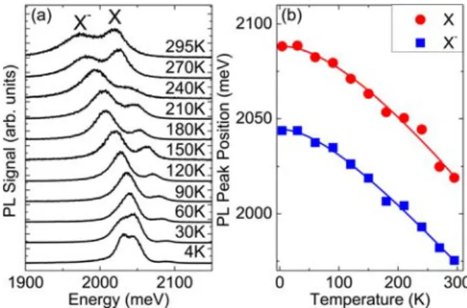
3 Results and discussion Figure 1(a) shows the PL spectra of single-layer WS2 for various temperatures. In this measurement series, the laser excitation density is kept relatively low at 5 kWcm–2 to avoid possible heating effects. At 295 K, the spectrumconsists of two peaks at 2018 meV and 1975 meV, which we attribute to the exci- ton (X) and the trion (X–). The peak positions at room temperature are in very good agreement with recent reports [10, 24, 25]. We note that even at room temperature, X and X– peaks can be separated due to their small linewidth. The
Figure 1 (a) Normalized PL spectra of single-layer WS2 for dif- ferent temperatures. (b) Exciton (X) and trion (X–) PL peak ener- gies as a function of temperature. The solid lines represent the fits to the experimental data following the Varshni equation.
existence of the trion peak indicates an intrinsic doping of our sample, as it is commonly observed also in other TMDCs [2]. When cooling down the sample, both PL peaks experience a blueshift in accordance with the Varshni equation [26], which describes the change of the bandgap with temperature in a large variety of semicon- ductors,
2
g( ) g(0) /( ) ,
E T =E -αT T+β (1)
where Eg(0) is the bandgap at zero temperature and α and β are phenomenological fit parameters. We assume that the exciton and trion binding energy are temperature-inde- pendent, and that X and X– peaks rigidly shift with the bandgap. We use Eq. (1) to fit the PL peak positions extracted for each temperature, as depicted in Fig. 1(b).
For both peaks, the fit matches with α = . ¥4 0 10-4eV/K, β = 200 K and Eg(0) 2088= meV for X and Eg(0)= 2045 meV for X–. The parameters are comparable to those from previous studies on MoS2 [27]. Our assignment of the X and X- peaks at T = 4 K is further confirmed by addi- tional power-dependent PL measurements at 150 K [28], in which we observe a low-energy tail in the X– peak, which is typical of an electron-recoil effect and has recently also been observed for trions in MoSe2 [13]. The spectral weight shifts from X to X– with decreasing temperature.
This indicates that the thermal energy at higher tempera- tures is large enough to lead to a partial dissociation of the trions. In Fig. 1(a), we also see that the X– peak develops a low-energy shoulder at 30 K and, even more pronounced, at 4 K, which we denominate as L1/XX. We will demon- strate below that it stems from a superposition of defect- bound exciton (L1) and biexciton (XX) emission. In previ- ous reports, either the L1 and L2 peak [21] or the X– and L1
peak [20, 29], have been attributed to exciton and trion emission. The actual X peak at about 2.09 eV is absent in those studies. The fact that we see a well-pronounced exci- ton peak in our spectra might be due to our sample prepa- ration process, which leads to a reduced interaction with the substrate in comparison to direct exfoliation of flakes onto SiO2 using adhesive tape.
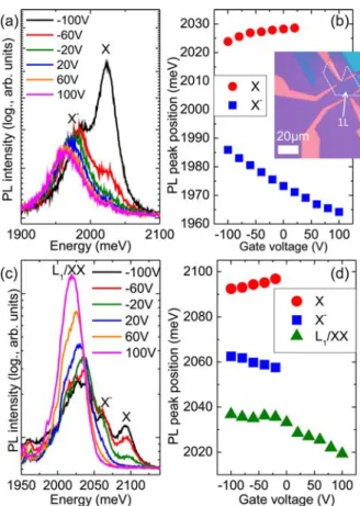
To confirm our assignment of the exciton and trion peaks, as well as the charge state of the trion, we perform gate-dependent PL measurements. The inset in Fig. 2(b) shows a microscope image of a gated sample. In Fig. 2(a), PL spectra are plotted for different backgate voltages Vg at room temperature. At large negative Vg, the X peak is the dominant one, whereas it is completely suppressed for positive Vg, where the X– peak is the only measurable fea- ture. Hence, we infer that the trions in our samples are negatively charged. This indicates that the WS2 single- layer has a residual n-type doping, similar to MoS2 [2] but in contrast to WSe2 [30]. Our room-temperature data is in perfect agreement with Ref. [10]. Figure 2(c) displays the gate-dependent PL spectra at 4 K. For negative gate volt- ages, the X peak intensity increases as the Fermi level is shifted towards the neutral regime. This clearly confirms
Figure 2 (a) PL spectra at room temperature for different gate voltages. (b) PL peak position of X and X– as a function of gate voltage. The inset shows an optical micrograph of the WS2 flake on a Si/SiO2 substrate with prestructured Ti:Au contacts. (c) PL spectra at T = 4 K for different gate voltages. (d) PL peak position of X, X– and L1/XX peak as a function of gate voltage.
the identification of the 2.088 eV peak as the exciton peak.
The X– peak, in contrast, gains in intensity by increasing the gate voltage for Vg >0. In both gate-voltage dependent measurement series, we observe that the X– peak experien- ces a spectral redshift, while the X peak shows a slight blueshift with increasing Vg (Fig. 2(b) and (d)), so that the energy difference between X and X- peaks increases with increasing carrier concentration. This effect has also been observed in other TMDCs [12, 13]. In the limit of low car- rier concentration, the ionization energy of a trion is equal to the trion binding energy.In the presence of a 2D electron gas (2DEG), however, ionization of a trion requires that the ionized electron is excited to a state above the Fermi energy of the 2DEG, as all states below the Fermi energy are occupied. Thus, the energy difference between exciton and trion peaks is given by [12]
X X b X F,
E -E - =E, - +E (2)
with EX and EX- being the exciton and trion PL peak en- ergies, Eb,X– the trion binding energy and EF the Fermi en- ergy, which is proportional to Vg. Due to intrinsic doping and the corresponding non-zero EF, the measured exciton-
trion energy difference EX-EX- of 43 meV in the un- gated sample shown in Fig. 1(a) is larger than the actual trion binding energy. The exciton-trion peak separation in gated samples follows Eq. (2) [28], showing a minimal peak separation of 30 meV at Vg = -100 V. This repre- sents an upper limit for the trion binding energy.
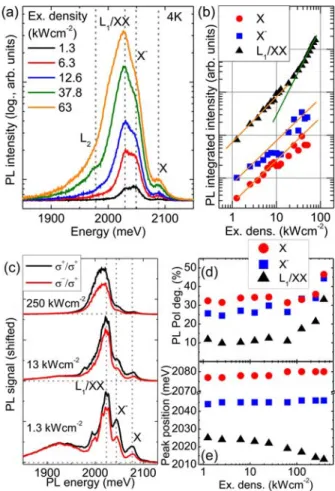
Finally, we focus on the low-energy feature labeled as L1/XX that arises at temperatures below 60 K. Figure 3(a) shows the PL spectra at T = 4 K for different excitation powers. Whereas at low powers, X- and L1/XX are spec- trally well separated and of similar intensity, at higher ex- citation powers, the L1/XX peak completely dominates the spectrum. Additionally, a second low-energy peak L2 with moderate intensity is discernible around 1.98 eV. It may stem from defect-bound excitons, as its intensity decreases relative to the other peaks with increasing excitation den- sity. To get a better insight into the nature of the L1/XX peak, we extract the integrated PL intensity for L1/XX, X– and X for different excitation densities, as displayed in the double-logarithmic graph in Fig. 3(b). X and X- show a rather linear behavior indicated by the orange solid line, as expected for an excitonic feature [18]. In contrast, the L1/XX peak exhibits a linear dependence at low excitation density, while for excitation densities larger than 25 kWcm–2, the data is well-described by a quadratic fit, indicated by the green solid line in Fig. 3(b). Such a quad- ratic increase in PL emission intensity is expected for biex- citons [31], although smaller, superlinear slopes are often observed in experiment due to the kinetics of biexciton for- mation and exciton recombination [19]. The different be- havior for low and high excitation densities indicates that in fact, two different emission lines are responsible for the observed L1/XX peak: at low excitation density, the main contribution to the PL at the L1/XX peak position stems from defect-bound excitons (denominated L1). At high ex- citation density, the biexciton (XX) emission is dominant.
To confirm our interpretation, we perform an excitation- density dependent measurement series utilizing near- resonant, circularly-polarized excitation. Figure 3(c) shows helicity-resolved PL spectra measured at 4 K using differ- ent excitation densities. At low excitation density, L1/XX, X– and X peaks are clearly observable, together with a spectrally broad feature at lower energy. This feature is reminiscent of low-temperature PL spectra of MoS2, where it is attributed to surface-adsorbate-bound excitons [15].
For this feature, co- and contra-circularly-polarized PL spectra have the same intensity, indicating no circular po- larization. By contrast, L1/XX, X– and X peaks show a clear intensity difference in the helicity-resolved PL. With increasing excitation density, the L1/XX emission begins to dominate the spectrum. For higher excitation densities, in the same range for which we observe the quadratic in- crease of the PL intensity discussed above, the L1/XX peak position shows a pronounced redshift and its polarization degree increases. These two observations are analyzed and compared to the behavior of the X– and X peaks in Fig. 3(d) and (e). The circular polarization degree of the
Figure 3 (a) PL spectra of single-layer WS2 at T = 4 K for vari- ous excitation densities. (b) Double-logarithmic plot of integrated PL intensity of X (red circles), X– (blue squares) and L1/XX peak (black triangles) as a function of excitation density. The orange solid lines indicate a linear dependency, whereas the green solid line indicates a quadratic dependency. (c) Helicity-resolved PL spectra of single-layer WS2 at T = 4 K under near-resonant, circu- larly-polarized excitation for various excitation densities. The black and red spectra are for co-circular and contra-circular exci- tation and detection, respectively. (d) PL circular polarization de- gree and (e) PL peak position for X, X– and L1/XX peaks as a function of excitation density.
PL emission in single-layer TMDCs is an indicator of valley polarization, and for defect-related PL peaks, low values have been reported. By contrast, excitons, trions and biexcitons should show a significant PL polarization degree under near-resonant excitation [19]. In Fig. 3(d), we show that the PL polarization for the X– and X peaks is high and remains almost constant throughout the investi- gated excitation density range. By contrast, the L1/XX peak has a low PL polarization degree at low excitation density, indicative of defect-related PL emission. The PL polarization degree increases with increasing excitation density,as expected for biexciton emission, reaching simi- lar values as the X– peak for the highest excitation density values in our series. As shown in Fig. 3(e), the L1/XX peak redshifts by about 10 meV in the investigated excitation density range. This indicates that the L1 emission from de-
fect-bound excitons at low excitation density is at a higher energy than the biexciton emission at high excitation den- sity. We exclude local heating induced by the laser as a source of the redshift for the L1/XX, since neither X– or X peaks display a redshift – by contrast, they show a slight blueshift. Thus, we can interpret the energy separation of about 65 meV between the X and XX features as the bi- exciton binding energy Eb XX, .Currently, the value of the exciton binding energy in single-layer WS2 is still under discussion. The values determined in different experiments range between 320 meV [8] and 700 meV [9]. Thus, the Haynes factor, i.e., the ratio of Eb XX, and the exciton bind- ing energy, ranges between 9 and 20 percent, which is comparable to values for biexcitons in quantum wells [18]
and those observed in WSe2 [19]. Remarkably, in our WS2
samples, strong biexciton PL emission is observable al- ready under cw laser excitation, while pulsed excitation was required to study biexciton emission in WSe2 [19].
This indicates pronounced differences in the kinetics of biexciton formation in different TMDCs.
4 Conclusion In conclusion, we have presented temperature-dependent PL measurements on mechanically exfoliated single-layer WS2. We find that the exciton and trion peaks are well separated even in the room tempera- ture spectrum and their emission can be tracked downto 4 K. By tuning the Fermi level in our samples, we can un- ambiguously assign the 2.09 eV PL peak to exciton and the 2.05 eV PL peak to trion emission at T = 4 K. At low tem- peratures, we observe the emergence of a lower-energy peak, which we identify as a superposition of defect-bound exciton and biexciton emission by the power dependence of its emission intensity and circular polarization degree.
These results clarify some issues in the interpretation of low-temperature PL spectra in single-layer WS2, which is a promising candidate for all-2D electrooptical and valley- tronic devices.
Acknowledgements The authors ackowledge financial support by the DFG via KO3612/1-1, GRK1570 and SFB689.
Supporting Information Additional supporting informa- tion may be found in the online version of this article at the pub- lisher’s website.
References
[1] K. F. Mak, C. Lee, J. Hone, J. Shan, and T. F. Heinz, Phys.
Rev. Lett. 105, 136805 (2010).
[2] B. Radisavljevic, A. Radenovic, J. Brivio, V. Giacometti, and A. Kis, Nature Nanotechnol. 6, 147–150 (2011).
[3] K. F. Mak, K. He, J. Shan, and T. F. Heinz, Nature Nanotechnol. 7, 494–498 (2012).
[4] M. M. Furchi, A. Pospischil, F. Libisch, J. Burgdörfer, and T. Mueller, Nano Lett. 14, 4785–4791 (2014).
[5] A. Splendiani, L. Sun, Y. Zhang, T. Li, J. Kim, C. Y. Chim, G. Galli, and F. Wang, Nano Lett. 10, 1271–1275 (2010).
[6] T. Cheiwchanchamnangij and W. R. L. Lambrecht, Phys.
Rev. B 85, 205302 (2012).
[7] G. Berghäuser and E. Malic, Phys. Rev. B 89, 125309 (2014).
[8] A. Chernikov, T. C. Berkelbach, H. M. Hill, A. Rigosi, Y. Li, O. B. Aslan, D. R. Reichman, M. S. Hybertsen, and T. F. Heinz, Phys. Rev. Lett. 113, 076802 (2014).
[9] Z. Ye, T. Cao, K. O’Brien, H. Zhu, X. Yin, Y. Wang, S. G.
Louie, and X. Zhang, Nature 513, 214–218 (2014).
[10] B. Zhu, X. Chen, and X. Cui, Sci. Rep. 5, 9218 (2015).
[11] A. T. Hanbicki, M. Currie, G. Kioseoglou, A. L. Friedman, and B. T. Jonker, Solid State Commun. 203, 16–20 (2015).
[12] K. F. Mak, K. He, C. Lee, G. H. Lee, J. Hone, T. F. Heinz, and J. Shan, Nature Mater. 12, 207–211 (2013).
[13] J. S. Ross, S. F. Wu, H. Y. Yu, N. J. Ghimire, A. M. Jones, G. Aivazian, J. Q. Yan, D. G. Mandrus, D. Xiao, W. Yao, and X. Xu, Nature Commun. 4, 1474 (2013).
[14] A. M. Jones, H. Yu, N. J. Ghimire, S. Wu, G. Aivazian, J. S.
Ross, B. Zhao, J. Yan, D. G. Mandrus, D. Xiao, W. Yao, and X. Xu, Nature Nanotechnol. 8, 634–638 (2013).
[15] G. Plechinger, F. X. Schrettenbrunner, J. Eroms, D. Weiss, C. Schüller, and T. Korn, Phys. Status Solidi RRL 6, 126–
128 (2012).
[16] G. Wang, L. Bouet, D. Lagarde, M. Vidal, A. Balocchi, T. Amand, X. Marie, and B. Urbaszek, Phys. Rev. B 90, 075413 (2014).
[17] G. Wang, L. Bouet, D. Lagarde, M. Vidal, A. Balocchi, T.
Amand, X. Marie, and B. Urbaszek, Phys. Rev. B 90, 075413 (2014).
[18] C. F. Klingshirn (ed.), Semiconductor Optics (Springer, 2007).
[19] Y. You, X. X. Zhang, T. C. Berkelbach, M. S. Hybertsen, D. R. Reichman, and T. F. Heinz, Nature Phys. 11, 477–481 (2015).
[20] T. Scrace, Y. Tsai, B. Barman, L. Scheidenback, A. Petrou, G. Kioseoglou, I. Ozfidan, M. Korkusinski, and P. Hawry- lak, Nature Nanotechnol. (2015), 2015/05/11/online.
[21] A. A. Mitioglu, P. Plochocka, J. N. Jadczak, W. Escoffier, G. L. J. A. Rikken, L. Kulyuk, and D. K. Maude, Phys. Rev.
B 88, 245403 (2013).
[22] A. Castellanos-Gomez, M. Buscema, R. Molendaar, V. Singh, L. Janssen, H. S. J. van der Zant, and G. A. Steele, 2D Ma- terials 1, 011002 (2014).
[23] G. Plechinger, J. Mann, E. Preciado, D. Barroso, A. Ngu- yen, J. Eroms, C. Schüller, L. Bartels, and T. Korn, Semi- cond. Sci. Technol. 29, 064008 (2014).
[24] N. Peimyoo, W. Yang, J. Shang, X. Shen, Y. Wang, and T. Yu, ACS Nano 8, 11320–11329 (2014).
[25] M. Z. Bellus, F. Ceballos, H. Y. Chiu, and H. Zhao, ACS Nano 9(6), 6459–6464 (2015).
[26] Y. Varshni, Physica 34, 149 (1967).
[27] T. Korn, S. Heydrich, M. Hirmer, J. Schmutzler, and C. Schüller, Appl. Phys. Lett. 99, 102109 (2011).
[28] See Supplementary Information for further details.
[29] Y. Ye, Z. J. Wong, X. Lu, H. Zhu, X. Chen, Y. Wang, and X. Zhang, arXiv:1503.06141 (2015).
[30] C. H. Lee, G. H. Lee, A. M. van der Zande, W. Chen, Y. Li, M. Han, X. Cui, G. Arefe, C. Nuckolls, T. F. Heinz, J. Guo, J. Hone, and P. Kim, Nature Nanotechnol. 9, 676–681 (2014).
[31] P. L. Gourley and J. P. Wolfe, Phys. Rev. B 20, 3319–3327 (1979).