Ab initio spin-flip conductance of hydrogenated graphene nanoribbons:
Spin-orbit interaction and scattering with local impurity spins
Jan Wilhelm,1,2,*Michael Walz,1,2and Ferdinand Evers3
1Institute of Nanotechnology, Karlsruhe Institute of Technology, D-76344 Eggenstein-Leopoldshafen, Germany
2Institut f¨ur Theorie der Kondensierten Materie, Karlsruhe Institute of Technology, D-76128 Karlsruhe, Germany
3Institute for Theoretical Physics, University of Regensburg, D-93040 Regensburg, Germany (Received 9 April 2015; published 6 July 2015)
We calculate the spin-dependent zero-bias conductanceGσ σin armchair graphene nanoribbons with hydrogen adsorbates employing a DFT-basedab initiotransport formalism including spin-orbit interaction. We find that the spin-flip conductanceGσσ¯ can reach the same order of magnitude as the spin-conserving oneGσ σ, due to exchange-mediated spin scattering. In contrast, the genuine spin-orbit interaction appears to play a secondary role, only.
DOI:10.1103/PhysRevB.92.014405 PACS number(s): 72.80.Rj,72.25.Dc,73.63.Nm
I. INTRODUCTION
In recent years, graphene [1] has been considered as ideal spintronics material [2]: Due to the weak spin-orbit interaction (SOI) [3], spin lifetimes of Dirac electrons are expected to be long. However, the Hanle precession measurements typically yield spin diffusion times several orders of magnitude below the theoretical predictions [4]. Recently, a quantum interference measurement [5] proposed that intrinsic local magnetic moments at defects [6] are the primary cause of spin relaxation in graphene, masking any potential effects of the genuine SOI. The efficiency of such a mechanism was confirmed by consecutive theoretical work for single-layer graphene [7] and recently, also for bilayer graphene [8].
While another mechanism for spin-flips originating from bias induced orbital magnetism has also been identified, recently, its quantitative effect still remains to be explored [9].
Motivated by the rich spin physics in graphene, we study spin-dependent transport in graphene nanoribbons (GNRs), i.e., strips of graphene with ultrathin width, from first princi- ples. Our interest in GNRs is closely related to their electronic properties: GNRs inherit a weak intrinsic SOI [10] and high electron mobility from graphene [11]. Moreover, GNRs exhibit gaps that can be tuned with the ribbon width [12,13] and local spins can be generated at zigzag edges [14–17] or defects [6].
These properties make GNRs promising materials for appli- cations in spintronics, e.g., for quantum computing [18].
Spin transport in GNRs will be addressed in this paper using the standard formalism of molecular electronics [19]: A device scattering region is located between two semi-infinite leads with applied biasV; the total conductanceG=dI /dV of the device is split into four spin-dependent conductance coefficientsGσ σ(withG=
σ σGσ σ). They account for an electronic current being injected with spinσ, and, after passing the device region, measured with spin directionσ.
In ribbons with spin-degenerate electronic structure and neglected spin-flip scattering, G splits equally, G↑↑=G/2 andG↓↓=G/2 [20–25]. In the case of magnetic ribbons,↑
*Present address: Department of Chemistry, University of Zurich, Winterthurerstrasse 190, CH-8057 Zurich, Switzerland;
jan.wilhelm@chem.uzh.ch
and↓current do not match anymore; unpaired spins in the ribbon, e.g., at defects or zigzag edges, can cause characteristic differences betweenG↑↑andG↓↓[26–31].
The spin-flip conductance coefficients G↑↓ andG↓↑ are nonvanishing in the presence of (i) SOI [32–39] or (ii) exchange interaction with local spins in the device [40]. To include SOI in our DFT formalism, we employ an all-electron SOI module [41], the exchange-interaction is dealt with on the level of spin DFT [42]; details see Sec.II.
As one would expect, we find a very small spin-flip conductanceGσσ¯ in clean armchair GNRs (AGNRs) due to the very weak SOI and the absence of local impurity spins, see Sec.III A. In contrast, the spin-flip conductance is massively enhanced in the presence of adsorbates, see Secs.III B–III D.
For instance, our results indicate that the spin-flip probability associated with a single hydrogen adatom can be comparable to the spin-conserving one. This high spin-flip probability is rationalized by employing a simplistic tight-binding (toy) model. Our first-principles results are qualitatively similar to analytical results by earlier authors [7] who employ a model calculation that is valid in the highly dilute limit.
II. METHOD
In our calculations we are employing an extension of the AITRANSS platform, our DFT-based transport simulation tool [43–47]. The spin-dependent conductance is obtained as follows: We extract the Kohn-Sham (KS) Hamiltonian Hˆ=[( ˆH↑↑,Hˆ↑↓),( ˆH↓↑,Hˆ↓↓)], a 2×2 block-matrix in spin space, from a DFT calculation [48] including all-electron SOI [41] for a finite-size hydrogen-terminated graphene nanoribbon with horizontal armchair edges, see Fig.1. Sub- sequently we obtain the (retarded) single particle KS-Green’s function ˆG of a finite-size strip in the presence of the left and right contacts by standard recursive Green’s function techniques [19]:
G(E)ˆ ≡
Gˆ↑↑ Gˆ↑↓
Gˆ↓↑ Gˆ↓↓
=
Gˆ−10 −ˆL−ˆR−1 . (1) The spin-diagonal self-energies ˆα=[( ˆ↑α,0),(0,ˆ↓α)] with ˆ↑α=ˆ↓αreflect the presence of the leads [49]. They are treated with a closed-shell electronic structure and a vanishing SOI
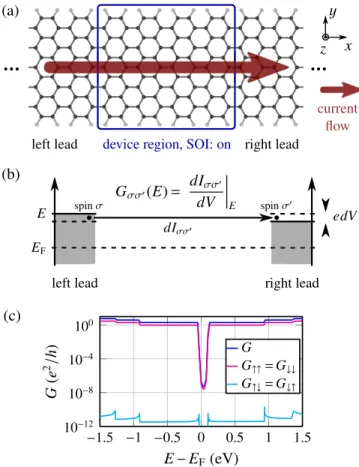
FIG. 1. (Color online) (a) Structure of the clean AGNR11 device.
In the blue marked device region, SOI is present. (b) Between the two leads of (a), an infinitesimal voltage dV is applied. As response, an electronic currentdI flows, which is split into four components dIσ σ. They account for an electronic current being injected with spin σ and measured after passing the device region with spinσ. The spin-dependent conductanceGσ σ(E) at a given chemical potential Eis then defined as a ratio ofdIσ σ anddV. The reference energy EFis the chemical potential of the isolated, charge-neutral device.
(c) Corresponding conductance of the pristine ribbon (a) according to Eq. (2). The spin quantization axis is chosen in positivezdirection.
The spin-flip conductanceGσσ¯ is nonvanishing due to SOI. The spin- conserving conductance does not vanish completely inside the band gap (but is reduced by seven orders of magnitude) due to the limited length of the lead system inx direction. This is a methodological artifact that reflects a small numerical difference between the exact lead-induced self-energy and our approximation scheme (decimation technique [47]).
so that spin is a good quantum number in the leads [50].
Gˆ0 represents the bare KS-Green’s function of the device region, see Fig.1(a). We compute the spin-dependent zero-bias conductance Gσ σ(E) at a given chemical potential E [see Fig.1(b)] in a Landauer-B¨uttiker approach [51,52]:
Gσ σ(E)=e2 h Tr
ˆLσ( ˆGσ σ)†ˆRσGˆσσ
, (2)
with ˆσα=i[ ˆσα−( ˆσα)†].
For spin quantization n=(sinθcosϕ,sinθsinϕ,cosθ) deviating from default z direction, we rotate the Green’s
function in spin space by the unitary transformU:
Gˆ(n) =UGUˆ †, U =
cosθ2 −e−iϕsinθ2 eiϕsinθ2 cosθ2
. (3) Due to the closed-shell electronic structure of the leads, ˆσα remains unchanged by a unitary transform and the conductance with respect to an arbitrary spin quantization axisnis given by
G(n)σ σ(E)=e2 h Tr
ˆLσGˆ(n)σ σ
†
ˆRσGˆ(n)σσ
. (4)
The formalism outlined here is well established [32–39].
III. RESULTS
In this section we present simulation results of the spin- dependent conductance Gσ σ of clean and hydrogenated AGNRs calculated according to Eqs. (2) and (4). For com- putational details we refer to AppendixA.
A. Clean ribbon
We calculate the conductance coefficientsGσ σ(E) of an AGNR withNC=11 transverse carbon atoms (AGNR11), see Fig.1(a)for the molecular structure of the device and Fig.1(b) for a sketch of the electronic structure and the transport setup.
The result for the spin-dependent conductance according to Eq. (2) is shown in Fig. 1(c) with a spin quantization axis in the +z direction. For the spin-conserving conductance coefficientsGσ σ, we find a step function withGσ σ(E)/(e2/ h) simply counting the energy bands intersecting with a given energyE [53,54].Gσ σ is hardly affected by the SOI. Most importantly, the spin-flip conductance is found to be very small with an upper bound of 10−10e2/ hdue to the very weak SOI as expected [55]. Due to vertical mirror symmetry,↑zand↓z
bands of pristine AGNRs are degenerate [56] and therefore G↑↑(E)=G↓↓(E) andG↑↓(E)=G↓↑(E) forzquantization.
B. Ribbon with a single hydrogen adatom
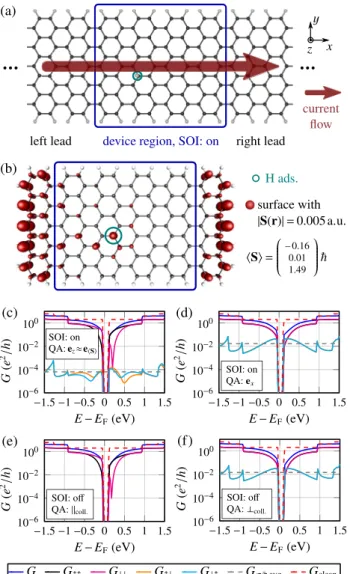
We continue with a ribbon containing a single hydrogen adatom, see Fig.2(a)for the molecular geometry. Hydrogen forms a chemical bond with the underlying carbon atom resulting in an sp3 hybridization. The four nearest carbon atoms were structurally relaxed in order to catch the massive enhancement of SOI due to the lattice distortion [57–60].
First, we comment on the finite-size DFT calculation of the ribbon including SOI as sketched in Fig. 2(b):
The computed magnetization of the finite-size ribbon is S =(−0.16,−0.01,1.49)T[61], so there are approximately three unpaired electrons in the ribbon distributed at the zigzag edges [14–16] and near the impurity, see Fig.2(b)[62].
Our simulation results for the spin-dependent conductance Gσ σaccording to Eqs. (2) and (4) are displayed in Figs.2(c)–
2(f). First, we focus on the situation where the average magnetic moment of sample and incoming electrons are (very nearly) aligned which we refer to as collinear case throughout the paper. The corresponding spin-conserving conductance Gσ σ is displayed in Fig. 2(c) with SOI and Fig.2(e)without SOI. The values forG↑↑(E) andG↓↓(E) in Figs.2(c)and2(e)deviate by less than 10−2e2/ h, only, and we
FIG. 2. (Color online) (a) Structure of the AGNR11 device with one single hydrogen adsorbate. (b) Finite-size ribbon for the un- derlying DFT calculation including SOI. All atoms in the blue box belong to the device region. The red surface denotes the isosurface of the spin densityS(r) calculated by the DFT including SOI where we observe the famous zigzag edge magnetism [14–17]. The total spin is calculated as S = S(r)d3r. (c)–(f) Conductance of the device (a) with/without SOI and quantization axis (QA) according to the inset: (c) Collinear case [average magnetization of the sample and spin of incoming electrons are (very nearly) aligned] with SOI, (d) noncollinear case (spin polarization axis of incoming electrons and average magnetization axis of local impurity spins are perpendicular) with SOI, (e) collinear case without SOI, and (f) noncollinear case without SOI. The reference energyEF is the chemical potential of the isolated, charge-neutral lead. The average spin-flip conductance Gσσ ,avg¯ is computed as arithmetic mean ofG↑↓(E) andG↓↑(E) in the energy interval [−1.5 eV,1.5 eV]. Gclean(E) denotes the total conductance of the pristine ribbon.
observe that SOI hardly influencesGσ σ. In particular, the broad antiresonance [63–77] indicating the quasilocalized state (zero mode) that accompanies the isolated adatom remains clearly visible also in the presence of SOI. In Fig.2(c)the spin-flip conductance is seen to be very small, Gσσ¯(E)∼10−4e2/ h, while it vanishes in Fig.2(e)due to the absence of SOI.
Next, we consider in Fig. 2(d) incoming electrons with spin polarization along thex axis, i.e., perpendicular to the axis ≈ez of the average local impurity spins in the ribbon which we callnoncollinear casethroughout the paper. Here the spin-flip conductance increases strongly reaching values larger than 0.05e2/ h. Near the band gap it is even exceeding the spin-conserving conductance. In order to emphasize that the large spin-flip conductance is due to the exchange interaction and not related to SOI, we repeat the same calculation without SOI. The result is shown in Fig.2(f) and indeed it is indistinguishable from Fig.2(d).
In a nutshell, the exchange-driven spin flip is understood as follows [78]: Say the fixed impurity spin points into thezdirec- tion, i.e., the exchange interaction turns intoSimpz Sˆcondz ∼σˆcondz with the Pauli matrix ˆσcondz acting on incoming conduction electrons. As a consequence, the effective single-particle Hamiltonian no longer commutes with ˆσcondx,y. Hence, the spin of the incoming particles no longer is conserved, if it happens to exhibit a component perpendicular to the impurity spin. Therefore, spin-flips become possible with a probability (G↑↓+G↓↑)/
σ σGσ σ that can reach order unity for a noncollinear spin passing a single hydrogen adatom.
In AppendixBwe explain how our results are rationalized employing a simple toy model. Our overall findings are consistent with Ref. [7] that has employed a model calculation.
C. Ribbon with two hydrogen adatoms
We calculate the spin-dependent conductance of a ribbon with two neighboring hydrogen adatoms, see Fig.3(a). This double-hydrogen defect is nonmagnetic and we would like to confront it with the case of an isolated hydrogen adatom.
In Fig. 3(a) the nonmagnetic character of this impurity is evident: The spin density near the impurity is smaller than
FIG. 3. (Color online) (a) Finite-size ribbon with two hydrogen adatoms for the underlying DFT calculation including SOI. The atomic structure is relaxed including the six surrounding carbon atoms. All atoms in the blue box belong to the device region.
(b) Spin-dependent conductance for z-polarized electrons and (c) forx-polarized electrons. All symbols are defined in the caption of Fig.2.
the isovalue and so it cannot be resolved anymore. There are two reasons for the absence of magnetism with this defect.
(i) There is no imbalance between the graphene sublattices, i.e., one impurity on each sublattice. This also implies that the number of electrons remains even. (ii) Because of the vicinity of the border, orbital degeneracies are lifted, so that a closed-shell ground state is favored.
The computed conductance is shown in Fig.3(b) for the collinear case and in Fig.3(c)for the noncollinear one. Indeed, the spin-flip conductance for noncollinear transport is two orders of magnitude smaller as compared to the previous case with a single hydrogen adatom. Note that again the spin-flip conductance for electrons polarized perpendicular to the sample magnetization exceeds the collinear one—
probably due to weak residual magnetism with spin density
|S(r)|<0.005 a.u.
We conclude that the interactions between hydrogen adatoms can be relevant if they come sufficiently close. In our example, the spin-flip conductance of the ribbon with two hydrogen adatoms is far less than twice the value of the isolated adatom. This indicates a breakdown of Matthiesen’s rule in the limit of higher concentrations.
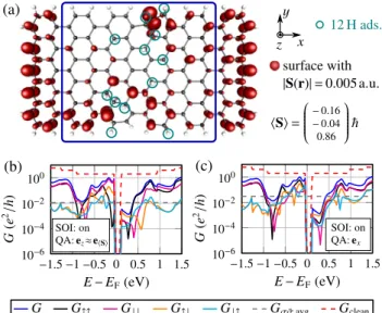
D. Massively hydrogenated ribbon
In Fig.4 we show the spin-dependent conductance for a ribbon with 12 adsorbed hydrogen atoms which are distributed randomly on the ribbon. The part of the structure that carries 44 carbon atoms and 12 adsorbed hydrogen atoms was structurally relaxed. The transmission function displayed in Figs. 4(b) and 4(c) is seen to carry strong mesoscopic fluctuations that reflect many quasilocalized states near the Fermi energy. In this situation, the spin-flip conductance can reach the same order of magnitude as the spin-conserving one in a sizable energy window.
FIG. 4. (Color online) (a) Finite-size ribbon with 12 hydrogen adatoms for the underlying DFT calculation including SOI. The total number of unpaired electrons isNSpin=2/|S| =1.75. All atoms in the blue box belong to the device region. (b) Spin-dependent conductance for electrons polarized alongezand (c) forxpolarization.
All symbols are defined in the caption of Fig.2.
FIG. 5. (Color online) Local current density response (integrated over the out-of-plane direction; normalized to the conductance per width) in the hydrogenated AGNR11 shown in Fig.4(a)(blue box only). The current density exhibits strong mesoscopic fluctuations that reflect in a logarithmic color scale covering three decades. Some interesting current paths are drawn into the picture for illustration:
Local current vortices exceeding the spatial average current by one order of magnitude (see dark red regions). Plot shows current amplitude (color), current direction (arrows), carbon atoms (gray crosses), and hydrogen atoms (red crosses).
Notice that even for incoming electrons with collinear spin along the direction ofS, the spin-flip conductance is very large. We interpret this effect as an indication that the direction of the local spin density is fluctuating in space.
E. Local current density in massively hydrogenated ribbon In Fig.5we show the local current density response for the massively hydrogenated AGNR11 of Sec.III D based on an open-shell DFT calculation including SOI [see AppendixC for method details; see Fig.4(a)for the atomic structure].
The current exhibits strong mesoscopic fluctuations cov- ering three orders of magnitude. They are related to vortices which exceed the average current by over one order of mag- nitude. Such current vortices go along with orbital magnetism which is also potentially relevant for spin relaxation [9].
We compare this finding with our recent work [9], in which we simulated the local current density for a larger ribbon [NC=41 transverse carbon atoms (AGNR41)] but enforced a closed-shell electronic structure without SOI to reduce the computational effort [79]. The characteristic features, i.e., current vortices and broad fluctuations, are the same in both cases; they emerge from the full spin treatment including SOI as well as from the spin restricted treatment. Therefore, we confirm that their appearance is a fundamental property of the scattering states in defected graphene flakes.
IV. CONCLUSION
In conclusion, we calculate the spin-dependent zero- bias conductance Gσ σ in armchair graphene nanoribbons (AGNRs) with hydrogen adsorbates employing a DFT-based ab initiotransport formalism including spin-orbit interaction (SOI). We find that a narrow AGNR decorated with a single hydrogen adatom exhibits a spin-flip conductanceGσσ¯ that is highly anisotropic. In the case of collinear conducting and
local impurity spins, the spin-flip conductance is due to SOI and it is very small, at most 10−4e2/ h. In contrast, in the noncollinear situation, we observe a spin-flip conductance between 10−2 and 10−1e2/ h, that can even exceed the spin- conserving conductance in some energy range. We explain this effect by an exchange-mediated spin-flip mechanism masking any potential spin-flip effect by spin-orbit interaction.
Our calculations suggest that the spin-dependent conductance becomes isotropic again, if the concentration of adatoms is not too small. In this case the exchange mediated spin-flip scattering is always strong.
ACKNOWLEDGMENTS
We express our gratitude to F. Weigend for drawing our attention to the all-electron spin-orbit module [41] and helpful advice on it. We also thank R. Koryt´ar, A. Bagrets, and I.
Beljakov for helpful discussions. The authors acknowledge the DFG (EV30/7-1 and EV30/8-1) for financial support and express their gratitude to the Simulation Lab NanoMicro, espe- cially to I. Kondov, for computational support. Computing time granted by the High Performance Computing Center Stuttgart (HLRS) on the HERMIT supercomputer, and computing time on the HC3 cluster at Karlsruhe Institute of Technology (KIT), operated by the Steinbuch Center for Computing (SCC), is gratefully acknowledged.
APPENDIX: TOY MODEL, COMPUTATION OF CONDUCTANCE, AND CURRENT DENSITY In AppendixAwe present details on the computation of the spin-dependent conductance. In AppendixBwe introduce a toy model to rationalize the shape and the order of magnitude of the spin-dependent conductance of the ribbon with a single hydrogen adatom. Appendix C provides information on the formalism to calculate the current density shown in Fig.5.
APPENDIX A: COMPUTATION OF THE SPIN-DEPENDENT CONDUCTANCE
1. Method details: Expansion of operators in real-space basis functions and partitioning in device and contact region In this section we describe the expansion of all operators appearing in Eqs. (1)–(4) in basis functions of the underlying DFT calculation and how we partition the appearing matrices in blocks belonging to the device region and the contact regions to the reservoirs.
From a nonperiodic open-shell DFT calculation including all-electron spin-orbit coupling (SOI) [41], we obtain the Kohn-Sham (KS) matrixH of a finite-size ribbon [e.g., see Fig.2(b)] with matrix elements
Hσ σμν =
d3rϕμ(r) ˆHσ σϕν(r). (A1) {ϕν}Nν=1 denote the basis functions constructed from the underlying DFT calculation [80] which are real-valued, atom- centered, and orthogonalized (via L¨owdin orthogonaliza- tion [81]).His of size 2N×2N with nonzero entries in the off-diagonal spin blocks due to SOI.
Subsequently we cut off every element Hσ σμν from H, if ϕν and/or ϕμ is centered on an atom outside the device region, the latter indicated by the blue boxes in the previous figures. Employing the resulting truncated 2 ˜N×2 ˜N-device- KS matrixHdevice( ˜N < N), we calculate the 2 ˜N×2 ˜N-matrix representation of the device-Green’s function in presence of the left and the right reservoirs as
G(E)=[E12 ˜N−Hdevice−L(E)−R(E)]−1. (A2) The 2 ˜N×2 ˜N-self-energy matricesα(E) are computed by a separate DFT calculation of a clean, finite-size and closed- shell treated AGNR11 ribbon, see Ref. [47] for details. The self-energy matricesα(E) are spin block diagonal because of the closed-shell treatment of the reservoirs. Their nonvanishing entries correspond to the contact regions (marked by magenta boxes in Fig.6) which, throughout this paper, were chosen as the outermost left and the outermost right column of carbon rings inside the (blue marked) device region (i.e., 22 carbon atoms belong to each of the left and right contact region).
Then, we partitionG(E) into four ˜N×N˜-block matrices Gσ σ(E) andα(E) into two ˜N×N-block matrices˜ ασ σ(E) [shorthand notation:ασ(E) withασ(E)=ασ¯(E) due to the closed-shell electronic structure of the reservoirs]. Finally, the spin-dependent conductanceGσ σ(E) is computed as an orbital trace of a product of ˜N×N˜-matrices,
Gσ σ(E)=e2 h Tr
Lσ(E) [Gσ σ(E)]†Rσ(E)Gσσ(E) ,
(A3) whereασ(E)=i{ασ(E)−[ασ(E)]†}.
2. Validiation of the partitioning in device and contact region In this section we show that the spin-dependent conductance is only weakly dependent on the precise (numerical) partition- ing of the finite-size ribbon into device and contact region.
As an example, we consider a ribbon with a single hydrogen adatom [as in Fig.2(a)]. As finite-size input geometry for the SOI-DFT calculation, we choose a long finite-size ribbon, see Figs.6(a)and6(b), but we define two different device regions, as sketched by the blue boxes. The contact regions with non- vanishing self-energy are chosen as outermost row of carbon rings in the device region as indicated by the magenta boxes.
The computed conductanceGσ σ(E) for the large device region of Fig. 6(a) is shown in Fig. 6(c) and for the small device region of Fig.6(b) in Fig.6(d). The spin-conserving conductanceGσ σ(E) in Figs.6(c)and6(d)are indistinguish- able from each other, while the spin-flip conductanceGσσ¯(E) in Figs.6(c)and6(d)exhibit the same shape. They are only deviating quantitatively from each other in energy intervals, where Gσσ¯(E) is anyway small. Additionally, the order of magnitude ofGσσ¯(E) agrees to the one in Figs.2(d)and2(f).
As discussed in the body of this paper, the high spin-flip conductance is due to exchange with the magnetic moment of the device region. As can be seen in Fig.2(b), the unpaired electrons are localized near the zigzag edges and the hydrogen impurity. For a calculation ofGσ σ(E) without any finite-size artifacts, the full local moment near the hydrogen adsorbate has to be included in the device region, but no local moments
FIG. 6. (Color online) (a) Input geometry for the SOI-DFT calculation of an AGNR11 with a single adsorbed hydrogen atom. The computed total magnetic moment of the ribbon is S =(−0.71,−0.48,− 0.97)T, so that there are 2.7 unpaired electrons in the ribbon. For the transport calculation, we partition the ribbon into a device region (blue box) and two contact regions (magenta boxes). (b) Identical geometry and identical DFT calcula- tion as in (a), but different partitioning in device and contact regions.
(c) and (d) Result for the spin-dependent conductance according to Eq. (A3) for partitioning (a) [shown in (c)] and for partitioning (b) [shown in (d)] forzquantization so thateS=ezenabling the efficient exchange-mediated spin-flip mechanism.
originating from the zigzag edges. We conclude by comparing Gσσ¯(E) in Figs.6(c)and6(d)that local moments of the zigzag edge states are included in the large device region of Fig.6(a) and/or that not the whole local moment caused by the hydrogen adsorbate is contained in the small device region of Fig.6(b).
However, the difference betweenGσσ¯(E) of Figs.6(c)and6(d) is not serious as mentioned above. Consequences of changing the contact region are investigated in Ref. [47].
APPENDIX B: TOY MODEL FOR SPIN FLIPS DUE TO LOCAL EXCHANGE
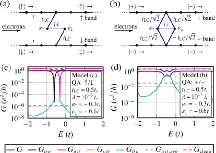
To explain the shape and order of magnitude ofGσ σ(E) of Fig.2, consider a toy model ˆH=Hˆ0+Hˆd+Vˆ that consists
FIG. 7. (Color online) (a) and (b) Tight-binding model to ratio- nalize the conductance curves of the AGNR with a single hydrogen adsorbate including two conducting bands, a localized state with spin
↑and↓, and a SOI between both localized states. The matrix elements between the quantum wire and the localized states are (a)tLCin the case of incoming electrons being spin polarized along↑/↓and (b) tLC/√
2 for+/− polarization. Here one hopping term is negative, see Eq. (B6). (c) and (d) Spin-dependent conductance for model parameters for the AGNR with hydrogen adatom and (c)↑/↓and (d)+/−quantization of incoming electrons. The SOI strengthλis estimated by the SOI strength of 2.5 meV for a hydrogen adatom on graphene [59] in relation to the graphene hoppingt=2.8 eV.
of the Hamiltonian of the lead and a single site Hˆ0= −t0
σ=↑,↓
x
( ˆc†x+1,σcˆx,σ+cˆ†x,σcˆx+1,σ), (B1) Hˆd=
σ=↑,↓
εσdˆσ†dˆσ+iλ( ˆd↑†dˆ↓−dˆ↓†dˆ↑), (B2)
and a coupling term
Vˆ =tLC
σ=↑,↓
( ˆdσ†cˆσ+cˆ†σdˆσ), (B3)
with ˆcσ≡cˆ0,σ. The whole model is sketched in Fig. 7(a).
It resembles a hydrogen adsorbate that splits off a resonant level [63,82–84] near the charge-neutral point from the conduction band continuum for both spin channels. The exchange interaction with the local spin lifts the degeneracy between the localized states with differing spin: ε↑=ε↓. In the case of a nonvanishing overlap matrix element tLC, the associated quasilocalized state contributes a separate conductance channel that interferes destructively with the residual ones [85]. The SOI is modeled to be only present at the resonant site by the parameterλ.
The model Eqs. (B1)–(B3) account for collinear conducting and local spins reflecting in the vanishing overlap between σ band and ¯σ quasilocalized state. The spin-dependent conductance of the collinear-spin model of Fig.7(a)is depicted in Fig.7(c). We observe the well-known conductance dips at the resonant energies ε↑ and ε↓ [63] and a small spin-flip conductance in the order of (λ/t)2 due to the small SOI parameterλ.
FIG. 8. (Color online) Average spin-flip conductance Gσσ ,avg¯ {arithmetic mean of Gσσ¯(E) and Gσ σ¯ (E) in the energy interval [−2t,2t]} for the model of Fig. 7 as function of the spacing =ε↑−ε↓ between the two localized levels with opposite spin.
The polarization in (a) is↑/↓[model Fig.7(a)] and in (b)+/− [model Fig.7(b)]. The SOI parameterλ and the hoppingtLC are chosen as in Figs.7(c)and7(d).
When rotating the spin quantization of incoming elec- trons by π/2 from↑/↓ to +/−, |+ =(|↑ + |↓)/√
2 and
|− =(|↑ − |↓)/√
2, an overlap of both quasilocalized states to both bands is formed. To account for this we generalize our model
Hˆ0 = −t0
μ=+,−
x
( ˆc†x+1,μcˆx,μ+cˆ†x,μcˆx+1,μ), (B4) Hˆd =
σ=↑,↓
εσdˆσ†dˆσ+iλ( ˆd↑†dˆ↓−dˆ↓†dˆ↑), (B5) and the coupling
Vˆ = tLC
√2[ ˆd↑†( ˆc++cˆ−)+dˆ↓†( ˆc+−cˆ−)+H.c.], (B6) where ˆc+=( ˆc↑+cˆ↓)/√
2 and ˆc−=( ˆc↑−cˆ↓)/√
2 [model in Fig.7(b)]. It now imitates the situation where the local moment and the conduction band spin are not collinear. Then, even in the absence of SOI, λ=0, the conduction band spin is not conserved and we expect a large spin-flip rate. Indeed, seen in Fig.7(d), the spin-flip conductance increases by four orders of magnitude compared to Fig. 7(c) even exceeding the spin-conserving conductance near the antiresonance. The
results of the model agree well with the conductance of the ribbon with a single hydrogen adatom in Fig.2: In particular, it also reproduces the quasilocalized state also seen in or near the band gap of the ribbon.
The results shown in Figs.7(c)and7(d)are qualitatively not strongly dependent on the level spacing=ε↑−ε↓, see Fig.8, as long asis larger than 0.05t for+/−polarization in Fig. 8(b). We mention that in the nonmagnetic case, ε↑=ε↓, the efficient spin-flip process for +/−polarization is suppressed, see Fig. 8(b) for →0. The reason is that in this case the single site effectively acts like a two-path interferometer that support perfect destructive interference for the two tunneling paths between the+and the−band.
APPENDIX C: COMPUTATION OF THE LOCAL CURRENT DENSITY
For completeness we summarize the calculation of the local current density responsej(r,E) starting from the full spin-dependent retarded Green’s function ˆG(E) [see Eq. (1) for its spin components]. The retarded Green’s function allows to calculate the nonequilibrium Keldysh Green’s function Gˆ<(E):
Gˆ<=iG[fˆ LˆL+fRˆR] ˆG†, (C1) with ˆα=i[ ˆα−( ˆα)†]. The occupation numbersfαof the leads reduce to step functions at zero (or low) temperature.
Inside the voltage window we assume an occupied left lead and an empty right lead, i.e., fL=1, fR=0, so that ˆG<
reduces to
Gˆ<(E)=iG(E) ˆˆ L(E) ˆG†(E). (C2) The Keldysh Green’s function is transformed to real-space representation using the basis functions of the underlying DFT calculation:G<σ σ(r,r,E)= rσ|Gˆ<(E)|rσ. The cur- rent density (per energy) is then expressed as
j(r,E)= 1 2π
2m
σ
rlim→r(∇r−∇r)G<σ σ(r,r,E). (C3) The factor 2π reflects an inverse Fourier transform.
[1] K. S. Novoselov, A. K. Geim, S. V. Morozov, D. Jiang, Y. Zhang, S. V. Dubonos, I. V. Grigorieva, and A. A. Firsov,Science306, 666(2004).
[2] W. Han, R. K. Kawakami, M. Gmitra, and J. Fabian, Nat.
Nanotechnol.9,794(2014).
[3] M. Gmitra, S. Konschuh, C. Ertler, C. Ambrosch-Draxl, and J. Fabian,Phys. Rev. B80,235431(2009).
[4] S. Roche and S. O. Valenzuela,J. Phys. D: Appl. Phys. 47, 094011(2014).
[5] M. B. Lundeberg, R. Yang, J. Renard, and J. A. Folk,Phys. Rev.
Lett.110,156601(2013).
[6] O. V. Yazyev and L. Helm,Phys. Rev. B75,125408(2007).
[7] D. Kochan, M. Gmitra, and J. Fabian,Phys. Rev. Lett. 112, 116602(2014).
[8] D. Kochan, S. Irmer, M. Gmitra, and J. Fabian, arXiv:1504.03898.
[9] M. Walz, J. Wilhelm, and F. Evers,Phys. Rev. Lett.113,136602 (2014).
[10] M. Droth and G. Burkard,Phys. Rev. B87,205432(2013).
[11] M. Droth and G. Burkard,Phys. Rev. B84,155404(2011).
[12] Y. W. Son, M. L. Cohen, and S. G. Louie,Phys. Rev. Lett.97, 216803(2006).
[13] A. Dasgupta, S. Bera, F. Evers, and M. J. van Setten,Phys. Rev.
B85,125433(2012).
[14] M. Fujita, K. Wakabayashi, K. Nakada, and K. Kusakabe, J. Phys. Soc. Jpn.65,1920(1996).
[15] K. Nakada, M. Fujita, G. Dresselhaus, and M. S. Dresselhaus, Phys. Rev. B54,17954(1996).
[16] L. Yang, M. L. Cohen, and S. G. Louie,Phys. Rev. Lett.101, 186401(2008).
[17] L. Talirz, H. S¨ode, J. Cai, P. Ruffieux, S. Blankenburg, R. Jafaar, R. Berger, X. Feng, K. M¨ullen, D. Passerone, R. Fasel, and C. A. Pignedoli,J. Am. Chem. Soc.135,2060(2013).
[18] G.-P. Guo, Z.-R. Lin, T. Tu, G. Cao, X.-P. Li, and G.-C. Guo, New J. Phys.11,123005(2009).
[19] M. Di Ventra, Electrical Transport in Nanoscale Systems (Cambridge University Press, Cambridge, 2008).
[20] N. M. R. Peres, A. H. Castro Neto, and F. Guinea,Phys. Rev. B 73,195411(2006).
[21] K. Wakabayashi,Phys. Rev. B64,125428(2001).
[22] A. Onipko,Phys. Rev. B78,245412(2008).
[23] M. Yamamoto, Y. Takane, and K. Wakabayashi,Phys. Rev. B 79,125421(2009).
[24] S. Ihnatsenka, I. V. Zozoulenko, and G. Kirczenow,Phys. Rev.
B80,155415(2009).
[25] A. La Magna, I. Deretzis, G. Forte, and R. Pucci,Phys. Rev. B 80,195413(2009).
[26] G. Cantele, Y.-S. Lee, D. Ninno, and N. Marzari,Nano Lett.9, 3425(2009).
[27] D. Soriano, F. Mu˜noz-Rojas, J. Fern´andez-Rossier, and J. J.
Palacios,Phys. Rev. B81,165409(2010).
[28] G.-H. Ding and C. T. Chan,J. Phys.: Condens. Matter23,205304 (2011).
[29] T.-T. Wu, X.-F. Wang, Y. Jiang, and L. Zhou, J. Nanosci.
Nanotechnol.12,6467(2012).
[30] R. Farghadan and E. Saievar-Iranizad, J. Appl. Phys. 111, 014304(2012).
[31] J. Bundesmann, M.-H. Liu, I. Adagideli, and K. Richter,Phys.
Rev. B88,195406(2013).
[32] T. P. Pareek and P. Bruno,Phys. Rev. B65,241305(2002).
[33] Y. Avishai and Y. Tokura,Phys. Rev. Lett.87,197203(2001).
[34] F. Zhai and H. Q. Xu,Phys. Rev. Lett.94,246601(2005).
[35] U. Aeberhard, K. Wakabayashi, and M. Sigrist,Phys. Rev. B72, 075328(2005).
[36] A. F. Sadreev and E. Y. Sherman, Phys. Rev. B 88, 115302 (2013).
[37] S. Bhattacharya, A. Akande, and S. Sanvito,Chem. Commun.
50,6626(2014).
[38] M. Modarresi, B. Kandemir, M. Roknabadi, and N.
Shahtahmasebi,J. Magn. Magn. Mater.367,81(2014).
[39] G. S. Diniz, M. R. Guassi, and F. Qu,J. Appl. Phys.116,113705 (2014).
[40] N. A. Mortensen and J. C. Egues,Phys. Rev. B 66, 153306 (2002).
[41] D. Peng, N. Middendorf, F. Weigend, and M. Reiher,J. Chem.
Phys.138,184105(2013).
[42] A. D. Becke,Phys. Rev. A38,3098(1988).
[43] A. Arnold, F. Weigend, and F. Evers,J. Chem. Phys.126,174101 (2007).
[44] J. Wilhelm, M. Walz, M. Stendel, A. Bagrets, and F. Evers,Phys.
Chem. Chem. Phys.15,6684(2013).
[45] A. Bagrets,J. Chem. Theory Comput.9,2801(2013).
[46] P. Schn¨abele, R. Koryt´ar, A. Bagrets, T. Roman, T. Schimmel, A. Groß, and F. Evers,J. Phys. Chem. C118,28252(2014).
[47] M. Walz, A. Bagrets, and F. Evers (unpublished).
[48] Methodological details: TURBOMOLE package [86], DFT with generalized gradient approximation (GGA [42], BP86 functional [87]), together with a contracted Gaussian-type basis
(def2-SVP) [80] and corresponding Coulomb-fitting basis set within the resolution of the identity (RI) approximation [88] in a two-component formalism [89,90].
[49] F. Evers and A. Arnold, in CFN Lectures on Functional Nanostructures - Volume 2, Lecture Notes in Physics, Vol. 820 (Springer, Berlin, 2011).
[50] J. Rioux and G. Burkard,Phys. Rev. B90,035210(2014).
[51] R. Landauer,IBM J. Res. Dev.1,223(1957).
[52] M. B¨uttiker, Y. Imry, R. Landauer, and S. Pinhas,Phys. Rev. B 31,6207(1985).
[53] D. S. Fisher and P. A. Lee,Phys. Rev. B23,6851(1981).
[54] B. J. van Wees, H. van Houten, C. W. J. Beenakker, J. G.
Williamson, L. P. Kouwenhoven, D. van der Marel, and C. T.
Foxon,Phys. Rev. Lett.60,848(1988).
[55] When changing the horizontal length of the device region with SOI, we observe an unchanged spin-flip conductance. We conclude that the spin-flip scattering occurs at the lead-device crossover probably caused by exchange with the magnetic zigzag edge states of the finite-size DFT calculation leaking into the device region, see Sec. III B and Appendix A 2 for a detailed discussion. This conceptual issue also reflects in the linear (and not quadratic) scaling of Gσσ¯ with the DOS, Gσσ¯(E)∼ρ(E), in the energy interval [−1.5 eV,1.5 eV]. How- ever, we can restrict the methodogical error ofGσσ¯ due to spin- flip scattering at the lead-device crossover by an upper bound of 10−10e2/ hwhich is orders of magnitude below the spin-flip conductance of hydrogenated AGNRs. Additionally, the spin- flip conductance of the clean AGNR11 due to SOI is bounded by 10−10e2/ h.
[56] H. Santos, M. C. Mu˜noz, M. P. L´opez-Sancho, and L. Chico, Phys. Rev. B87,235402(2013).
[57] A. H. Castro Neto and F. Guinea,Phys. Rev. Lett.103,026804 (2009).
[58] M. Gmitra, D. Kochan, and J. Fabian, Phys. Rev. Lett. 110, 246602(2013).
[59] J. Balakrishnan, G. K. W. Koon, M. Jaiswal, A. H. Castro Neto and B. ¨Ozyilmaz,Nat. Phys.9,284(2013).
[60] S. Irmer, T. Frank, S. Putz, M. Gmitra, D. Kochan, and J. Fabian, Phys. Rev. B91,115141(2015).
[61] In a non-SOI DFT calculation, there is no spatial information about the magnetization axis. In contrast, we get a spatial direction of the magnetization in a SOI DFT calculation. The reason for the magnetization axis being so close to thezaxis is the following: The extended H¨uckel guess as starting point for the SOI-DFT calculation computes one unpaired electron with spin polarization axis in defaultzdirection. This magnetization axis was already a local minimum and the self-consistent-field iteration of SOI DFT does not deviate much from this starting axis [91].
[62] In this work we do not discuss Kondo physics focusing on temperatures well above the Kondo scale TK. Indeed, there appears to be experimental evidence for a relatively small Kondo temperature in hydrogenated graphene, TK2 K [92]. For a recent review on Kondo impurities in graphene, we refer to Ref.
[93].
[63] T. C. Li and S. P. Lu,Phys. Rev. B77,085408(2008).
[64] B. Biel, X. Blase, F. Triozon, and S. Roche,Phys. Rev. Lett.
102,096803(2009).
[65] A. Lopez-Bezanilla, F. Triozon, and S. Roche,Nano Lett. 9, 2537(2009).
[66] A. Cresti, A. Lopez-Bezanilla, P. Ordej´on, and S. Roche,ACS Nano5,9271(2011).
[67] I. Deretzis, G. Fiori, G. Iannaccone, and A. La Magna,Phys.
Rev. B81,085427(2010).
[68] S. M.-M. Dubois, A. Lopez-Bezanilla, A. Cresti, F. Triozon, B. Biel, J.-C. Charlier, and S. Roche, ACS Nano 4, 1971 (2010).
[69] S. Ihnatsenka and G. Kirczenow, Phys. Rev. B 83, 245442 (2011).
[70] A. Lopez-Bezanilla and S. Roche, Phys. Rev. B86, 165420 (2012).
[71] C.-H. Chiu and C.-S. Chu,Phys. Rev. B85,155444(2012).
[72] K. Saloriutta, A. Uppstu, A. Harju, and M. J. Puska,Phys. Rev.
B86,235417(2012).
[73] T. Lehmann, D. A. Ryndyk, and G. Cuniberti,Phys. Rev. B88, 125420(2013).
[74] S. Ihnatsenka and G. Kirczenow, Phys. Rev. B 88, 125430 (2013).
[75] J. Wilhelm, M. Walz, and F. Evers,Phys. Rev. B89,195406 (2014).
[76] C. H. Chiu and C. S. Chu,Phys. Rev. B90,195436(2014).
[77] M. D. Petrovi´c and F. M. Peeters,Phys. Rev. B 91, 035444 (2015).
[78] K. M. McCreary, A. G. Swartz, W. Han, J. Fabian, and R. K.
Kawakami,Phys. Rev. Lett.109,186604(2012).
[79] Apart from a factor of 2 in the matrix sizes, the main computa- tional cost for the full spin treatment is a slow convergence in the self-consistent field (SCF) cycle of the DFT. This is due to many possible spin configurations with (nearly) equal energy.
Physically this is the same effect as in a spin glass [94]: flipping a single spin is energetically hardly suppressed if neighboring
spins are also flipped. The larger the system gets, the more low lying spin excitation exist in a given energy window; making the SCF convergence extremely costly for larger systems.
[80] A. Sch¨afer, H. Horn, and R. Ahlrichs,J. Chem. Phys.97,2571 (1992).
[81] P.-O. L¨owdin,J. Chem. Phys.18,365(1950).
[82] A. H. Castro Neto, F. Guinea, N. M. R. Peres, K. S. Novoselov, and A. K. Geim,Rev. Mod. Phys.81,109(2009).
[83] V. M. Pereira, F. Guinea, J. M. B. Lopes dos Santos, N. M.
R. Peres, and A. H. Castro Neto,Phys. Rev. Lett.96,036801 (2006).
[84] V. H¨afner, J. Schindler, N. Weik, T. Mayer, S. Balakrishnan, R.
Narayanan, S. Bera, and F. Evers,Phys. Rev. Lett.113,186802 (2014).
[85] P. A. Orellana, F. Dom´ınguez-Adame, I. G´omez, and M. L.
Ladr´on de Guevara,Phys. Rev. B67,085321(2003).
[86] R. Ahlrichs, M. B¨ar, M. H¨aser, and C. K¨olmel,Chem. Phys.
Lett.162,165(1989).
[87] J. P. Perdew,Phys. Rev. B33,8822(1986).
[88] K. Eichkorn, F. Weigend, O. Treutler, and R. Ahlrichs,Theor.
Chem. Acc.97,119(1997).
[89] M. K. Armbruster, F. Weigend, C. van W¨ullen, and W. Klopper, Phys. Chem. Chem. Phys.10,1748(2008).
[90] A. Baldes and F. Weigend,Mol. Phys.111,2617(2013).
[91] I. Beljakov, V. Meded, F. Symalla, K. Fink, S. Shallcross, M. Ruben, and W. Wenzel,Nano Lett.14,3364(2014).
[92] R. R. Nair, M. Sepioni, I. Tsai, O. Lehtinen, J. Keinonen, A. V.
Krasheninnikov, T. Thomson, A. K. Geim, and I. V. Grigorieva, Nat. Phys.8,199(2012).
[93] L. Fritz and M. Vojta,Rep. Prog. Phys.76,032501(2013).
[94] K. Binder and A. P. Young,Rev. Mod. Phys.58,801(1986).
![FIG. 8. (Color online) Average spin-flip conductance G σ σ ,avg ¯ {arithmetic mean of G σ σ¯ (E) and G σ σ¯ (E) in the energy interval [ − 2t,2t] } for the model of Fig](https://thumb-eu.123doks.com/thumbv2/1library_info/5588994.1690674/7.911.78.443.106.257/color-online-average-conductance-arithmetic-energy-interval-model.webp)
