Absence of a giant spin Hall effect in plasma-hydrogenated graphene
Tobias Völkl,1Denis Kochan,2Thomas Ebnet,1Sebastian Ringer,1Daniel Schiermeier,1Philipp Nagler,1Tobias Korn,1,*
Christian Schüller,1Jaroslav Fabian,2Dieter Weiss,1and Jonathan Eroms1,†
1Institut für Experimentelle und Angewandte Physik, Universität Regensburg, 93053 Regensburg, Germany
2Institut für Theoretische Physik, Universität Regensburg, 93053 Regensburg, Germany
(Received 27 September 2018; published 1 February 2019)
The weak spin-orbit interaction in graphene was predicted to be increased, e.g., by hydrogenation. This should result in a sizable spin Hall effect (SHE). We employ two different methods to examine the spin Hall effect in weakly hydrogenated graphene. For hydrogenation we expose graphene to a hydrogen plasma and use Raman spectroscopy to characterize this method. We then investigate the SHE of hydrogenated graphene in the H-bar method and by direct measurements of the inverse SHE. Although a large nonlocal resistance can be observed in the H-bar structure, comparison with the results of the other method indicate that this nonlocal resistance has a non-spin-related origin.
DOI:10.1103/PhysRevB.99.085401
I. INTRODUCTION
Covalently bonded hydrogen was predicted to significantly increase the spin-orbit coupling (SOC) of graphene by Castro Neto and Guinea [1]. However, experimental results on this were conflicting. Balakrishnanet al.reported a high nonlocal resistance in weakly hydrogenated graphene in the so-called H-bar structure [2]. They further observed an oscillatory behavior of this nonlocal resistance with an in-plane magnetic field and therefore attributed this effect to the SHE with a spin Hall angle of aroundαSH =0.18–0.45. A high nonlocal resistance in similar samples was also observed by Kaverzin and van Wees [3]. However, they obtained an unrealistically high value for the spin Hall angle of αSH =1.5 and could not observe any effect of an in-plane magnetic field on this nonlocal resistance. They therefore argue that this nonlocal signal has a non-spin-related origin.
Here, we perform different types of experiments to solve this controversy. For hydrogenation we expose graphene to a hydrogen plasma which has several advantages over the hydrogenation method by exposing hydrogen silsesquioxane (HSQ) to an electron beam, as employed in Refs. [2,3]. We use Raman spectroscopy to characterize graphene exposed to hydrogen or deuterium to verify that the defects created by this method are indeed bonded hydrogen atoms. Then we perform nonlocal measurements in the so-called H-bar geometry in graphene that was hydrogenated by this method.
Further, we employ electrical spin injection into hydrogenated graphene to perform spin transport measurements as well as measurements of the inverse spin Hall effect. Our results show that the large nonlocal signal in hydrogenated graphene is not related to the spin Hall effect.
*Present address: Institut für Physik, Universität Rostock, 18059 Rostock, Germany.
†jonathan.eroms@ur.de
II. PLASMA HYDROGENATION OF GRAPHENE Due to limitations of the HSQ-based hydrogenation pro- cedure, which we describe in more detail below, we explore hydrogenation by exposing graphene to a hydrogen plasma in a reactive ion etching chamber. Following the recipe de- veloped by Wojtaszek et al. [4], exfoliated graphene was exposed to hydrogen plasma with pressure p=40 mTorr, 30-sccm gas flow, and 2 W of power. The relatively low power leads to a low acceleration bias voltage ofUbias<2 V, which reduces the creation of lattice defects. The samples were then investigated using Raman spectroscopy.
Figure 1(a) shows the Raman spectra of samples with different plasma exposure times. With increasing exposure time both a Dpeak and aD peak arise, which indicate the presence of defects. For higher exposure times a decrease of the 2D-peak intensity can be observed, which indicates an alteration of the electronic band structure. As can be seen from the red curve in Fig. 1(c), the ratio between the D- andG-peak intensities increases with exposure time up to a value aroundID/IG=3 for an exposure time oft =40 s and decreases for longer exposure times. For low defect densities the ratio betweenD- andG-peak intensities is proportional to the defect density [5]:
nD(cm−2)=1.8±0.5× 10²² λ4L
ID
IG
, (1)
with λL=532 nm [given in nanometers in Eq. (1)] being the excitation wavelength.ID/IGreaches its maximum when the average distance between defects becomes comparable to the distance an electron-hole pair travels in its lifetime, given by lx=vF/ωD, with ωD being the D-peak frequency [5]. At higher defect densities theDpeak becomes broader, and its intensity decreases. Further, at high defect densities the graphene band structure is altered by the defects, which reduces possible transitions [6]. Since the 2Dpeak is doubly resonant, it is more sensitive to this alteration than the D and G peaks, and therefore, a reduction of the 2D-peak
1200 1400 1600 2600 2800
Hydrogen 10s 20s
40s 60s 180s
I(arb.units)
Raman shift(cm-1) (a)D
GD' 2D
1200 1600 2000 2400 2800
D
Deuterium 10s 20s
40s 60s 120s
I(arb.units)
Raman shift(cm-1) (b)
GD' 2D
0 30 60 90 120 150 180
0.0 0.5 1.0 1.5 2.0 2.5 3.0
I D/I G
t(s)
pre annealing mean pre annealing post annealing mean post annealing (c)
50 100 150 200 250 300
0.0 0.2 0.4 0.6 0.8 1.0
I
D/I
Gafter a nnealing
T(°C)
Hydrogen Deuterium
(d)
FIG. 1. (a) Raman spectra for different exposure times with hydrogen plasma. An increase ofD- andD-peak intensities as well as a decrease of the 2D-peak intensity with increasing plasma exposure time can be observed, indicating the creation of defects. (b) Raman spectra for different exposure times with deuterium plasma. The deuterium seems to create more defects than hydrogen for the same exposure times.
(c) Ratio betweenD- andG-peak intensities with hydrogen plasma exposure time before (red curve) and after (green curve) annealing atT = 320◦C.ID/IGincreases up to an exposure time oft=40 s and decreases for high exposure times. For low exposure times the hydrogenation process is reversible. (d)ID/IGafter annealing at different temperatures normalized to its initial value for hydrogen (black dots) and deuterium (red dots) with a plasma time oft=20 s. Deuterium is stabler with increasing temperature than hydrogen. This is a strong indication that the defects created by this method are bonded hydrogen (deuterium) atoms.
intensity with increasing exposure time can be observed in Fig.1(a).
The green curve in Fig. 1(c) shows ID/IG for the same samples after annealing in vacuum at 320◦C for 1 h. For low plasma exposure timest 40 s annealing almost fully removes the defects. Since this temperature is too low to heal vacancies [7] in graphene, this behavior indicates that for these low exposure times the observed defects are bonded hy- drogen atoms. Fort >40 s the defects could not be removed by annealing. Therefore, the occurrence of lattice defects for higher plasma exposure times is likely. Possible explanations for this might be heating of the samples during the exposure process or etching of carbon atoms by the formation of CH2 after saturation of the hydrogen coverage of graphene [8].
To further determine the type of observed defects the same experiment was performed with deuterium instead of hydrogen. Figure 1(b) shows Raman spectra for different exposure times. In comparison to Fig.1(a)deuterium seems to induce slightly more defects than hydrogen, as can be seen by the rapid decrease of the 2D-peak intensity in Fig.1(b). One explanation for this could be higher reactivity of deuterium due to a slightly increased binding energy [9]. Another expla- nation is that the deuterium atoms are more likely to create lattice defects due to their higher mass.
Samples exposed to either hydrogen or deuterium with an exposure time oft =20 s were annealed for 1 h in vacuum at different temperatures. Figure1(d)shows the relativeID/IG
ratio divided by its value before annealing. Surprisingly, the bonded deuterium [red dots in Fig.1(d)] is more stable with temperature than the hydrogen [black dots in Fig. 1(d)]. A similar behavior has been observed for hydrogen and deu- terium on graphite [10]. This can be explained by a slightly increased binding energy of deuterium due to zero-point energy effects [9] and a lower attempt frequency due to the higher mass of deuterium compared to hydrogen, hindering desorption [10]. The fact that a different desorption behavior was found for hydrogen and deuterium is a clear indication that the defects created by this method are really bonded hydrogen since there should be no difference for other defect types.
Concerning the HSQ-based hydrogenation method em- ployed in Refs. [2,3,11], we note several difficulties. First, the HSQ film cannot be removed after exposure without destroy- ing the underlying graphene sheet. Therefore, hydrogenation can be done only as a last step of the sample fabrication. Since resist residues from previous steps proved to prevent efficient hydrogenation, it is expected that the hydrogen coverage produced by this method is not homogeneous. Second, a high
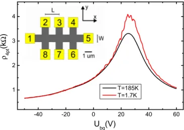
-40 -20 0 20 40 60 1
2 3 4
ρ 4pt(kΩ)
Ubg(V)
T=185K T=1.7K
FIG. 2. Back-gate-dependent four-point resistivity of the H-bar sample at T =185 K (black curve) and T =1.7 K (red curve).
This gives a position of the charge neutrality point atUCNP=26 V, indicatingp-type doping and a mobility aroundμ=1600 cm2/V s.
Inset: Schematic picture of an H-bar sample.
p-type doping was always observed in samples produced with this method both in our measurements [12] and in the mea- surements by Kaverzin and van Wees [3]. This is problematic since the occurrence of the SHE is expected only close to the charge neutrality point (CNP) [13], which in these samples is often not accessible due to the high doping. Third, it is not entirely clear that the defects produced by this method are really bonded hydrogen since the Raman measurements are not sensitive to the defect type. Therefore, in our experiments, we resort to plasma hydrogenation.
III. NONLOCAL RESISTANCE IN HYDROGENATED GRAPHENE
Using plasma hydrogenation, a Hall-bar sample was fab- ricated. First, exfoliated graphene was exposed to hydrogen plasma for 20 s, as described in the previous section. After- wards, oxygen plasma was used to etch the graphene into a Hall bar, and 0.5 nm of Cr and 60 nm of Au were deposited for contacts. A schematic picture of the sample structure is displayed in the inset of Fig. 2. Raman measurements of this sample revealID/IG=0.43. Using Eq. (1) and assuming that the defect density equals the hydrogen atom density, we extract a coverage of 0.0025%. This value is much lower than in the previous section for the same exposure time because several lithography steps, and therefore, resist bakeout steps were necessary after the hydrogenation process. However, employing hydrogenation as a first step in the sample fabri- cation process was preferred over using it as a last step since it is expected that resist residues lead to an inhomogeneous hydrogen coverage of the sample.
Back gate sweeps of the four-point resistivity of this sample at temperatures T =185 K (black curve) and T = 1.7 K (red curve) are depicted in Fig. 2. In this sample p-type doping with UCNP=26 V and mobilities of μh = 1400 cm2/V s (μh=1500 cm2/V s) for the hole side and μel=1800 cm2/V s (μel=2000 cm2/V s) for the electron side atT =185 K (T =1.7 K) were observed.
To obtain the nonlocal resistance, a current was applied between contacts 2 and 8 in the inset of Fig.2, and voltage was measured between contacts 3 and 7 [Fig.3(a)] and between contacts 4 and 6 [Fig. 3(b)]. Decreasing the temperature from T =185 K [black curves in Figs. 3(a) and 3(b)] to T =1.7 K [green curves in Figs. 3(a) and 3(b)] increases the nonlocal resistance close to the charge neutrality point.
The red curves depict the expected Ohmic contribution given byROhmic =R2ptG, withR2pt being the two-point resistance between contacts 2 and 8 and a geometry factorGdetermined by a finite-element simulation done withCOMSOL. As can be seen in Figs.3(a)and3(b), close to the charge neutrality point the measured nonlocal resistances far exceed the expected Ohmic contribution.
As argued by Balakrishnanet al. [2], this nonlocal resis- tance might be caused by an interplay between direct and inverse spin Hall effects. Then the nonlocal resistance as a function of distance to the current pathLis given by [14]
Rnl = 1 2α2SHρW
λs
exp
−L λs
, (2)
withρbeing the sheet resistivity,W being the sample width, andλs being the spin diffusion length. By comparingRnl at the two different distances in Figs.3(a) and3(b) λs can be calculated to be in the range ofλs=510–565 nm. With this the spin Hall angleαSHclose to the charge neutrality point can be calculated to beαSH =1.3 forT =185 K andαSH =1.6 forT =1.7 K. These unrealistically high values are similar to the one reported by Kaverzin and van Wees [3].
Further, in the case where the large nonlocal resistance is caused by the spin Hall effect,Rnl should be sensitive to an in-plane magnetic field due to Larmor precession of the spins.
Therefore, an oscillatory behavior ofRnlis expected to follow [14]:
Rnl(B||)= 1
2α2SHρWRe{(
1+iωLτs/λs)
×exp[−(
1+iωLτs/λs)L],}
(3)
withωLbeing the Larmor frequency.
Figures3(c)and3(d)show the influence of magnetic field in both in-plane directions (black and red curves) onRnl for two different distances from the current path. As can be seen, no significant change inRnl withB||can be observed. This is in disagreement with the expected behavior given by Eq. (3), which is depicted in Figs.3(e)and3(f)for different values of τsin a realistic range since a lower bound ofτs>10 ps could be established due to the absence of a weak antilocalization peak [12]. As indicated here, a significant dependence ofRnl
onB||should be visible.
IV. INVERSE SPIN HALL EFFECT IN HYDROGENATED GRAPHENE
Due to the difficulties arising from measuring the spin Hall effect in the H-bar geometry a more direct way to observe this effect is desirable. One way to examine the inverse spin Hall effect electrically was explored by Valenzuela and Tinkham [15] with aluminum wires. For this they employed electrical
-40 -20 0 20 40 60 0
40 80 120 160
Rnl(2μm)(Ω)
Ubg(V)
T=1.7K T=185K Rohmic (a)
-1.0 -0.5 0.0 0.5 1.0
115 116 117
Bx By
Rnl(2μm)(Ω)
B(T) (c)
-1.0 -0.5 0.0 0.5 1.0
-50 0 50 100 150
τs=10 ps τs=20 ps τs=100 ps
Rnl(2μm)(Ω)
B||(T) (e)
-60 -40 -20 0 20 40 60
0 2 4 6
Rnl(4μm)(Ω)
Ubg(V)
T=1.7K T=185K Rohmic (b)
-1.0 -0.5 0.0 0.5 1.0
3.0 3.1
Rnl(4μm)(Ω)
B(T)
Bx By (d)
-1.0 -0.5 0.0 0.5 1.0
-2 -1 0 1 2 3
4 τ
s=10 ps τs=20 ps τs=100 ps
Rnl(4μm)(Ω)
B||(T) (f)
FIG. 3. (a) and (b) Charge carrier density dependence of nonlocal resistance measured at two different distances to the current path at T =185 K (black curves) andT =1.7 K (green curves). In both cases the nonlocal resistance exceeds the expected Ohmic contribution (red curves) close to the charge neutrality point. (c) and (d) Dependence ofRnlon a magnetic field in both in-plane directions (black and red curves).
No noticeable influence ofB||onRnlcan be observed. (e) and (f) Simulation of the in-plane magnetic field dependence ofRnl expected from the spin Hall effect with different spin lifetimes and for different distances from the current path.
spin injection to create a spin current through the wire and measured the resulting nonlocal voltage across a Hall bar.
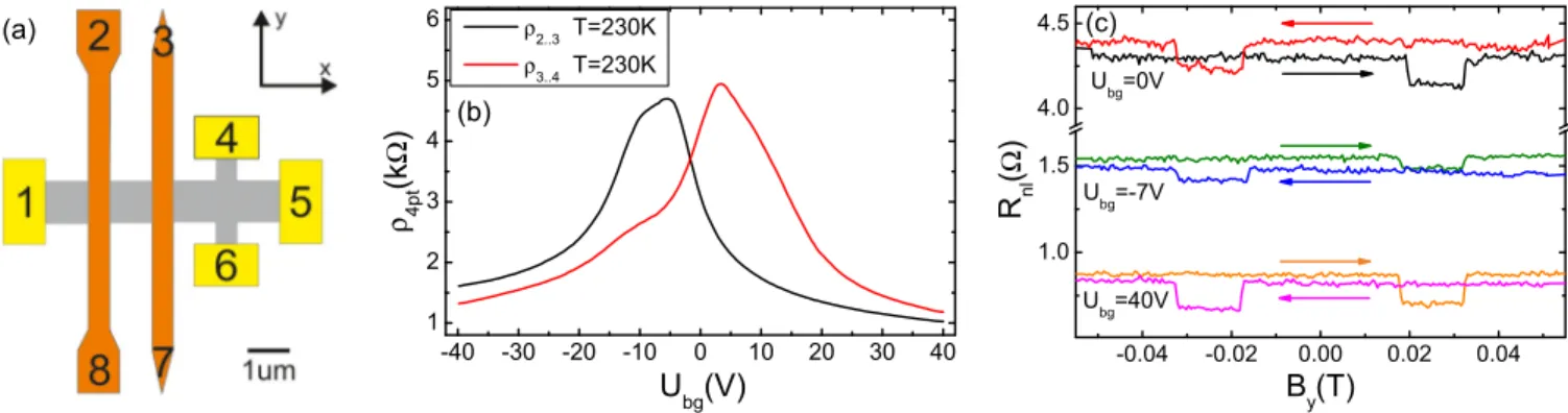
To employ this method in hydrogenated graphene the sample shown schematically in Fig.4(a)was fabricated. First, exfoliated graphene was exposed to hydrogen plasma for 20 s.
Spin injection contacts consisting of 1.2 nm of MgO, acting as a tunnel barrier; 50 nm of Co; and 10 nm of Au were deposited [orange stripes in Fig.4(a)]. Afterwards, 0.5 nm of Cr and 80 nm of Au were deposited for contacts. In the last step oxygen plasma was employed to etch the sample.
Figure4(b)shows back gate sweeps of this sample, where a current was applied between contacts 1 and 5 and the voltage was taken between contacts 2 and 3 [black curve in Fig.4(b)]
and between contacts 3 and 4 [red curve in Fig.4(b)]. As can be seen, the position of the charge neutrality point differs for the two areas. This can be caused by different dopings of the areas either by the ferromagnetic contacts or by a difference in hydrogen coverage between the area underneath the stripes and the rest of the sample. Mobilities ofμh =2000 cm2/V s for the hole side andμel =2400 cm2/V s for the electron side could be observed in this sample.
Further, nonlocal spin injection measurements were per- formed to examine whether spin injection is possible with these contacts [16]. Figure 4(c) shows nonlocal spin-valve measurements at different back gate voltages. Here, a current is applied between contacts 3 and 5 in Fig. 4(a), and a nonlocal voltage is measured between contacts 2 and 1. The magnetization of the ferromagnetic stripes is first aligned by a magnetic field in the stripe direction of By=1 T. Then the magnetic field is swept in the opposite direction. Due to their different shapes the two ferromagnet stripes have different coercive fields. As can be seen in Fig.4(c), a clear
difference between parallel and antiparallel alignments of the stripe magnetizations can be observed over the whole back gate range.
Applying an out-of-plane magnetic field to this setup leads to precession of the spins around that field. The out-of-plane magnetic field dependence is depicted in Fig. 5. Here, a parabolic background that can be caused by the charge current contribution in the nonlocal path due to the presence of pinholes in the tunnel barriers [17] was subtracted. In the low-magnetic-field range the nonlocal resistance follows the expected behavior of the Hanle-effect [18]:
Rnl(ωL)=Rnl(0) ∞
0
√ 1
4πDst exp
− L2 4Dst
×cos(ωLt) exp
−t τs
dt, (4)
Rnl(0)= P2ρλs
2W exp(−L/λs).
Fitting the data in the low-magnetic-field range (red curve in Fig.5) reveals a spin injection efficiency ofP=3.1%. The injection efficiency is much lower than what is typically ob- served with these kinds of tunnel barriers in pristine graphene.
This can be caused by enhanced island growth of the MgO tunnel barrier due to the attached hydrogen and therefore an increase in pinholes in the barrier, resulting in a relatively low contact resistance of Rc=1.2–4.2 k μm2. Another explanation might be increased spin relaxation in the barrier due to the hydrogen atoms. It has to be noted that fabricating spin-selective contacts in graphene that was hydrogenated using this method proved to be difficult in general.
-40 -30 -20 -10 0 10 20 30 40 1
2 3 4 5 6
ρ 4pt(kΩ)
Ubg(V)
ρ2..3 T=230K ρ3..4 T=230K (b)
-0.04 -0.02 0.00 0.02 0.04 1.0
1.5 4.0 4.5
Ubg=40V Ubg=-7V
R nl(Ω)
By(T) (c)
Ubg=0V
(a)
FIG. 4. (a) Schematic picture of a sample for measuring the inverse spin Hall effect. (b) Back gate sweeps of the inverse spin Hall effect sample. Two areas of the sample (black and red curves) show different dopings. (c) Nonlocal spin-valve measurements at different back gate voltages. The reversal of the magnetization of the injection contacts is clearly visible in the nonlocal resistance.
Further, the extracted spin lifetime ofτs=146 ps is much smaller than what was observed in pristine graphene with tunneling contacts produced by the same method [19]. This is in contrast to the findings of Wojtaszeket al., who observed an increase in spin lifetime after treating pristine graphene with hydrogen plasma [20]. This small value for the spin lifetime can be caused by either an increased contact-induced spin relaxation due to an increase in the number of pinholes [21] or increased spin relaxation caused by the presence of hydrogen atoms acting as magnetic impurities [22]. However, τsis still large enough that a clear oscillation of the nonlocal resistance in the H-bar geometry should be visible, as shown by Figs.3(e)and3(f).
At higher magnetic fields the stripe magnetization rotates into the out-of-plane directions. Therefore, the polarization of the injected spins has an out-of-plane component that does not precess around the external field. The nonlocal resistance saturates around a magnetic field ofBz=1.8 T. This value coincides with the field at which the magnetization direction is completely rotated into the out-of-plane direction, determined by anisotropic magnetoresistance measurements [12].
Contrary to similar measurements performed by Tombros et al. in pristine graphene [23], no difference between the
-3 -2 -1 0 1 2 3
-0.05 0.00 0.05 0.10 0.15 0.20
P=3.1 % τs=146 ps λs=0.93 μm
Δ
R
nl(
Ω)
B
z(T)
FIG. 5. Nonlocal resistance after subtraction of a parabolic back- ground (black curve) atUbg=0 V. The Hanle peak at low magnetic field can be fitted with Eq. (4) (red curve). At high magnetic field the stripe magnetization is rotated in the magnetic field direction.
zero-magnetic-field value and the saturation value of the nonlocal resistance could be observed. This indicates isotropic spin relaxation, consistent with the expected dominating spin relaxation mechanisms of contact-induced spin relaxation and spin relaxation due to spin-flip scattering at the absorbed hydrogen atoms. Both mechanisms result in isotropic spin relaxation.
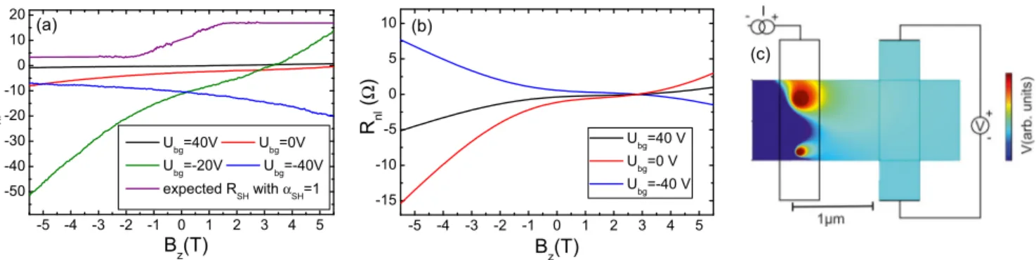
For measurement of the inverse spin Hall effect a current was applied between contacts 3 and 1 in Fig.4(a), and nonlo- cal voltage was measured between contacts 4 and 6. Without an external magnetic field the stripe magnetization is in the in-plane direction. Therefore, no nonlocal voltage due to an inverse spin Hall effect is expected. Applying an out-of-plane magnetic field results in a rotation of the stripe magnetization towards the out-of-plane direction. The resulting out-of-plane component of the spin polarization then leads to nonlocal voltage that is expected to follow [15]:
RSH =1
2PαSHρexp(−L/λs) sin(θ), (5) with sin(θ) being the projection of the stripe magnetization on thezaxis. With Eq. (4) saturation of the nonlocal resistance at Bz=1.8 T with RSH = αPSHλWs Rnl(0)≈αSH ×6.9is ex- pected. The expected resultingRSH withαSH =1 is depicted by the purple curve in Fig. 6(a). For this the angular de- pendence of the magnetization direction sin(θ) was extracted from Fig.5[15], and an offset was added for clarity.
The observed nonlocal resistance in this geometry for different back gate voltages is shown in Fig. 6(a). Here, a large magnetic-field-dependent nonlocal resistance can be seen. However, no saturation of this nonlocal resistance for Bz>1.8 T was observed. The magnetic field dependence of the nonlocal resistance is therefore unlikely to be caused by the spin Hall effect.
To determine the origin of this effect a finite-element simulation done with COMSOL was performed. For this the potential distribution in the presence of two pinholes in the tunnel barrier was calculated (similar to the calculations in Ref. [17]), as shown in Fig. 6(c). The resulting magnetic field dependence for different charge carrier concentrations shown in Fig.6(b) is comparable to the nonlocal resistance in Fig.6(a). Therefore, it is likely that the observed magnetic field dependence of the nonlocal resistance is caused by a charge current effect due to the presence of pinholes.
-5 -4 -3 -2 -1 0 1 2 3 4 5 -50
-40 -30 -20 -10 0 10 20
Ubg=40V Ubg=0V Ubg=-20V Ubg=-40V expected RSHwithαSH=1
Rnl(Ω)
Bz(T) (a)
-5 -4 -3 -2 -1 0 1 2 3 4 5 -15
-10 -5 0 5 10
R nl(Ω)
Bz(T)
Ubg=40 V Ubg=0 V Ubg=-40 V (b)
(c)
FIG. 6. (a) Nonlocal resistance in the inverse spin Hall effect geometry at different back gate voltages. No saturation of the nonlocal resistance can be observed. The purple curve depicts the expectedRSHgiven by Eq. (5) withαSH =1. (b) Magnetic-field-dependent nonlocal resistance for different charge carrier concentrations. (c) Potential distribution over the simulated sample in the presence of two pinholes.
This effect can mask a potential inverse spin Hall effect sig- nal. However, the large spin Hall angle ofαSH ≈1 resulting from the spin Hall interpretation of the H-bar geometry should still be observable close to the charge neutrality pointUCNP = 10 V of the areas that are not covered by the ferromagnetic stripes.
V. SPIN HALL ANGLE: AN ESTIMATION OF ORDER OF MAGNITUDE
In this section we provide a theoretical estimate of the upper bound of the spin Hall angle αSH that conventionally expresses a rate conversion of the charge to the transverse spin current in the presence of SOC. To model hydrogen chemisorption, we employ the tight-binding Hamiltonian in- spired by first-principles calculations proposed in Ref. [24].
Plain graphene is described by the conventional nearest- neighbor HamiltonianH0, and the hydrogen-induced pertur- bation including locally enhanced SOC is described by the HamiltonianH (see Refs. [24,25]). Related transport char- acteristics are estimated using the methodology developed in Refs. [13,26]. Particularly, for a given scattering process n,s→n˜,s, where an electron with the incident direction and˜ spinn,selastically scatters to an outgoing state ˜n,˜s, we calcu- late the corresponding differential cross section ddσϕ(n,s; ˜n,˜s) that also depends on the energy of the incident electron.
Knowing ddσϕ, we know the spatial probability distributions of electrons with flipped or conserved spin depending on the relative angle ˜ϕn=(nn˜). Elastic scattering governed byH affects momentum relaxation due to resonances near the Dirac point [27,28] and also spin relaxation due to locally enhanced SOC [26,29,30]. Despite the fact that hydrogen is predicted to induce also an unpaired magnetic moment [31], which can serve as another spin relaxation channel [22], we restrict our estimates ofαSH to the local SOC interactions.
Assuming a spin-polarized beam of, say, spin-up electrons with incident energyE, the upper bound of the spin Hall angle αSH(E) reads
αSH(E)≈ n˜ dσ
dϕ(n,↑; ˜n,↑)−ddσϕ(n,↓; ˜n,↑) sin ˜ϕn
˜ n
dσ
dϕ(n,↑; ˜n,↓) 2 cos ˜ϕn
,
(6)
where the angle brackets represent averaging over all in- coming directionsn. The calculation was performed for one hydrogen atom in a supercell containing 16 120 carbon atoms, i.e., a hydrogen concentration of 0.0062%. Figure7displays αSH as a function of Fermi energy. The obtained values are comparable in magnitude to, e.g., those of Ferreiraet al.[13]
but differ from the experimental data fitted by Eq. (2). Further, as seen in Fig. 7, αSH is expected to vanish at the charge neutrality point, which is in contrast to the observed nonlocal resistance in Fig. 3. We note that a more advanced Kubo- based approach to the spin conductivity in the presence of higher concentrations and cluster formations was investigated in Refs. [32–35].
VI. DISCUSSION
The background effect observed in Fig.6could mask the relatively small spin Hall angle resulting from the theoretical estimation in Fig. 7. However, the high value of αSH >1 following the SHE interpretation of the nonlocal resistance in Figs. 3(a) and 3(b) should still be observable. Further, this unusually high spin Hall angle and the absence of an
-0.4 -0.2 0.0 0.2 0.4
-0.004 -0.002 0.000 0.002 0.004
α SH
E(eV)
FIG. 7. Estimated spin Hall angleαSH at zero temperature for dilute hydrogenated graphene as a function of Fermi energy (zero energy corresponds to the charge neutrality point). The tight-binding parameters and model-based calculation follow [24,26].
oscillatory behavior of Rnl with an in-plane magnetic field support the findings of Kaverzin and van Wees [3]. These results suggest that the large nonlocal resistance observed in Figs.3(a)and3(b)is caused by a non-spin-related mechanism.
Large nonlocal resistances in the H-bar structure were also observed in graphene decorated with heavy atoms [36], hexagonal boron nitride/graphene heterostructures [37], and graphene structured with an antidot array [38]. They were attributed to the occurrence of a valley-Hall effect [36,37], nonzero Berry curvature due to the presence of a band gap [38], and transport through evanescent waves [34,39].
However, none of these effects can sufficiently explain the observed behavior [12]. Regarding the valley Hall effect in particular [30,40], we note that the short-range nature of scattering at the hydrogen resonance causes strong valley mixing and hence effectively washes out the valley Hall effect.
This is corroborated by the short intervalley time extracted from the weak localization measurement [12]. As a possible alternative mechanism, we speculate that increased disorder by the adsorbates leads to enhanced charge inhomogeneity.
Around the charge neutrality point, this will create randomly positioned p-n junctions, which can guide the electron path as in electron optics [41], causing a deviation from diffusive Drude transport.
VII. CONCLUSION
In conclusion we employed two different types of mea- surements to investigate the spin Hall effect in hydrogenated
graphene. For hydrogenation, graphene was placed into a hydrogen plasma. This technique was investigated by Raman spectroscopy. Since Raman measurements are sensitive to only the number of defects and not to the defect type, mea- surements with both hydrogen and deuterium were performed.
The different desorption behaviors observed for these isotopes are a clear indication that the defects produced by this method are indeed bonded hydrogen atoms.
Nonlocal measurements in the so-called H-bar geometry showed a large nonlocal resistance that, however, did not show a dependence on an in-plane magnetic field. Also measure- ment of the inverse spin Hall effect by electrical spin injection showed no sign of the large spin Hall angle suggested by the spin Hall effect interpretation of the nonlocal measurements.
Further, a theoretical estimate showed a much smaller spin Hall angle than suggested by the spin Hall interpretation of the nonlocal resistance in the H-bar method. These results indicate that the large nonlocal resistance has a non-spin- related origin.
ACKNOWLEDGMENTS
Financial support by the Deutsche Forschungsgemein- schaft (DFG) through Project KO 3612/3-1 and within the programs GRK 1570, SFB 689, and SFB 1277 (Projects A09, B05, and B06) is gratefully acknowledged. This project has received funding from the European Union’s Horizon 2020 research and innovation program under Grant Agreement No.
696656 (Graphene Flagship).
[1] A. H. Castro Neto and F. Guinea,Phys. Rev. Lett.103,026804 (2009).
[2] J. Balakrishnan, G. K. W. Koon, M. Jaiswal, A. H. Castro Neto, and B. Ozyilmaz,Nat. Phys.9,284(2013).
[3] A. A. Kaverzin and B. J. van Wees,Phys. Rev. B91,165412 (2015).
[4] M. Wojtaszek, N. Tombros, A. Caretta, P. H. M. van Loosdrecht, and B. J. van Wees,J. Appl. Phys.110,063715(2011).
[5] L. G. Cancado, A. Jorio, E. H. M. Ferreira, F. Stavale, C. A.
Achete, R. B. Capaz, M. V. O. Moutinho, A. Lombardo, T. S.
Kulmala, and A. C. Ferrari,Nano Lett.11,3190(2011).
[6] A. C. Ferrari,Solid State Commun.143,47(2007).
[7] E. Zion, A. Butenko, Y. Kaganovskii, V. Richter, L. Wolfson, A. Sharoni, E. Kogan, M. Kaveh, and I. Shlimak,J. Appl. Phys.
121,114301(2017).
[8] Z. Luo, T. Yu, K.-j. Kim, Z. Ni, Y. You, S. Lim, Z. Shen, S. Wang, and J. Lin,ACS Nano3,1781(2009).
[9] A. Paris, N. Verbitskiy, A. Nefedov, Y. Wang, A. Fedorov, D. Haberer, M. Oehzelt, L. Petaccia, D. Usachov, D. Vyalikh, H. Sachdev, C. Wöll, M. Knupfer, B. Büchner, L. Calliari, L. Yashina, S. Irle, and A. Grüneis,Adv. Funct. Mater.23,1628 (2013).
[10] T. Zecho, A. Güttler, X. Sha, B. Jackson, and J. Küppers, J. Chem. Phys. 117,8486(2002).
[11] S. Ryu, M. Y. Han, J. Maultzsch, T. F. Heinz, P. Kim, M. L. Steigerwald, and L. E. Brus, Nano Lett. 8, 4597 (2008).
[12] See Supplemental Material athttp://link.aps.org/supplemental/
10.1103/PhysRevB.99.085401for comparison to HSQ hydro- genated samples, weak localization and antilocalization data, anisotropic magnetoresistance measurements, and discussion of the origin of the non-local resistance.
[13] A. Ferreira, T. G. Rappoport, M. A. Cazalilla, and A. H. Castro Neto,Phys. Rev. Lett.112,066601(2014).
[14] D. A. Abanin, A. V. Shytov, L. S. Levitov, and B. I. Halperin, Phys. Rev. B79,035304(2009).
[15] S. O. Valenzuela and M. Tinkham,Nature (London)442,176 (2006).
[16] M. Johnson and R. H. Silsbee, Phys. Rev. Lett. 55, 1790 (1985).
[17] F. Volmer, M. Drögeler, T. Pohlmann, G. Güntherodt, C. Stampfer, and B. Beschoten,2D Mater.2,024001(2015).
[18] J. Fabian, A. Matos-Abiague, C. Ertler, P. Stano, and I. Zutic, Acta Phys. Slovaca57,565(2007).
[19] S. Ringer, S. Hartl, M. Rosenauer, T. Völkl, M. Kadur, F.
Hopperdietzel, D. Weiss, and J. Eroms,Phys. Rev. B97,205439 (2018).
[20] M. Wojtaszek, I. J. Vera-Marun, T. Maassen, and B. J. van Wees, Phys. Rev. B87,081402(2013).
[21] F. Volmer, M. Drögeler, E. Maynicke, N. von den Driesch, M. L. Boschen, G. Güntherodt, and B. Beschoten,Phys. Rev.
B88,161405(2013).
[22] D. Kochan, M. Gmitra, and J. Fabian, Phys. Rev. Lett. 112, 116602(2014).
[23] N. Tombros, S. Tanabe, A. Veligura, C. Jozsa, M. Popinciuc, H.
T. Jonkman, and B. J. van Wees,Phys. Rev. Lett.101,046601 (2008).
[24] M. Gmitra, D. Kochan, and J. Fabian, Phys. Rev. Lett. 110, 246602(2013).
[25] D. Kochan, S. Irmer, and J. Fabian,Phys. Rev. B95,165415 (2017).
[26] J. Bundesmann, D. Kochan, F. Tkatschenko, J. Fabian, and K. Richter,Phys. Rev. B92,081403(2015).
[27] T. O. Wehling, S. Yuan, A. I. Lichtenstein, A. K. Geim, and M. I. Katsnelson, Phys. Rev. Lett. 105, 056802 (2010).
[28] S. Irmer, D. Kochan, J. Lee, and J. Fabian,Phys. Rev. B97, 075417(2018).
[29] M. M. Asmar and S. E. Ulloa,Phys. Rev. Lett.112,136602 (2014).
[30] M. M. Asmar and S. E. Ulloa, Phys. Rev. B 91, 165407 (2015).
[31] O. V. Yazyev and L. Helm,Phys. Rev. B75,125408(2007).
[32] J. H. Garcia and T. G. Rappoport, 2D Mater. 3, 024007 (2016).
[33] M. Milletarì and A. Ferreira, Phys. Rev. B 94, 201402 (2016).
[34] D. Van Tuan, J. M. Marmolejo-Tejada, X. Waintal, B. K.
Nikoli´c, S. O. Valenzuela, and S. Roche,Phys. Rev. Lett.117, 176602(2016).
[35] A. Cresti, B. Nikoli´c, J. H. Garcia, and S. Roche,Riv. Nuovo Cimento39,587(2016).
[36] Y. Wang, X. Cai, J. Reutt-Robey, and M. S. Fuhrer,Phys. Rev.
B92,161411(2015).
[37] R. V. Gorbachev, J. C. W. Song, G. L. Yu, A. V. Kretinin, F. Withers, Y. Cao, A. Mishchenko, I. V. Grigorieva, K. S.
Novoselov, L. S. Levitov, and A. K. Geim,Science346,448 (2014).
[38] J. Pan, T. Zhang, H. Zhang, B. Zhang, Z. Dong, and P. Sheng, Phys. Rev. X7,031043(2017).
[39] J. Tworzydło, B. Trauzettel, M. Titov, A. Rycerz, and C. W. J.
Beenakker,Phys. Rev. Lett.96,246802(2006).
[40] M. M. Asmar and S. E. Ulloa,Phys. Rev. B96,201407(2017).
[41] P. Rickhaus, M.-H. Liu, P. Makk, R. Maurand, S. Hess, S. Zihlmann, M. Weiss, K. Richter, and C. Schönenberger, Nano Lett.15,5819(2015).