Spin field-effect transistor action via tunable polarization of the spin injection in a Co/
MgO/graphene contact
Sebastian Ringer, Matthias Rosenauer, Tobias Völkl, Maximilian Kadur, Franz Hopperdietzel, Dieter Weiss, and Jonathan Eroms
Citation: Appl. Phys. Lett. 113, 132403 (2018); doi: 10.1063/1.5049664 View online: https://doi.org/10.1063/1.5049664
View Table of Contents: http://aip.scitation.org/toc/apl/113/13 Published by the American Institute of Physics
Articles you may be interested in
Observation of the Hanle effect in giant magnetoresistance measurements Applied Physics Letters 112, 232405 (2018); 10.1063/1.5029455
Large tunnel magnetoresistance and temperature-driven spin filtering effect based on the compensated ferrimagnetic spin gapless semiconductor Ti2MnAl
Applied Physics Letters 113, 102402 (2018); 10.1063/1.5047151
Performance of quantum-dot-based tunnel-injection lasers: A theoretical analysis Applied Physics Letters 113, 131101 (2018); 10.1063/1.5045860
Electrically tunable localized states in sub-band of bilayer graphene nanoribbon Applied Physics Letters 113, 133101 (2018); 10.1063/1.5042696
Magnetic field dependence of antiferromagnetic resonance in NiO Applied Physics Letters 112, 252404 (2018); 10.1063/1.5031213
Ultrahigh detection sensitivity exceeding 10 5
V/W in spin-torque diode
Applied Physics Letters 113, 102401 (2018); 10.1063/1.5047547
which can explain the observed bias and gate dependence. Published by AIP Publishing.
https://doi.org/10.1063/1.5049664
Spintronics expands electronics from using only the charge of the electron to also utilizing its spin properties.
1So far, spintronic devices have only been used for data storage, but concepts also exist for building spin based logic cir- cuitry.
2–4The paradigmatic device, the spin field effect tran- sistor, was proposed by Datta and Das in 1990.
2Here, spins are injected from a ferromagnetic electrode into a non- magnetic channel, and a spin-dependent signal is detected at a second, ferromagnetic electrode. Spins are rotated along the way by a gate-tunable spin-orbit interaction. While this device allows for an all-electric control of spin signals, in contrast to magnetic switching of the electrodes, the channel needs to have a strong and tunable spin-orbit interaction and, at the same time, a long spin lifetime. Because of these conflicting requirements, an attempt to fully realize the Datta-Das transis- tor was only presented more than two decades after the origi- nal proposal.
5On the other hand, when the polarization of spin injection can be manipulated electrically, a transistor device can be realized in a device with long spin lifetime in the channel, such as graphene.
6Electric tunability of spin injection has been demonstrated in magnetic tunnel junc- tions
7–11or Si based devices.
12For graphene spintronics, bias- dependent spin polarization, including signal inversion, was reported for hexagonal boron nitride (hBN)
13,14or MgO
15,16as a tunnel barrier. In a MoS
2/graphene heterostructure, a gate-dependent suppression of the spin signal was reported.
17However, no gate-controlled signal inversion was reported for tunneling spin injection in graphene devices.
In this work, we report on a gate and bias-tunable spin polarization in a Co/MgO/graphene device. Importantly, the sign of spin polarization can be reversed, and spin injection can even be turned off by gate control, thus enabling a true three-terminal spintronic device. We find that at an elevated negative injector bias U
inj, the spin polarization vanishes and afterwards changes sign. At this bias setting, which we call spin neutrality point, both sign and magnitude of spin polari- zation can be controlled by a voltage V
gapplied to the back gate of the sample.
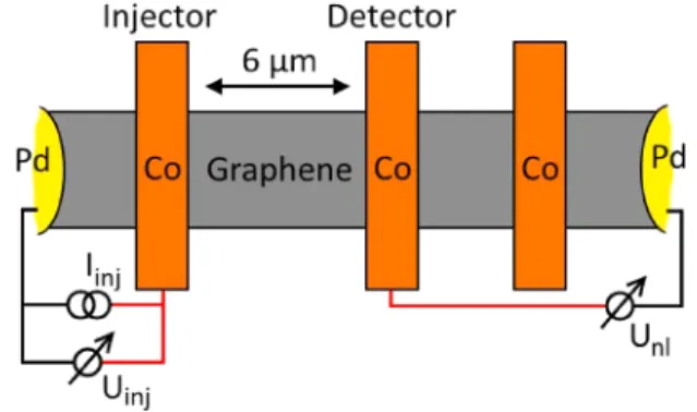
Figure 1 shows a schematic picture of the graphene flake and the non-local measurement setup. We use exfoliated sin- gle layer graphene on p
þþSi/SiO
2, where the highly doped silicon serves as a back gate, using the 285 nm thick SiO
2as a dielectric. The inner contacts are Co with 1.4 nm of MgO as a tunnel barrier, and the end contacts are Pd. More details on fabrication and spin transport properties of this device can be found in Ref. 18. At the injector electrode, a DC cur- rent bias I
injis applied and the bias voltage U
injis simulta- neously measured. We use the well-known non-local detection scheme
19to record a non-local voltage signal U
nland the corresponding non-local resistance R
nl¼ U
nl/I
injat the detector electrode. We define the outer Pd electrode as ground for the injector circuit. A positive U
injor I
injtherefore means an electron current flowing from graphene to the Co electrode. Similarly, the detector circuit is connected with the positive terminal of the nanovoltmeter to the Co detector electrode. Since we are using a DC setup, the bias depen- dence can be studied in this experiment, at the expense of sensitivity to unavoidable magnetic induction signals. The spin valve signal DR
nlis defined as DR
nl¼ R
nl,PR
nl,AP, for R
nlin the parallel (P) or antiparallel (AP) configuration. All measurements were performed at T ¼ 200 K in a cryostat equipped with a 3D vector magnet. At a distance between
FIG. 1. Sample schematic showing a graphene flake with contacts in the non-local spin valve measurement setup. The polarity of the current source and voltage detectors is indicated by red (positive) and black (negative) leads.
a)
Electronic mail: jonathan.eroms@ur.de
0003-6951/2018/113(13)/132403/5/$30.00
113, 132403-1Published by AIP Publishing.
the injector and the detector contacts of 6 lm, we achieve a spin valve signal of R
nl7 X at an injector current of I
inj¼ þ5 lA, as can be seen in Fig. 2. The resistance area prod- ucts of the injector and detector electrodes are 45.9 kX lm
2and 27.0 kX lm
2, respectively. In Fig. 3, we see in black a back gate sweep of the graphene sheet resistance, with the Dirac point at V
g¼ 2 V. From these data, the carrier mobil- ity was calculated to be between l ¼ 3500 and 5000 cm
2/V s, depending on back gate voltage. The red trace in Fig. 3 displays the gate dependence of the spin valve signal, at an injector current of I
inj¼ þ4 lA. At this injector current, the gate dependence follows qualitatively the shape for high quality tunnel contacts as described by Han et al.
20The dif- ferential resistance dR ¼
dUdIinjinj
of the injector contact is shown in the inset of Fig. 3 and displays clearly non-ohmic behav- ior, another indicator for high quality tunnel barriers.
Now, we apply a negative bias current of I
inj¼ 4 lA.
Surprisingly, the observed polarity of the spin valve signal
now depends on the gate voltage V
g, as shown in Fig. 4 (insets). When we fix the electrode magnetization to either P or AP and record the gate reponse of R
nl, we observe the black (P) and red (AP) curves in Fig. 4. The traces cross, which indicates that the back gate can change the polarity of the detected spins.
The transition between these two states is best observed in Fig. 5 which displays the gate dependence of the non-local spin valve signal DR
nl, calculated from the data in Fig. 4. A positive DR
nlthen represents the expected spin valve signal while a negative DR
nlsignifies an inverted spin valve signal.
As can be seen, the transition between regular and inverted spin signal occurs at V
g¼ 2 V. The transition is continuous and approximately linear. That the Dirac point is at the same back gate voltage as the spin neutrality point is a coin- cidence. Applying a different injector current will move the spin neutrality point, as shown below. As Fig. 5 shows, at negative bias, the sample acts as a spin field effect transistor, where the back gate can be used to turn DR
nlon, off, or invert it.
Finally, we study the bias dependence of the spin valve signal. Figure 6(a) displays the dependence of DR
nlon the injector bias U
injat a gate voltage of V
g¼ 30 V (black squares) and V
g¼ 30 V (red triangles). The inset shows the
FIG. 2. Spin valve signal at
Vg¼0 V with illustrations to show the parallel (P) and antiparallel (AP) magnetic orientation of the electrodes. The distance of the injector and detector contacts was 6
lm with an injector current ofIinj¼ þ5lA. The grey trace shows the preparation of the electrodes that was
done at a higher sweep rate, which induces a slight inductive offset because of the DC measurement setup.
FIG. 3. Gate dependence of the non-local spin valve signal
DRnlwith an injector current of
Iinj¼ þ4lA (red) and the sheet resistance (black). TheDirac point is at
Vg¼ 2 V. The inset shows the differential resistance ofthe injector tunnel contact as a function of voltage bias.
FIG. 4. Gate dependence of the non-local resistance of parallel (P, black) and antiparallel (AP, red) configurations, at a fixed injector current of
Iinj¼ 4lA. Insets show the spinvalve signal atVg¼
30 V and
Vg¼ 30 V.FIG. 5. Gate dependence of the non-local spin valve signal
DRnlat a fixed injector current of
Iinj¼ 4lA in black.132403-2 Ringer
et al.Appl. Phys. Lett.
113, 132403 (2018)U
inj-I
injdependence of the injector contact for the corre- sponding gate voltages. Figures 6(b) and 6(c) display the direct response of the detector voltage U
nlto the injector bias U
inj, for V
g¼ 30 V in Fig. 6(b) and V
g¼ 30 V in Fig. 6(c).
As Fig. 6(a) shows, for positive U
inj, DR
nlis always positive, while at negative U
inj, DR
nlchanges sign at a certain value of U
inj. This inversion point can be tuned by the gate voltage, or, equivalently, an injector bias of U
inj150 mV sets the operating point for gate-controlled spin transistor action. As the measurements are performed in a lateral spin valve geometry, we need to distinguish between contributions from the spin channel and contributions from the tunnel con- tacts. As the spin valve inversion is only enabled by a nega- tive injector current, this is a clear indicator of a contact effect. However, when applying a back gate voltage, contri- butions from the spin channel to the amplitude of DR
nlcan- not be excluded. We note that the gate dependence of the spin injection polarization can pose a problem when a mea- surement of DR
nl(V
g) is used to extract spin transport param- eters of the graphene channel.
21,22What is the mechanism behind the observed reversal of the spin polarization? The reversal of the spin polarization originates from a property of the injector contact and appears at an injector bias of U
inj150 mV. The ability to
unlikely as in our samples the MgO/Co layers are polycrys- talline. A further possible origin is defects in the barrier, where resonant tunneling at a specific energy can result in spin valve inversion.
25This does not match with the feature- less bias dependence in our sample as shown in Fig. 6.
When in contact with a ferromagnet, the band structure of graphene can be spin split through a magnetic proximity effect.
26This can then lead to an inverted spin valve when tunneling from p to n doped graphene, as observed by Asshoff et al.
11and Xu et al.
27However, due to the thick MgO barrier in our case—as evidenced by the non-ohmic differential resis- tance shown in Fig. 3—there is no region of direct contact between Co and graphene, making this explanation unlikely.
Finally, we discuss the spin polarization of the Co injectors.
While the polarization P
Nderived from the spin-resolved den- sity of states (DOS) of cobalt
28remains constant in an energy window of about 700 meV below the Fermi level, for spin injection, one has to consider the spin polarization weighted by v
a, where v is the electron velocity, and a ¼ 1 or 2 for a ballistic or diffusive situation, respectively.
29Mazin calcu- lated this quantity for Fe and Ni, showing a sign change of P
Nv2around the Fermi level for Nickel, fundamentally differ- ent from P
Nof Ni, while for Fe, both P
Nv2and P
Nshow simi- lar behavior around E
F.29
The quantities P
N, P
Nv, and P
Nv2were calculated for Co/graphene by Sipahi et al.
30They observe that, while P
Nin the bulk Co layers retains its sign over a wide energy range, the velocity-weighted polarization can show a strong energy dependence, making this a possible explanation for the observed effect. Furthermore, the spin polarization can be quite different at the interface, depending on its detailed conditions.
31Lou et al. reported a strong bias dependence in a Fe/GaAs spin valve device, offering the band structure at the Fe/GaAs as a possible explanation.
32For our situation, the relevant interface is the Co/MgO interface.
Unfortunately, due to the unknown crystal structure in our non-epitaxial samples, a comparison to first-principles calcu- lations
33is not meaningful.
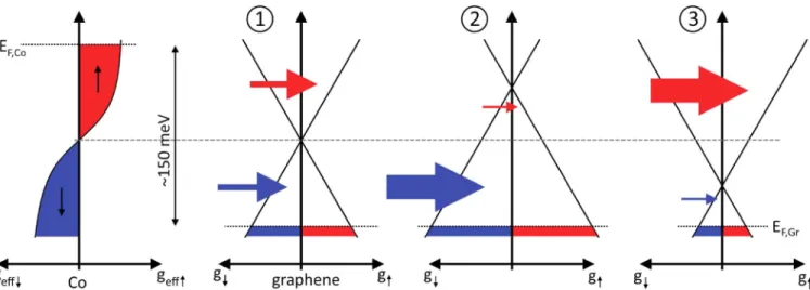
Given that reversal of spin polarization was reported in Co-graphene devices with both MgO
15,34and hBN tunnel barriers
13,14,34for negative injector bias in the range of order 100 mV, we assume that indeed the effective spin polariza- tion g
effof the tunnel current from Co into graphene has a sign change slightly below the Fermi level, as shown in Fig. 7. While the uncovered graphene regions show almost no doping (cf. resistance curve in Fig. 3), both the difference in work function of Co and graphene and the electric field
FIG. 6. (a) Plot of the spinvalve signal
DRnlin dependence of the injector
bias for
Vg¼30 V (black squares) and
Vg¼ 30 V (red triangles). Negativevalues indicate an inverted spin valve. The injector current was varied
between 0.5 and 6
lA with steps of 0.5lA for each current polarity and gatevoltage. (b) and (c) Plot of the bias measured at the detector electrode in
dependence of the injector bias for parallel (P, black) and antiparallel (AP,
red) configurations, for gate voltages of (b)
Vg¼30 V and (c)
Vg¼ 30 V.induced by the bias voltage can lead to a different position of the Fermi level underneath the Co electrodes. Assuming p- doping of the graphene underneath the contacts, an applied bias voltage of 150 mV then leads to equal amounts of electrons with negative and positive spin polarization enter- ing graphene, thus cancelling the spin signal [situation (1) in Fig. 7]. When a gate voltage is applied, the position of the Dirac point in graphene is changed, while the bias voltage fixes the separation of the Fermi levels in Co and graphene, respectively. Since the DOS in graphene strongly changes around the Dirac point, shifting the Dirac cone up or down will select either preferentially down spins [situation (2)] or up spins [situation (3) in Fig. 7], leading to the observed inversion of the spin signal. The signal is inverted for a larger proportion of down spins entering graphene, which is favored by a Fermi level lying deeper in the valence band of graphene (i.e., negative gate voltage), as found in the experi- ment (cf. Fig. 5). The precise position of the contact-induced doping sets the bias value of the spin neutrality point, which can explain its variation in samples prepared in different groups. For zero bias, the Fermi levels in graphene and Co are aligned, and the spin polarization of the tunneling current is only probed close to E
F. As the DOS of Co is fairly con- stant around E
F, changing the Fermi level in graphene by a gate voltage has little effect on the spin signal.
In conclusion, we report on a tunable spin polarization of injected spins through a Co/MgO/graphene contact. For a certain range of negative injector bias, the spin polarization can be controlled by the back gate, turning the device into a spin field effect transistor. We consider an energy depen- dence of the spin polarization at the Co/MgO interface as the most likely cause for the observed effect and propose a model that offers a conclusive explanation. In addition to the possible application as a spin transistor, we note that the gate dependence of the spin polarization has to be taken into account when studying the correlation of the spin lifetime to other gate dependent parameters of graphene.
During the preparation of this manuscript, Zhu et al.
34published a systematic study of the bias-dependent spin polarization reversal in Co/MgO/graphene and Co/hBN/
graphene tunnel junctions. They did investigate the gate dependence but did not observe an effect of comparable magnitude as in our sample.
Financial support by the Deutsche Forschungsgemeinschaft (DFG) within the Programs SFB 689 and GRK 1570 is gratefully acknowledged, as well as financial support by the Elitenetzwerk Bayern. The authors would like to thank F.
Volmer for crucial advice on improving the quality of our MgO tunnel barriers and K. Zollner and J. Fabian for discussions.
1
I. Zutic´, J. Fabian, and S. Das Sarma, Rev. Mod. Phys.
76, 323 (2004).2
S. Datta and B. Das, Appl. Phys. Lett.
56, 665 (1990).3
B. Behin-Aein, D. Datta, S. Salahuddin, and S. Datta, Nat. Nanotechnol.
5,266 (2010).
4
H. Dery, H. Wu, B. Ciftcioglu, M. Huang, Y. Song, R. Kawakami, J. Shi, I. Krivorotov, I. Zutic´, and L. J. Sham, IEEE Trans. Electron Devices
59,259 (2012).
5
H. C. Koo, J. H. Kwon, J. Eom, J. Chang, S. H. Han, and M. Johnson, Science
325, 1515 (2009).6
N. Tombros, C. J ozsa, M. Popinciuc, H. T. Jonkman, and B. J. van Wees, Nature
448, 571 (2007).7
M. Sharma, S. X. Wang, and J. H. Nickel, Phys. Rev. Lett.
82, 616 (1999).8
J. M. De Teresa, A. Barth el emy, A. Fert, J. P. Contour, F. Montaigne, and P. Seneor, Science
286, 507 (1999).9
C. Tiusan, F. Greullet, M. Hehn, F. Montaigne, S. Andrieu, and A. Schuhl, J. Phys.: Condens. Matter
19, 165201 (2007).10
F. Godel, M. Venkata Kamalakar, B. Doudin, Y. Henry, D. Halley, and J.- F. Dayen, Appl. Phys. Lett.
105, 152407 (2014).11
P. U. Asshoff, J. L. Sambricio, A. P. Rooney, S. Slizovskiy, A.
Mishchenko, A. M. Rakowski, E. W. Hill, A. K. Geim, S. J. Haigh, V. I.
Fal€ eo, I. J. Vera-Marun, and I. V. Grigorieva, 2D Mater.
4, 031004 (2017).12
A. Dankert, R. S. Dulal, and S. P. Dash, Sci. Rep.
3, 3196 (2013).13
M. V. Kamalakar, A. Dankert, P. J. Kelly, and S. P. Dash, Sci. Rep.
6,21168 (2016).
14
M. Gurram, S. Omar, and B. J. van Wees, Nat. Commun.
8, 248 (2017).15
W. Han, K. McCreary, K. Pi, W. Wang, Y. Li, H. Wen, J. Chen, and R.
Kawakami, J. Magn. Magn. Mater.
324, 369 (2012).16
W. Han, W. H. Wang, K. Pi, K. M. McCreary, W. Bao, Y. Li, F. Miao, C.
N. Lau, and R. K. Kawakami, Phys. Rev. Lett.
102, 137205 (2009).17
A. Dankert and S. P. Dash, Nat. Commun.
8, 16093 (2017).18
S. Ringer, S. Hartl, M. Rosenauer, T. V€ olkl, M. Kadur, F. Hopperdietzel, D. Weiss, and J. Eroms, Phys. Rev. B
97, 205439 (2018).19
M. Johnson and R. H. Silsbee, Phys. Rev. Lett.
55, 1790 (1985).20