Terahertz ratchet effects in graphene with a lateral superlattice
P. Olbrich,1J. Kamann,1M. K¨onig,1J. Munzert,1L. Tutsch,1J. Eroms,1D. Weiss,1Ming-Hao Liu (),1L. E. Golub,2 E. L. Ivchenko,2V. V. Popov,3,4,5D. V. Fateev,3K. V. Mashinsky,4F. Fromm,6Th. Seyller,6and S. D. Ganichev1,*
1Physics Department, University of Regensburg, 93040 Regensburg, Germany
2Ioffe Institute, 194021 St. Petersburg, Russia
3Institute of Radio Engineering and Electronics (Saratov Branch), 410019 Saratov, Russia
4Saratov State University, 410012 Saratov, Russia
5Saratov Scientific Center of the Russian Academy of Sciences, 410028 Saratov, Russia
6Technical University of Chemnitz, 09111 Chemnitz, Germany (Received 27 October 2015; published 12 February 2016)
Experimental and theoretical studies on ratchet effects in graphene with a lateral superlattice excited by alternating electric fields of terahertz frequency range are presented. A lateral superlattice deposited on top of monolayer graphene is formed either by periodically repeated metal stripes having different widths and spacings or by interdigitated comblike dual-grating-gate (DGG) structures. We show that the ratchet photocurrent excited by terahertz radiation and sensitive to the radiation polarization state can be efficiently controlled by the back gate driving the system through the Dirac point as well as by the lateral asymmetry varied by applying unequal voltages to the DGG subgratings. The ratchet photocurrent includes the Seebeck thermoratchet effect as well as the effects of “linear” and “circular” ratchets, sensitive to the corresponding polarization of the driving electromagnetic force. The experimental data are analyzed for the electronic and plasmonic ratchets taking into account the calculated potential profile and the near field acting on carriers in graphene. We show that the photocurrent generation is based on a combined action of a spatially periodic in-plane potential and the spatially modulated light due to the near-field effects of the light diffraction.
DOI:10.1103/PhysRevB.93.075422
I. INTRODUCTION
Graphene has revealed fascinating phenomena in a number of experiments owing to specifics of the electron energy spectrum resembling that of a massless relativistic particle [1–5]. Unique physical properties of graphene, such as the gapless linear energy spectrum, pure two-dimensional (2D) transport, strong plasmonic response, and comparatively high mobility at room temperature, open the prospect of high-speed electronics and optoelectronics, in particular, fast and sensitive detection of light for a range of frequencies from ultraviolet to terahertz (THz). Different mechanisms, by which the detection can be accomplished, include (i) photoconductivity due to bolometric and photogating effects [6–8], (ii) photothermo- electric (Seebeck) effect [9], (iii) separation of the photoin- duced electron-hole pairs in a periodic structure with two dif- ferent metals serving as contacts to graphene [10,11] (double comb structures) or ap-njunction [12], and (iv) excitation of plasma waves in a gated graphene sheet [13,14] (for reviews, see [15–21]). As we show in the following, graphene-based detectors may operate applying ratchet effects excited by THz radiation in a 2D crystal superimposed by a lateral periodic metal structure. The ratchet effect is of very general nature:
The spatially periodic, noncentrosymmetric systems being driven out of thermal equilibrium are able to transport particles even in the absence of an average macroscopic force [22].
This effect, so far demonstrated for semiconductor quantum wells with lateral noncentrosymmetric superlattice structures [23–30], promises high responsivity, short response times, and even new functionalites, such as all-electric detection of the
*sergey.ganichev@physik.uni-regensburg.de
radiation polarization state including radiation helicity being so far realized applying photogalvanics [31,32]. Most recently, electronic and plasmonic ratchet effects have been considered theoretically in Refs. [33–38] supporting the expected benefit of graphene-based detectors.
In this work, we report on the experimental realization and systematic study of graphene ratchets in both (i) epitaxially grown and (ii) exfoliated graphene with an asymmetric lateral periodic potential. The modulated potential has been obtained by fabrication of either a sequence of metal stripes on top of graphene or interdigitated comblike dual-grating-gate (DGG) structures. We demonstrate that THz laser radiation shining on the modulated devices results in the excitation of a direct electric current being sensitive to the radiation’s polarization state. The application of different electrostatic potentials to the two different subgratings of the dual-grating-gate structure and variation of the back gate potential enables us to change in a controllable way the degree and the sign of the structure asymmetry as well as to analyze the photocurrent behavior upon changing the carrier type and density. These data reveal that the photocurrent reflects the degree of asymmetry induced by different top gate potentials and even vanishes for a symmetric profile. Moreover, it is strongly enhanced in the vicinity of the Dirac point. The measurements together with a beam scan across the lateral structure prove that the observed photocurrent stems from the ratchet effect. The ratchet current consists of a few linearly independent contributions including the Seebeck thermoratchet effect as well as the “linear” and
“circular” ratchets, sensitive to the corresponding polarization of the driving electromagnetic force. The results are analyzed in terms of the theory of ratchet effects in graphene structures with a lateral potential including the electronic and plasmonic mechanisms of a photocurrent in periodic structures. We
show that the ratchet photocurrent appears due to the non- centrosymmetry of the periodic graphene structure unit cell.
The experimental data and the theoretical model are discussed by taking the calculated potential profile and near-field effects explicitly into account.
II. SAMPLES AND METHODS
We study the ratchet photocurrents in two different types of structures. The superlattices of the first type are fabricated on large-area graphene grown by high-temperature Si sublimation of semi-insulating SiC substrates [39,40]. This type of sample with the superlattice covering an area of about 1×1 mm2 on a graphene layer with a total area of about 5×5 mm2 allowed us, on one hand, to scan the laser beam across the superlattice and, on the other hand, to examine the photocurrent in directions along and perpendicular to the metal stripes. All samples are made from the same wafer of SiC. To obtain defined graphene edge,s we removed an edge trim of about 200μm width [see Fig.1(c)] by reactive ion etching with an argon/oxygen plasma. The carrier mobility μ=1800 cm2/Vs and residual hole density 5.3×1011cm−2 in graphene resulting in a carrier transport relaxation time τ =16 fs were measured atT =200 K. Before fabricating the superlattice structure, we carefully checked that the symmetry of the pristine graphene is unaffected by steps (terraces), which
20 x 20 µm² d = 6 µm
1 x 1 mm²
p-Si
SiO2 SiC
a1 a2
Ti/Au Al2O3
TG1 TG2
d = 3 µm (a)
Graphene (b)
(c)
(d)
(e)
(f )
1
2 3
4
5 6
S D
2
1 d1 d2
a2
a1
d2d1
Sample #A Sample #B
x y
x y
Graphene flake
w
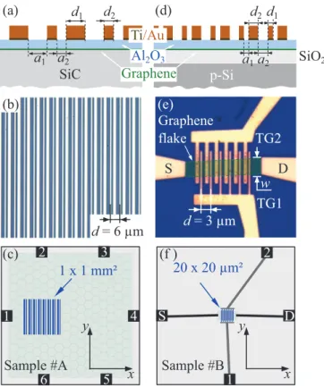
FIG. 1. Cross section, photograph and sample geometry sketch of (a)–(c) metal finger structure deposited on a large-area epitaxial graphene (sample #A) and (d)–(f) interdigitated grating gates de- posited on the exfoliated monolayer graphene flake (sample #B).
Here, d1,2 anda1,2 are the width of metal stripes and the spacing in-between, respectively. The superlattice period isd=d1+d2+ a1+a2.
may be formed on the SiC surface. For that, we studied the THz radiation-induced photocurrent and ensured that it vanishes at normal incidence [41–43]. As a further step, we deposited an insulating aluminium oxide layer on top of the graphene sheet. For this purpose, we first deposited a thin (<1 nm) Al seed layer by evaporation in ultrahigh vacuum and oxidized it subsequently. Then, we prepared 26 nm layer of aluminum oxide Al2O3with atomic layer deposition using H2O and trimethyl aluminum as precursors. The lateral periodic electrostatic potential is created by micropatterned periodic grating-gate fingers fabricated by electron beam lithography and subsequent deposition of metal (5 nm Ti and 60 nm Au) on graphene covered by Al2O3. A sketch of the gate fingers and a corresponding optical micrograph are shown in Figs.1(a)and1(b), respectively. The grating-gate supercell consists of two metal stripes having different widths d1=2 μm andd2=1 μm separated by different spacings a1=2 μm and a2=1 μm. This supercell is repeated to generate an asymmetric periodic electrostatic potential [24,44]
(periodd=d1+a1+d2+a2=6μm) superimposed upon graphene [see Fig. 1(b)]. The 1×1 mm2 area grating-gate structure is located on the left half of the sample so that a large graphene area remains unpatterned [see Fig. 1(c)]. For the THz beam of 1.5 mm diameter, this design allows us to study the photocurrent excited in either the superlattice structure or the unpatterned graphene reference area. Contact pads were placed in a way that the photoinduced currents can be measured parallel (jy, contacts 2 and 6) and perpendicular (jx, contacts 1 and 4) to the metal fingers. Two additional contacts (3 and 5) were used for detecting the photocurrent signals from the unpatterned area as a reference.
The structures of the second type are fabricated on small- area graphene flakes [1]. The benefit of these types of structures is the possibility to apply different bias voltages to the individual subgrating gates forming the superlattice allowing us to explore the role of the asymmetry of the lateral periodic electrostatic potential in the photocurrent formation as well as to examine the ratchet effects in the vicinity of the Dirac point. The graphene layers were prepared by mechanical exfoliation of natural graphite onto an oxidized silicon wafer.
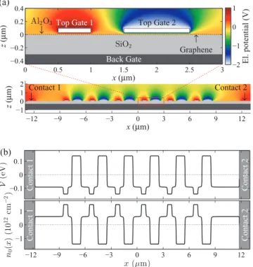
The samples used in this study were all single-layer flakes. The periodic lateral electrostatic potential is created by 5 nm/60 nm Ti/Au interdigitated metal-grating gates deposited on top of the graphene layer [see Figs. 1(d)–1(f)], applying the method described above. The insulating layer of aluminum oxide is used to separate the grating gates and graphene. The asymmetric lateral structure incorporates the interdigitated dual-grating gates (DGG) TG1 and TG2 having different stripe width and stripe separation. An optical micrograph of the interdigitated grating gates is shown in Fig.1(e). The supercell of the grating-gate fingers consists of metal stripes having two different widthsd1=0.5μm andd2 =1 μm separated by spacings a1 =0.5 μm and a2=1 μm [Fig. 1(d)]. This asymmetric supercell is repeated six times to create a periodic asymmetric potential (periodd =3μm) [Fig.1(e)]. The two subgrating gates, each formed by fingers of identical width, can be biased independently. Therefore, the asymmetry of the lateral potential of the DGG structure can be varied in a controllable way. Figure2shows the potential profile obtained by a 2D finite-element-based electrostatic simulation using
x (μm) z (μm) Contact 1
↓
Contact 2
↓
−12 −9 −6 −3 0 3 6 9 12
−1 0 1
2 x (μm)
z (μm)
↑ Graphene SiO2
Al2O3
↓ Top Gate 1 Top Gate 2 Back Gate (a)
0 0.5 1 1.5 2 2.5 3
−0.4
−0.2 0 0.2 0.4
El. potential (V)
−2
−1 0 1
Contact 1 Contact 2
x(µm) n0(x)(1012cm−2)
−12 −9 −6 −3 0 3 6 9 12
−1 0 1
V(eV) Contact 1 Contact 2
(b)
−0.1 0 0.1
FIG. 2. (a) Modeled DGG device (sample type #B) geometry showing the spatial distribution of the electrostatic potential ob- tained by 2D finite-element simulation, considering gate voltages (UTG1, UTG2)=(1,−2) V as an example. (b) Extracted equilibrium free-carrier density profile in graphene (lower panel, positive carrier density corresponds to electrons and negative carrier density corre- sponds to holes in graphene) and the corresponding local energy band offset (upper panel) assuming a uniform back gate contribution with voltageUBG=10 V as an example. We use the energy units for the electrostatic potential in this paper.
FENICS [45] and GMSH [46] for the device geometry of the experiment. The profile of this potential was found by solving the Poisson equation taking into account its screening by the carriers in graphene and the quantum capacitance effect [47–49]; see AppendixAfor details. The samples were glued onto holders with conductive epoxy utilizing the highly doped silicon wafer as a back gate which enabled us to change type and density of free carriers in graphene.
The experiments were performed using a continuous wave (cw) methanol laser [50–52] emitting at the frequency f=2.54 THz (wavelength ofλ=118μm and photon energy ω=10.5 meV). The radiation powerP, being of the order of 50 mW at the sample surface, has been controlled by pyroelec- tric detectors and focused onto samples by a parabolic mirror.
The beam shape of the THz radiation is almost Gaussian, checked with a pyroelectric camera [53,54]. The peak intensity in the laser spot on the sample, being of about 1.5 mm diameter [55,56], wasI ≈8 W/cm2. The THz radiation polarization state was varied by rotation of crystal quartz λ/4 and λ/2 plates [57,58]. To obtain circular and elliptically polarized radiation, the quarter-wave plate was rotated by an angle ϕ between the initial polarization plane and the optical axis of the plate. The radiation polarization states for several anglesϕ are illustrated on top of Fig.3. The orientation of the linearly polarized radiation is defined by the azimuthal angleαwith
-4 0 4 8
Angleϕ
0 45˚ 90˚ 135˚ 180˚
Sample #A
f= 2.54THz
σ+ σ-
RL V2-6 V3-5
Pos.1 Pos.2 x
z y
[V2-6(ϕ) - V2-6(0)] / P (arb. units)
FIG. 3. PhotovoltageV2-6(ϕ)−Voff measured in sample #A for the laser spot focused on patterned graphene, position 1. The signal is plotted as a function of the angle ϕ defining the radiation polarization state. The ellipses on top illustrate the polarization states for several values ofϕ. Solid curve shows the fit according V2-6(ϕ)−Voff=VCsin 2ϕ+VL1(sin 4ϕ)/2 [see also Eqs. (8) and (9) and the corresponding discussion in the text]. Dashed and dotted-dashed curves show individual contributionsVCsin 2ϕ and VL1(sin 4ϕ)/2, respectively. Arrows indicate anglesϕcorresponding to right-handed (σ+) and left-handed (σ−) circularly polarized radiation.
α = ϕ = 0 chosen in such a way that the electric field of the incident linearly polarized radiation is directed along thex direction, i.e., perpendicular to the metal fingers. The ratchet photocurrents have been measured in graphene structures at room temperature as a voltage drop across a 50-or 470- load resistance RL. The photovoltage signal is detected by using standard lock-in technique. The photocurrentIrelates to the photovoltageV asI =V /RLbecause in all experiments described below the load resistance was much smaller that the sample resistance RS (RLRS). The corresponding photocurrent density is obtained asj =I/w, wherewis the width of the two-dimensional grating-gate structure being 1 mm for samples type #A and 5μm for samples type #B.
III. EXPERIMENTAL RESULTS
A. Photocurrents in large-area epitaxial graphene structures First, we discuss the results obtained from the large- scale lattice prepared on the top of epitaxial graphene layer.
Irradiating the structure with the THz beam, position 1 in Fig. 3, we detected a polarization-dependent photocurrent.
Figure 3 shows the corresponding photovoltage V ∝jy, measured in the direction along the metal fingers (y direc- tion) as a function of the angle ϕ governing the radiation ellipticity. The signal varies with the radiation polarization asV2-6(ϕ)−Voff=VCsin 2ϕ+VL1(sin 4ϕ)/2, where Voff is a polarization-independent offset which is obtained asV2-6at ϕ=0 [59]. The figure reveals that the signal is dominated by the circular photocurrentjC∝VC being proportional to the degree of circular polarizationPcirc=sin 2ϕand reversing its direction by inverting of the THz radiation helicity. The second contribution to the signalVL1∝jL1, whose amplitude is about three times smaller than VC, corresponds to the
V C ( µV / W ) 0.5
0.0 1.0
Spot position, l(mm) Sample #A
1
0 2
f = 2.54 THz l 0 1.0 2.5
3 RL
spot
structure
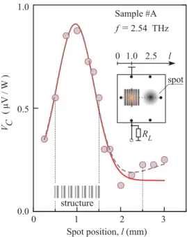
FIG. 4. Circular photocurrentjC∝VCin sample #A as a function of the laser spot position. The laser spot is scanned along the x direction and the photocurrent is picked up from contacts 2-6 allowing to probe current in theydirection (see top right inset). The solid line represents the response calculated assuming that the signal stems from the lateral structure only and using the laser beam shape measured by the pyroelectric camera. The curve is scaled to the photocurrent maximum. Dashed line is a guide for the eye. The bottom inset shows schematically the grating-gate position.
photocurrent driven by the linearly polarized radiation and vanishes for circularly polarized radiation. In experiments applying half-wave plates it varies with the azimuth angle α as V2-6(α)−Voff=VL1sin 2α (not shown). Note that the functions (sin 4ϕ)/2 and sin 2αdescribe the degree of linear polarization of THz electric field in the coordinate framex,y rotated by 45◦in respect to thex,yaxes [25]. Our experiments were performed on several identically patterned samples.
Although they were processed and structured identically, we observe different ratios of the linear and circular components for the same wavelength. As we show in the following, this fact can be attributed to slightly different intrinsic transport relaxation times (charge-carrier mobilities) in the samples.
Shifting the beam spot away from the structured area, position 2 in Fig. 3, and measuring the signal either from contacts 2-6 or 3-5, we observe the signal reduced by an order of magnitude. This observation indicates that the photocurrent stems from the irradiation of the superlattice. To provide additional evidence for this conclusion, we scanned the laser spot across the sample along thexdirection. The photocurrent was measured between contacts 2 and 6 aligned along the metal stripes, i.e., along the y direction. The experimental geometry and the circular photocurrentjC∝VCas a function of the radiation spot position l are shown in Fig. 4. The current reaches its maximum for the laser spot centered at the superlattice and rapidly decays with the spot moving away.
Comparison of VC(x) with the curve calculated assuming that the signal stems from the lateral structure only and by using the laser beam spatial distribution measured by
Sample #B
=-20 V UBG
= 0 UTG
0˚ 45˚ 90˚ 135˚ 180˚
Azimuthal angle, α Vx(arb.units)norm
1
0
-1
f= 2.54THz
RL Vx x z y hω
Sample #A
FIG. 5. Normalized photosignalVxnorminduced by linearly polar- ized radiation in the large epitaxial sample #A and DGG graphene sample #B in thexdirection normal to the metal stripes. Arrows on top show the polarization plane orientation for several anglesα. The data for the DGG sample #B are obtained forUTG1=UTG2=0 andUBG=
−20 V. Solid curves show fit according toVxnorm=V0+VL2cos 2α [see also Eq. (7) and the corresponding discussion in the text].
a pyroelectric camera shows that the signal follows this curve. This observation unambiguously demonstrates that the photocurrent is caused by irradiating the superlattice. It also excludes photocurrents emerging due to possible radiation- induced local heating causing the Seebeck effect, as such a signal should obviously reverse its sign at the middle of the sample. The only deviation from this behavior is detected for large values of l at which the signal starts growing again. This result is attributed to the generation of the edge photocurrents reported in Refs. [43,56]. For large-lvalues, the beam spot reaches the edge of the graphene sample, resulting in a photocurrent caused by the asymmetric scattering at the graphene edge [56]. The ratchet photosignalV1-4∝jxis also observed in the direction perpendicular to the fingers, i.e., along thexdirection. In this case, the signal is insensitive to the THz electric field handedness and varies only with the degree of linear polarization as V1-4=V0+VL2(cos 4ϕ+1)/2 or V1-4=V0+VL2cos 2α(see Fig.5showingV1-4as a function of the azimuthal angle α). The same dependence has been measured in the DGG device, sample #B in Fig.5, indicating that the DGG structure features the same superlattice effect as the large-area one (sample #A). As we show in the following, the appearance of the photocurrent along and across the periodic structure as well as its polarization dependence are in full agreement with the ratchet effects excited by polarized THz electric field in asymmetric lateral superlattices. The overall qualitative behavior of the photocurrent is also in agreement with that of the electronic ratchet effects observed in semiconductor quantum well structures with a lateral su- perlattice [23–25]. So far, the properties of graphene were not manifested explicitly. The Dirac fermion properties of charge carriers in graphene manifest themselves in superlattices of type #B with independently controlled gates.
B. Photocurrents in interdigitated dual-grating-gates graphene structures
The ratchet effects are expected to be strongly dependent on the in-plane asymmetry of the electrostatic potential and
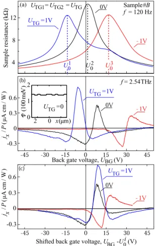
FIG. 6. Back gate voltage dependencies obtained for the top subgate voltagesUTG1=UTG2=UTG. (a) Two-terminal resistance of the DGG structure #B. (b) Photocurrent jx(α=0)=j0+jL2
normalized by the radiation intensity. Inset shows the energy band offset profiles at UTG=0 and UBG= −20 V. (c) Photocurrent jx(α=0) normalized by the radiation intensity as a function of the relative gate voltageUBG−Um,i, whereUm,i is defined as the back gate voltage for which the resistance is the largest at corresponding UTG[see panel (a)].
near-field effects of the radiation diffraction [25,33,34,38].
To demonstrate the effect of the asymmetry and exam- ine the ratchet effects in the vicinity of Dirac point, we studied samples with an interdigitated dual-grating structure [see Figs. 1(d)–1(f)]. In the DGG structures, the degree of asymmetry can be controllably varied by applying different potentials to the top grating gates. Moreover, using the back gate voltage UBG, we can globally change the background carrier density in the graphene flake. When the top gates are both grounded, the resistance exhibits one maximum upon tuning the back gate voltage. The maximum corresponds to the Dirac point and is detected close to zero voltage, which confirms low residual doping of graphene [Fig.6(a)]. When we apply a voltage to the top gates, the back gate voltage corresponding to the Dirac point is shifted due to stray coupling of the top grating gates into the entire graphene. Furthermore, the top gates strongly modulate the carrier density in graphene directly underneath them, leading to an additional weak resistance maximum in the back gate response. Applying voltages of different polarity to different top grating gates
results in a superpostition of resistance maxima corresponding to the Dirac points underneath and between the gate fingers (not shown here). We observe a slight hysteresis in the back gate sweep (shift of the resistance maximum position by UBG≈5 V), which is probably due to the measurement being performed in the ambient air. When we set the TG1 voltage to UTG1= −2 V and TG2 voltage toUTG2= +2 V, we observe a splitting of the Dirac peak into three peaks (not shown), corresponding to regions with three different carrier densities:
underneath the top gates TG1 and TG2 and in-between the gate stripes, respectively.
Due to technological reasons (presence of the subgrating gates), the photocurrent in DGG structures can be exam- ined only in source-drain direction, i.e., normal to the gate stripes [60]. In the following experiments aimed to study the photocurrent jx(α=0)=j0+jL2 as a function of the back gate voltage for differently biased top gates we used the THz radiation polarized along the source-drain direction.
Figure6(b)showsjx(UBG) obtained for the three equal values of top gate voltagesUTG1 =UTG2=UTG. The photocurrent shows a complex sign-alternating behavior with enhanced magnitude in the vicinity of the Dirac points being character- ized by resistance maxima and sign inversion forUTG=0 and +1 V. The photocurrents have opposite directions at very high (aboveUBG=40 V) and at high negative back gate voltages.
Figure6(b)demonstrates that while the overall dependencies of the photovoltage obtained at different top gate potentials are very similar, they are shifted with respect to each other to that in the transport curves. This is clearly seen in Fig.6(c) where the curves for nonzero top gate voltages are shifted by the back gate voltageUm,i at which the resistance achieves maximum at correspondingUTG [see Fig. 6(a)]. The figure reveals that the current can change its sign in the vicinity of the Dirac point. This fact can naturally be attributed to the change of carrier type from positively charged holes to negatively charged electrons [61].
In order to tune the lateral asymmetry, we applied different bias voltagesUTG1=UTG2 to the grating subgates. Figure7 shows the photocurrentjxobtained for (i)UTG1=2 V,UTG2 =
−2 V, (ii)UTG1= −2 V,UTG2=1 V, and (iii)UTG1= −2 V, UTG2=0. For cases (i) and (ii), the potential asymmetry is efficiently inverted and hence we obtain inverted photocurrents far away from the Dirac point, i.e., at large values of UBG. These observations show that the photocurrent is caused by the excitation of the free carriers in graphene beneath the superlattice and its direction depends on the sign of the in-plane asymmetry of the electrostatic potential. More complicated behavior is detected in the vicinity of the Dirac points. Here, the polarity of the free-carrier distribution in graphene and hence that of the photocurrent strongly depend on the voltage set at the top gates. This causes a more complicated variation of the photocurrent (including its sign reversal) as a function of the back gate voltageUBGaround the Dirac point. Comparing the magnitudes of the signals for equal and unequal top gate voltages [Figs.6(b)and 7(a), respectively] we see that in the latter case the photocurrent is several times enhanced. Finally, we note that if only one of the top gates is biased, the signal vanishes for almost all back gate voltages. The calculation of the electrostatic potential indeed reveals that the potential becomes almost symmetric in this case indeed.
FIG. 7. (a) Gate voltage dependence of the photocurrentjx(α= 0)=j0+jL2 normalized by the radiation intensity measured for three sets of unequal potentials at the top gatesUTG1=UTG2. Panels (b) and (c) show, respectively, the energy band offset and carrier density atUBG= −20 V.
To summarize, experiments on two different types of graphene structures provide a self-consistent picture, demon- strating that the photocurrents (i) are generated due to the presence of asymmetric superlattices, (ii) are characterized by specific polarization dependencies for directions along and across the metal stripes, (iii) changes the direction upon reversing the in-plane asymmetry of the electrostatic potential as well as changing the carrier type, (iv) are characterized by a complex sign-alternating back gate voltage dependence in the vicinity of the Dirac point, and (v) are strongly enhanced around the Dirac point.
IV. DISCUSSION
Now, we discuss the origin of the ratchet current in graphene with an asymmetrical grating irradiated by the THz beam. The effect of the grating is twofold: (i) it generates a one-dimensional periodic electrostatic potential V(x) acting upon the 2D carriers and (ii) it causes a spatial modulation of the THz electric field due to the near-field diffraction [58].
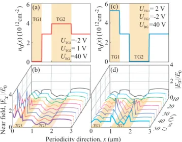
Figures8(a)and8(b)show calculated coordinate dependencies of the free-carrier density n0(x) and THz electric near-field E(x) for the DGG structure #B for two combinations of the top and back gate voltages. The electric field distribution caused by the near-field diffraction is calculated for radiation with the frequencyf =2.54 THz applying a self-consistent elec- tromagnetic approach based on the integral equation method described in detail in Ref. [62] (see also AppendixA). Figure8
x x
n0(x) n0(x)
TG1 TG2
TG1 TG2
2 G T 1 G T 2
G T 1 G T
FIG. 8. Equilibrium free-carrier density profile as a function of the coordinatex, shown for one period (d=3 μm) of the DGG sample #B. Shadowed areas indicate the positions of the metal stripes.
The data are calculated for the electrostatic potential corresponding to (a)UTG1= −2 V,UTG2=1 V,UBG=40 V, and (c)UTG1=2 V, UTG2= −2 V,UBG=40 V. Panels (b) and (d) show the corresponding near-field amplitude distribution of the radiation withf =2.54 THz for the above set of gate potentials. The near field is shown as a ratio of the amplitude of the near field|Ex|acting on graphene along the xdirection and the amplitudeE0of the electric field of the incident plane wave.
demonstrates that both the carrier density and THz field acting on charge carriers in thexdirection are asymmetric and their distribution is strongly affected by the voltages applied to the individual top gratings. These one-dimensional asymmetries result in the generation of a dc electric current. As we show in the following, the ratchet current may flow perpendicular to the metal fingers or along them. The mechanism leading to the photocurrent formation can be illustrated on the basis of the photocurrent caused by the Seebeck ratchet effect (thermoratchet). This type of the ratchet currents can be generated in the direction perpendicular to the metal stripes and corresponds to the photocurrentjxS∝V0 in Fig.5. The spatially modulated electric field of the radiation heats the electron gas changing the effective electron temperature from the equilibrium valueT toT(x)=T¯+δT(x) [63]. Here, ¯T is the average electron temperature andδT(x) oscillates along the x direction with the superlattice period d. In turn, the nonequilibrium correction δT(x) causes an inhomogeneous correction to the dc conductivityδσ(x)∝δT(x). Taking into account the space-modulated electric field (−1/e)dV/dx, we obtain from Ohm’s law the thermoratchet current in the form [33]
jxS= −1 e
dV dxδσ(x)
. (1)
Here,e <0 is the electron charge, and angular brackets denote averaging over a spatial period. This photocurrent vanishes if the temperature is not space modulated, therefore, it is called the Seebeck ratchet current [64].
Aside from the thermoratchet effect, the THz radiation can induce additional photocurrents being sensitive to the linear polarization plane orientation or to the helicity of circularly polarized photoexcitation. In the classical regime achievable in our experiments and characterized byωεFwhereεFis the Fermi energy, all these photocurrents can be well described by means of Boltzmann’s kinetic equation for the coordinate- dependent distribution function fk(x). It has the following form:
∂
∂t +vk,x ∂
∂x + F(x)
∂
∂k
fk(x)+Qk{f} =0, (2) wherevkis the velocity of an electron with the wave vectork being equal in graphene tov0k/k,v0=106m/s is the Dirac fermion velocity,Qk is the collision integral, andF(x) is the periodic force acting on charged carriers
F(x)=e[E(x)e−iωt+c.c.]−dV(x)
dx x,ˆ (3) where ˆx is the unit vector in thex direction. In terms of the distribution function, the electric current density is written as
j =4e
k
vkfk(x) , (4) where the factor 4 accounts for the spin and valley degeneracies in graphene. In the next section, we present the theory of the ratchet currents which is valid for arbitrary large and abrupt periodic electrostatic potentials V(x) and results of numerical calculations based on the developed theory and the complex distribution of the near field. However, in order not to overload the discussion of the experimental results with cumbersome equations, we first follow Refs. [23–25,33]
and present solutions of the Boltzmann equation for weak and smooth electrostatic potential and the electric near field.
Iterating the Boltzmann equation (2) for smallV(x),E(x), and their gradients, and ignoring the birefringence effect under the grating gate [65,66], we obtain the dc current density componentsjx andjy:
jx =
[χ0E2+χL(|Ex|2− |Ey|2)]dV dx
, (5)
jy=
[ ˜χL(ExEy∗+Ex∗Ey)+γi(ExEy∗−Ex∗Ey)]dV dx
. (6) For incident radiation, the combinations bilinear in the field amplitudes vary upon rotation of quarter- and half-wave plates as [66]
|Ex|2− |Ey|2=E2cos 4ϕ+1
2 =E2cos 2α, (7) ExEy∗+Ex∗Ey =E2sin 4ϕ
2 =E2sin 2α, (8) i(ExEy∗−Ex∗Ey)= −E2sin 2ϕ. (9) All photocurrent contributions are detected in experiment (see Figs. 3 and 5). The coefficient χ0 corresponds to the thermoratchet current discussed above. This photocurrent can be generated in the in-plane direction normal to the metal stripes. In experiments it yields the signalV0∝j0(see Fig.5).
The part of the signal detected for the same direction and
varying upon rotation of the linear polarization,VLP2∝jLP2 in Fig. 5, is given by the second term in the right-hand side of Eq. (5) and is proportional to χL [67]. The linear (jLP1∝VLP1) and circular (jC∝VC) photocurrents observed in the direction along the metal stripes correspond to the first and second terms in the right-hand side of Eq. (6) and describe the linear ( ˜χL) and circular (γ) ratchet effects, respectively.
The polarization-dependent contributions appear because the free carriers in the laterally modulated graphene can move in the two directions (x,y) and are subjected to the action of the two-component electric field with theExandEycomponents.
Now, we discuss the role of the superlattice asymmetry in the thermoratchet current formation. Taking the lateral- potential modulation and the electric field in the simplest form V(x)=V0cos (qx+ϕV), (10) E(x)=E0[1+hcos (qx+ϕE)], (11) withq =2π/d, we obtain for the average [33]
|E(x)|2dV dx
=qV0hE02sin (ϕE−ϕV). (12) The above phenomenological equations reveal that the ther- moratchet current can be generated only if the lateral superlat- tice is asymmetric. The asymmetry, created in our structures due to different widths of the metal fingers and spacings between them (Fig. 1), causes a phase shift between the spatial modulation of the electrostatic lateral potential gradient dV(x)/dxand the near-field intensityE2(x) yielding a nonzero space average of their product. The role of the superlattice lateral asymmetry and peculiarities of the graphene band structure are explored in the experiments on the interdigitated DGG structures. The back gate and the two independent top subgrating gates enabled us to controllably change the free-carrier density profile in thex direction. Let us begin with the data for equal top gate potentials shown in Fig.6.
At zero top gate voltages, the asymmetry is created by the built-in potential caused by the metal stripes deposited on top of graphene. Transport data reveal that at zero back gate voltage we deal with graphene almost at the charge neutrality point.
The photocurrent shows a complex behavior upon variation of the back gate voltage. First of all, it has the opposite polarities at large positive and negative back gate voltages.
This fact can be primarily attributed to the change of the carrier type in graphene which results in the reversal of the current direction. At moderate back gate voltages, the amplitude of the photocurrent substantially increases whereas in the vicinity of the Dirac point it exhibits a double sign inversion. The origin of this behavior is unclear. First of all, it may be caused by possible band-to-band optical transitions which become allowed at Dirac point because the double Fermi energy can be smaller than the photon energy in this case. Also, as mentioned in the previous section, the sign of the free-carrier distribution in graphene and hence that of the photocurrent strongly depend on the voltage set at the top gates which causes a more complex variation of the photocurrent (including a photocurrent sign reversal) as a function of the back gate voltage around the Dirac point.
Figure6demonstrates that the application of a positive or negative voltage to both top gates does not change qualitatively the photocurrent behavior but shifts the dependence as a whole to smaller or larger back gate voltages in full correlation with the shift of the charge neutrality point documented by transport measurements. These results show that the current is proportional to the charge sign of the carriers (negative for electrons, positive for holes) in graphene. Figure6(c)reveals that the photocurrent reverses its direction under inversion of the top gate voltage UTG from +1 V to −1 V. This fact is also in agreement with Eq. (5). Indeed, at small amplitude of the potential, the photocurrent is j ∝ |E(x)|2dV/dx . This average changes sign upon the inversion of the potential V(x)→ −V(x). Even a more spectacular role of the in-plane asymmetry is exhibited in the experiments on the DGG struc- ture with different polarities of the gate voltages applied to TG1 and TG2. First of all, the difference in the potentials increases the asymmetry resulting in the photovoltage enhancement by more than an order of magnitude for large positive and negative gate voltages (Figs. 6 and7). Moreover, the change of the relative polarity of the TG1 and TG2 gate voltages results in a reversed photocurrent direction for all back gate voltages clearly reflecting the sign inversion of the static potential asymmetry given bydV/dx. Figure7 also shows that for a certain combination of the top gate voltages (UTG1= −2 V and UTG2=0), the photocurrent almost vanishes. This fact will be discussed in the next section presenting calculations of the photocurrent for exact profiles of the electrostatic potential and radiation near field.
Summarizing the discussion, all experimental findings can consistently be explained qualitatively by the free-carrier ratchet effects. A quantitative analysis is presented in Sec.V.
V. THEORY
A. Photocurrent in the direction normal to the grating stripes Three microscopic mechanisms of the ratchet current are considered and compared: (i) the Seebeck contribu- tion generated in the course of the photoinduced spatially modulated heating of the free carriers accompanied by a periodic modulation of the equilibrium carrier density; (ii) the polarization-sensitive current controlled by the elastic scattering processes; and (iii) differential plasmonic drag. The main difference of the first two mechanisms as compared with those in lateral quantum-well structures [25] is determined by specific properties of graphene, namely, (i) the linear, Dirac-type, dispersion of free-carrier energy, and (ii) the degenerate statistics of the free-carrier gas in doped (or gated) graphene even at room temperature.
The photocurrent flowing in the periodicity direction is given by
jx =jxS+jxL+jplD. (13) Here, the first term is the Seebeck ratchet current. The second term is caused by pure elastic scattering processes which are not related to carrier heating [33], it yields a polarization- dependent photocurrent varying upon rotation of the radiation polarization plane. The photocurrent jplD is caused by the differential plasmonic drag [34,38].
We apply the kinetic theory for calculating the Seebeck ratchet current. For degenerate statistics it yields (see Ap- pendixB)
jxS= e3v02 π2
τ2τε
1+(ωτ)2
|E(x)|2dxd[εF−V(x)]−1 [εF−V(x)]−1 . (14) Here, τ and τε are the free-carrier momentum and energy relaxation times, respectively. The derived expression for the Seebeck ratchet current is valid for arbitrarily large and abrupt periodic potentialV(x). We assume the Fermi energy to lie high above the Dirac point and take into account only one sort of free carriers, namely, the electrons. The similar results are obtained for the Fermi energy lying deep enough in the valence band in which case the electron representation is replaced by the hole representation. Due to the charge-conjugation symmetry between electrons and holes in graphene, the current (14) reverses under the changes εF→ −εF,V(x)→ −V(x), ande→ −e, where the energy is referred to the Dirac point.
We also note that this current vanishes if the x-coordinate dependence of the near-field intensity|E(x)|2is a composite functionf[V(x)]. One more symmetry property follows for a low-amplitude potential|V(x)| εF: in this case, the current reversal occurs just at the potential inversionV(x)→ −V(x).
The differential plasmonic-drag photocurrentjplD induced in the grating-gated graphene by the normally incident THz radiation can be estimated as (see AppendixC)
jplD= −2e3v02 π2ω
τ2 1+(τ ω)2
q
q(|Eq|2− |E−q|2), (15) where Eq are the Fourier-space harmonics of the in-plane component of the near electric fieldEx(x) in graphene with q=2π l/d where l is an integer. It is worth noting that the differential plasmonic drag [38] can be also viewed phe- nomenologically as a specific “linear” ratchet effect induced in a periodic graphene structure by the normally incident THz radiation with the electric field polarized perpendicular to the grating gate.
We simulate the interaction of THz radiation incident normally upon the grating-gated graphene in the framework of a self-consistent electromagnetic approach based on the integral equation method described in detail in Ref. [62]. The calculations are performed for the characteristic parameters of the DGG structure used in the experiment (see AppendixA).
In our simulations, we assume the metal grating stripes to be perfectly conductive and infinitely thin. This is a quite justified and commonly used assumption at THz (and lower) frequencies where metals are characterized by a high real conductivity. As a result of the electromagnetic modeling, we obtain the in-plane component of the near electric field in graphene E(x)x entering Eqs. (14) and (15). Periodic electrostatic potentialV(x) in graphene is created by applying different electric voltages to the two different subgratings of the DGG. It should be noted that the periodic electrostatic potential is induced in graphene even for zero voltage at each subgrating due to finite density of states in graphene (the quantum capacitance effect). The profiles of the calculated near electric field and the free-carrier density are shown in Figs. 8(b)and8(d)for various voltages applied to different subgratings of the dual-grating gate at frequency 2.54 THz.
UBG = 40V
j x / P ( µA cm / W )
Frequency (THz)
1 2 3 4
-1.5 -1.0 -0.5 0 0.5 1.0
UTG1/UTG2 = 2V / -2V UTG1/UTG2 = -2V / 1V
Seebeck ratchet
plasmonic drag
Seebeck ratchet f = 2.54 THz
plasmonic drag
FIG. 9. Seebeck thermoratchet (solid lines) and plasmonic-drag (dashed line) photocurrents calculated forUBG=40 V applied to the DDG graphene superlattice sketched in Fig.1. Red lines show the results forUTG1=2 V andUTG2= −2 V, blue lines forUTG1= −2 V andUTG2=1 V. Red and blue dots correspond to the experimental data taken from Fig.7.
It is seen that the near electric field is asymmetric relative to equilibrium free-carrier density profile in graphene. This gives rise to the Seebeck (thermoratchet) photocurrent Eq. (14).
The calculated thermoratchet photocurrent as a function of frequency is shown by solid curves in Fig.9 for various voltages applied to different subgratings of the DGG for monopolar graphene charged by applying large positive voltage to the back gate electrode. In this situation, we deal with electrons in graphene under the metal fingers and between them even for negative voltages applied to a top gate. It is worth noting that the magnitude of the photocurrents as well as the inversion of the photocurrent direction for reversing of relative signs of voltages applied at different subgratings of the top dual-grating gate are in accordance with the experimental observations at the frequency 2.54 THz (Fig.9).
The calculated differential plasmonic-drag photocurrent (15) as a function of frequency is shown by dashed curves in Fig. 9. It follows from the figure that, as well as for the thermoratchet photocurrent, the inversion of the voltage signs at different subgratings of the top DGG changes the sign of the plasmonic-drag photocurrent. However, the plasmonic- drag photocurrent is directed oppositely to the thermoratchet photocurrent. Therefore, the plasmonic-drag photocurrent can compensate or, for a certain combination of top gate voltages, even cancel the thermoratchet photocurrent diminishing the total photocurrent generated in graphene by the incident THz radiation. This fact may be responsible for the vanishingly small photocurrent observed forUTG1 = −2 V andUTG2=0 (Fig.7).
B. Photocurrent in the direction along the grating stripes Solution of the Boltzmann equation (2) also yields they component of the photocurrent. In order to derive the expres- sion forjyfor the electrostatic potentialV(x) comparable to the Fermi energy, we assume that both energy relaxation and diffu- sion are less effective than elastic scattering:D0(π/d)2,τε−1 ω,τ−1, but the productωτcan be arbitrary. Here,D0=v20τ/2 is the diffusion constant of the Dirac fermions in graphene.
We consider the elastic scattering by a long-range Coulomb potential. In this case, the momentum relaxation time in nonstructured graphene is a linear function of the Fermi energy: τ ∝εF. Therefore, in the structures with a lateral superlattice under study we have τ(x)= τ [1−V(x)/εF].
Using the procedure described in Ref. [33], we obtain the photocurrent component along the grating stripes in the form of Eq. (6):
jy =
[ ˜χL(ExEy∗+Ex∗Ey)+γ i(ExEy∗−Ex∗Ey)]dV dx
, (16) where the coordinate dependence of the coefficients ˜χLandγ is given by
˜
χL(x)= −e3v20τ 2π2εF
τ2(x)[3+ω2τ2(x)]
1+ω2τ2(x) , γ(x)= e3v20τ
π2εF
τ(x)
ω[1+ω2τ2(x)]. (17) The coefficients ˜χL and γ describe the linear and circular ratchet effects, respectively. The linear polarization-dependent and helicity-dependent combinations of the products ExEy∗ andEx∗Eywhich determine the photocurrentjy are related to the corresponding combinations of the incident radiation as follows [65]:
Ex(x)Ey∗(x)=R(x)E0xE0y∗ .
A presence of imaginary part ImR=0 is caused by effective birefringence of the studied low-symmetry structure resulting in an ellipticity of the near-field polarization under incidence of pure circularly or pure linearly (in the framex,y) polarized radiation.
VI. CONCLUSION
To summarize, we have demonstrated that ratchet effects driven by THz electric fields can be efficiently generated in graphene with a lateral superlattice. The ratchet photocurrent includes the Seebeck thermoratchet effect as well as the effects of “linear” and “circular” ratchets, sensitive to the corresponding polarization of the driving electromagnetic force. Studying the ratchet effect in the interdigitated comblike dual-grating-gate structures we have demonstrated that its amplitude and sign can be efficiently controlled by applying unequal voltages to the DGG sublattices or the back gate voltage. We have calculated the electronic and plasmonic ratchet photocurrents at large negative and positive back gate voltages taking into account the calculated potential profile and the near field acting on carriers in graphene. The understanding of the observed complex back gate dependence and strong enhancement of the ratchet effect in the vicinity of the Dirac point, however, requires further study. In particular, a theory describing ratchet effects for systems with periodic change of the carrier type is to be developed. Further development of the theory is also required for a quantitative analysis of the plasmonic ratchet effects in graphene.
ACKNOWLEDGMENT
Financial support via the Priority Program 1459 and GRK1570 of the German Science Foundation DFG and the Russian Foundation for Basic Research (Grants No. 14-02- 00168 and 15-02-02989) is gratefully acknowledged.
APPENDIX A: ELECTROSTATIC POTENTIAL PROFILE AND NEAR-FIELD CALCULATIONS The one-dimensional electric potential energy profileV(x) (or more precisely local energy band offset profile) is calcu- lated via
V(x)= −sgn[n0(x)]v0 π|n0(x)|, (A1) wheren0(x) is the equilibrium carrier density profile (positive carrier density corresponds to electrons and negative carrier density corresponds to holes in graphene) obtained by a 2D finite-element-based electrostatic simulation usingFENICS[45]
andGMSH[46], combined with the quantum capacitance model [48,49].
The finite-element simulation follows the device geometry of the experiment (see Figs.1and2) and provides the classical self-partial capacitance for individual top gate set 1CTG1and set 2CTG2, while the quantum capacitance model takes care of the correction to the net charge density due to the finite density of states of the conducting layer (here graphene) [47].
Together with the global back gate capacitanceCBGthat can be described by the parallel-plate formula, the total classical carrier density is given by
nC(x)=nD+
g
Cg(x)
|e| Ug, (A2) where the summation runs overg= {TG1,TG2,BG}, and a uniform intrinsic doping concentrationnD≈ −9×1010cm−2 is considered in our slightlyp-doped graphene sample. The net carrier density after taking into account the quantum capacitance correction reads as [49]
n0(x)=nC(x)+sgn[nC(x)]nQ(x)
1−
1+2|nC(x)| nQ(x)
+sgn(nD) 2nQ(x)|nD|, (A3) with nC(x) given in Eq. (A2) and nQ(x)=(π/2) [v0/e2
gCg(x)]2. Therefore, Eq. (A3) gives the total carrier density as a function of position, subject to arbitrary voltage inputs, and can be inserted in Eq. (A1) to finally obtain the electric potential energy profileV(x;UTG1,UTG2,UBG).
The near electric field in graphene induced by a normally incident THz wave was calculated by using the self-consistent electromagnetic approach described in Ref. [62]. Calculations were performed for the characteristic parameters of the DGG structure used in the experiment: d1=0.5μm, d2=1μm, a1=0.5μm,a2=1μm, andτ =5 ps. Dielectric constants of the graphene substrate (SiO2) and the barrier layer (Al2O3) between graphene and the top DGG gate are 3.9 and 9 (see [68]), respectively. The barrier layer thickness is 30 nm.
The frequency-dependent response of graphene is described
by a local dynamic conductivity [69]
σ(ω)=σ0
8kBT τ π(1−iωτ)ln
2 cosh
εF−V(x) 2kBT
+G ω
2
+4iω π
∞
0
G(ς)−Gω
2
(ω)2−4ς2 dς
, (A4) where
G(ς)= sinh(ς/kBT)
cosh(εF/kBT)+cosh(ς/kBT), (A5) σ0=e2/(4), and the temperatureT is set to 300 K. The first term in Eq. (A4) describes a Drude-type response involving the intraband processes with the phenomenological carrier scattering timeτ, which can be estimated from the measured dc carrier mobility asτ =μεF/(|e|v02) [70]. The second and third terms in Eq. (A4) describe the interband carrier transitions in graphene.
APPENDIX B: DERIVATION OF THE SEEBECK RATCHET CURRENT DENSITY
For the structures under consideration, one needs to extend the theory of the Seebeck ratchet current derived in Ref. [33]
for a weak electron periodic potentialV(x) to an arbitrarily large potential. For simplicity, we assume the Fermi energy to lie high enough above the Dirac point and consider one sort of free carriers.
The absorption of THz radiation results in an inhomoge- neous heating of 2D carriers in graphene with a lateral superlat- tice. Similarly to Ref. [33], we present the time-independent electron distribution functionfk as a sum fk++fk− of the components even and odd ink, respectively, decompose the Boltzmann kinetic equation into even and odd parts, select the odd-in-kpart and arrive at the following equation for the functionfk−contributing to the Seebeck ratchet effect:
fk− τ +vx
∂fk+
∂x −1
∂V
∂x
∂fk+
∂kx =0. (B1) Here, the potentialV(x) is a sumV(x)+U(x) of the equi- librium potentialV(x) and a correctionU(x) that appears due to the radiation-induced carrier redistribution. This correction is proportional to the radiation intensity and related by the Poisson equation to a radiation-induced changeδn(x)= n(x)−n0(x) wheren0(x) is the equilibrium electron density and
n(x)=4
k
fk+(x) (B2) is the steady-state nonequilibrium density. The Poisson equa- tion is easier to express in terms of the Fourier transforms as follows:
2|qx|æUqx=4π e2
nqx−n0,qx
, (B3)
where æ is the dielectric constant. Hereafter, the average value of the electron density ¯nis fixed which imposes the following restriction on the electron density:
1 d
d 0
n(x)dx= 1 d
d 0
n0(x)dx≡n.¯ (B4)