Graphene on Iridium with Aromatic Molecules
and 3d or 4f Metals:
Binding, Doping, Magnetism, and Organometallic Synthesis
I n a u g u r a l - D i s s e r t a t i o n zur
Erlangung des Doktorgrades
der Mathematisch-Naturwissenschaftlichen Fakult¨ at der Universit¨ at zu K¨ oln
vorgelegt von
M. Sc. Felix Huttmann
aus K¨ oln
K¨ oln, 2017
Erster Berichterstatter: Prof. Dr. Thomas Michely Zweiter Berichterstatter: Prof. Dr. Heiko Wende Dritter Berichterstatter: Prof. Dr. Harold Zandvliet Vorsitzender der Pr¨ufungskommission: Prof. Dr. Hans-G¨unther Schmalz Tag der m¨undlichen Pr¨ufung: 11.10.2017
Abstract
This work employs the surface of graphene (Gr) on Ir(111) in versatile roles as the starting point in investigations of (1) doped Gr’s binding to nonpolar molecules, (2) the magnetism in monolayers of the rare-earth metal Eu and its coupling to 3d metal films, and (3) the on-surface synthesis and magnetism of organometallic compounds with aromatic ligands. All work is carried out under ultra-high vacuum conditions, using surface science techniques: low-energy electron diffraction (LEED), scanning tunneling microscopy (STM), thermal desorption spectroscopy (TDS), and soft-x-ray magnetic circular dichroism (XMCD). The experiments are complemented by density functional theory (DFT) calculations conducted by cooperation partners.
In project (1), we use STM to visualize and TDS to quantitatively measure that the binding of naphthalene molecules to graphene, a case of pure van der Waals interaction, strengthens with
nand weakens with
pdoping of graphene. DFT calculations that include the van der Waals interaction in a seamless, ab initio way accurately reproduce the observed trend in binding energies. Based on a model calculation, it is proposed that the van der Waals interaction is modified by changing the spatial extent of Gr’s
πorbitals via doping.
In project (2), we create new interfaces of Gr with metallic and magnetic supports which leave Gr’s electronic structure largely intact. This is achieved by exposing epitaxial Gr to Eu vapor at elevated temperatures, resulting in the intercalation of a Eu monolayer in between Gr and its growth substrate. Eu intercalated under Gr/Ir(111) forms different phases depending on the coverage, which are discussed more thoroughly here than before. XMCD on the (
√3
×√
3)R30
◦Grsuperstructure shows ferromagnetic coupling, in one preparation with
TC ≥15 K, and a dominant dipolar anisotropy. To stabilize the magnetic order to higher temperatures, we use thin films of the ferromagnets Co and Ni underneath the Eu layer to obtain hybrid 3d-4f systems.
In this case, the intercalated Eu monolayer forms exclusively a (
√3
×√3)R30
◦Grsuperstructure.
X-ray absorption spectroscopy confirms that Eu intercalation yields an electronic decoupling of Gr from the otherwise strongly interacting 3d metal substrates. XMCD is used to characterize the magnetic behavior with elemental specificity. An antiferromagnetic coupling between Eu and Co/Ni moments is found, which is so strong that a net moment of the Eu layer can be detected at room temperature.
In project (3), we use Gr as a substrate for the growth of organometallic compounds. Metal
with cyclooctatetraene (Cot) molecules, and the 3d metal V is combined with benzene (Bz).
The combination of Cot with Eu yields EuCot nanowires under all conditions with molecular excess. A rich and intriguing growth morphology is revealed. STM indicates that EuCot is insulating, and XMCD measurements show that it is ferromagnetic with a Curie temperature between 5 and 10 K. To achieve a single orientation of nanowires in the substrate plane, we develop Gr on Ir(110) as a growth substrate, a surface with only twofold rotational symmetry.
One Gr phase is atomically flat and leads to growth of the EuCot nanowires oriented along the [001] direction of the substrate.
In contrast to EuCot, TmCot nanowires are obtained only on
n-doped Gr, and the growth ishighly sensitive to the Tm-to-Cot flux ratio. On undoped Gr, simultaneous exposure to Tm and Cot vapor instead results in the formation of two non-wire phases: A disperse “dot” phase of repulsively interacting TmCot monomers at low coverages, and an island-forming “coffee bean”
herringbone phase for higher coverages. The different behavior of Eu and Tm is traced to the more favorable +3 oxidation state for the latter. The coffee bean phase is modeled as a dimer of distorted metal-ligand “riceball” structures, where each riceball consists of three Tm atoms in 5d covalent bonding surrounded by one ionically-bonded Cot ring each. XMCD measurements on the coffee bean phase reveal a peculiar anisotropy and saturation behavior.
For VBz, no wires could be identified, only VBz
2molecules, interpreted to result from the
covalent bonding character in this case.
Frequently used symbols and abbreviations
Bz - benzene
Cot - cyclooctatetraene
CVD - chemical vapor deposition DFT - density functional theory (L)DOS - (local) density of states fcc - face centered cubic
FM - ferromagnetic
Gr - graphene
hcp - hexagonal close packed hBN - hexagonal boron nitride LEED - low-energy electron diffraction MD - molecular dynamics
ML - monolayer
Nph - naphthalene
QMS - quadropole mass spectrometer
STS/STS - scanning tunneling microscopy/spectroscopy TDS - thermal desorption spectroscopy
TPG - temperature-programmed growth UHV - ultrahigh vacuum
vdW - van der Waals
XAS - x-ray absorption spectroscopy
XMCD - x-ray magnetic circular dichroism
XMLD - x-ray magnetic linear dichroism
Contents
1 Introduction 11
2 Fundamentals 15
2.1 Graphene . . . . 15
2.2 Graphene on Ni(111) and Ir(111) . . . . 16
2.3 Electronic structure of graphene on Ni(111) and Ir(111) . . . . 21
2.4 Intercalation of graphene on metals . . . . 22
2.5 Adsorption of benzene and naphthalene on graphite . . . . 24
2.6 Organometallic sandwich complexes and nanowires . . . . 25
3 Experimental methods 29
3.1 Scanning tunneling microscopy . . . . 29
3.2 Low-energy electron diffraction . . . . 30
3.3 Thermal desorption spectroscopy . . . . 31
3.4 X-ray absorption spectroscopy . . . . 32
3.5 X-ray magnetic dichroism . . . . 32
4 Experimental setups and procedures 39
4.1 Home labs . . . . 39
4.2 Beamlines and endstations . . . . 40
4.3 Sample preparation procedures . . . . 41
5 Tuning the van der Waals interaction of graphene with molecules via doping 43
5.1 Visualization by adsorption on graphene with patterned doping . . . . 44
5.2 Binding energies by thermal desorption from homogeneous substrates . . . . 46
5.3 From density functional theory calculations to an intuitive picture . . . . 48
5.4 Conclusion and outlook . . . . 51
6 Structure and magnetism of Eu intercalation layers 53
6.1 Eu intercalation layers under graphene on Ir(111) . . . . 54
6.2 Graphene-4f-3d hybrid systems . . . . 67
6.3 Conclusion and outlook . . . . 77
7 On-surface synthesis of organometallic compounds
and sandwich molecular nanowires on graphene 79
7.1 Growth of europium cyclooctatetraene wires . . . . 80
7.2 Growth of vanadium benzene sandwich molecules . . . . 92
7.3 Growth of thulium cyclooctatetraene, from dots and coffee beans to wires . . . . 97
7.4 Alignment of wires through growth on graphene on Ir(110) . . . 108
7.5 Magnetism of europium cyclooctatetraene wires . . . 115
7.6 Magnetism of thulium cyclooctatetraene coffee beans . . . 118
7.7 Conclusion and outlook . . . 127
8 Summary 131 A Scientific appendix 135
A.1 Density functional theory on the trimerization transition in LiVS
2. . . 135
A.2 Polar europium oxide on Ir(111) . . . 142
A.3 Full set of naphthalene thermal desorption data . . . 149 A.4 Benzene, naphthalene, and hexafluorobenzene adsorbed to graphene on Ir(111) . 149
B Deutsche Kurzzusammenfassung (German Abstract) 153 C Liste der Teilpublikationen (List of Publications) 155D Danksagung (Acknowledgements) 157
E Bibliography 159
F Erkl¨arung gem¨aß Promotionsordnung 177
Chapter 1
Introduction
Graphene (Gr) is an atomic monolayer of graphite, and has been the subject of an explosion of interest by the scientific community after its production by mechanical exfoliation by Geim and Novoselov [1, 2], who were awarded the 2010 Nobel Prize in Physics “for [their] groundbreaking experiments regarding the two-dimensional material graphene”. The excitement has since then transferred to many other two-dimensional materials [3]. Outstanding physical properties and effects were found in diverse areas, beginning with the electric field effect [2] and continuing with room-temperature quantum hall effect [4], single-molecule detection in gas sensors [5], or monolayer-specific photoluminescence [6].
While the experiments which started the Gr rush were conducted on exfoliated samples handled in ambient conditions, Gr has also become a deep subject elsewhere, such as in the realm of surface science and related theory. This is because it turns out that the excellent structural quality with which epitaxial Gr may be grown, the ease with which it can be affected by changes in its environment, and its high structural stability, creates a rich playground for experiments in ultra-high vacuum conditions: There, the binding of Gr to its substrate can be modulated by intercalation of more strongly or weakly interacting materials [7, 8], and new properties may be obtained in Gr, such as many-body effects at high doping levels achievable via adsorption or intercalation of highly reactive atoms [9–11], as well as spin-orbit coupling from intercalation of heavy elements [12, 13]. On the other hand, Gr can be put to use, for example to create quantum wells for electronic states at a surface [14–17], to increase the magnetic hardness of intercalated transition metal layers [18], or as a substrate for the growth of other two-dimensional materials [19].
This work follows those paths, using the particularly high-quality, effectively single-crystalline epitaxial Gr on the Ir(111) surface as a starting point for a range of experiments where Gr takes the most diverse roles: tunable adsorber, oxidation protector, material for spintronic applica- tions, exceptionally inert growth substrate, and even that of a catalyst.
Two-dimensional materials have strong chemical bonds within, but their bonding to the en-
vironment is limited to the far-weaker van der Waals (vdW) interaction. This begs the question:
What influences the strength of the vdW binding, and can we possibly even intentionally control it? As part of this work, it was indeed found that, yes, we can. In chapter 5, we discuss how doping of Gr with electrons or holes strengthens or weakens the vdW interaction of Gr with the small aromatic molecules benzene and naphthalene.
Gr is capable of high electron mobility, and because it is a light element, its spin orbit coupling is weak. This means that Gr is a very good conductor for spin currents [20]. Therefore, one of Gr’s many envisioned fields of application is in spintronics [21], an approach to information processing that uses the electron spin rather than its charge for the processing of information. Gr on magnetic metallic substrates, such as the extensively studied case of Ni [22–25], is of particular interest, since such an interface can be envisioned as a building block in a spin injection contact of a spintronic device [26, 27], and because it can be epitaxially grown, thus representing a highly scalable approach, especially compared to graphite exfoliation. One drawback of the Gr/Ni system, however, is the strong hybridization of the Ni 3d electrons with the
πsystem of Gr, which strongly modifies the Gr band structure in a wide window around the Fermi edge [28].
In contrast, a 4f metal atom that does not possess a
delectron, such as europium, binds mainly ionically to Gr [29], adsorbs in the center of the carbon ring, and thus largely leaves the Gr band structure intact [30]. In chapter 6, we investigate the structure and magnetism of europium monolayers intercalated in between Gr and its substrate. We use ferromagnetic thin films as substrates in addition to the non-magnetic iridium substrate to explore magnetic coupling of the europium layer within itself as well as coupling to the substrate.
Gr is highly inert, and this property can be exploited to use it as a substrate. Thereby, materials can be grown by molecular-beam methods that would be difficult to grow on other surfaces, because the surface would participate in the reaction [31–33]. Here, we are interested in materials where the magnetic moment of an element of the 3d or 4f series is combined with organic ligands. Such compounds have potential for applications in molecular spintronics, which has motivated a vast body of research [34]. A particularly peculiar class of materials, so-called sandwich molecular wires (SMWs), or simply nanowires, composed of alternating metal atoms and 5-, 6-, or 8-membered carbon rings [cyclopentadienyl (Cp=C
5H
5), benzene (Bz=C
6H
6), or cyclooctatetraene (Cot=C
8H
8)], could make a unique contribution to this field [35]. This is be- cause they join the robust magnetic moments on 3d or 4f metal atoms by ring-shaped aromatic molecules, creating sufficient electronic hybridization between the metal atomic states via the extended
πorbitals, and hence magnetic coupling along a one-dimensional chain. This should result in more stable magnetism with higher blocking temperatures than in, e.g., the lanthanide- based double-decker single-molecule magnets [36]. Exciting electronic and magnetic properties and efficient spin filtering have been predicted for sandwich molecular wires, for example in EuCot (ferromagnetic and semiconducting) and VBz (ferromagnetic and half-metallic) [37–44].
However, it appears that the characterization of these compounds would greatly benefit from a
synthesis method that could yield the product in a more ordered form and experimentally acces- sible to a wider range of techniques. Thus in chapter 7, we investigate Gr on Ir as a substrate for the growth of sandwich molecular nanowires and other organometallic nanostructures from the metal and ligand vapors. We find that the molecular-beam growth on Gr can yield well-ordered as well as oriented, effectively single-crystalline samples of sandwich molecular wires. Due to the exposure of the clean wires to the vacuum, an excellent method of magnetic characterization becomes available. Furthermore, graphene can serve as a catalyst in the selective growth of complexes that appear to not have been previously observed in any other synthesis method.
Before discussing the results, chapters 2, 3, and 4 introduce the reader to previous research,
the experimental methods used, and the setup and procedures, respectively.
Chapter 2
Fundamentals
In this chapter, selected topics of interest for this work are reviewed. Further references to literature are given in the introductions to the corresponding chapters.
2.1 Graphene
Gr is a 2D crystal made of a honeycomb lattice of carbon atoms, i.e., two equivalent carbon atoms per unit cell in a hexagonal lattice as shown in Fig. 2.1 (a). The carbon atoms are in
sp2hybridization. With the graphene sheet in the xy plane, three
σorbitals per carbon atom are formed from the
s,px, and
pyorbitals, and the
σbonds dominate the structural stability of the crystal. However, the electronic bands of
σcharacter are far from the Fermi level. Thus, the electronic properties are only due to the
pz-derived
πand
π∗bands, which are occupied and unoccupied, respectively. The outstanding property of the graphene band structure is that the
πand
π∗bands are linear at the
Kpoint and touch, i.e., there is a crossing of bands without a band gap, as shown in Fig. 2.1 (b). The crossing point is called Dirac point. In undoped graphene, this is also the location of the Fermi level, i.e., the density of states at charge neutrality is zero.
Graphene has therefore been called a gapless semiconductor [45].
Generally, when bands cross without a gap opening, there are two possibilities: (1) The bands are of different symmetry. This is not the case for the
πand
π∗bands in graphene.
To give an example of what is meant by different symmetry, consider the case of the
σand
πbands in graphene: If Ψ
σand Ψ
πare wave functions of a state in the
σand
πbands, then
Ψ
σ(x,y,
−z) = Ψσ(x,y,z), but Ψ
π(x,y,
−z) = −Ψπ(x,y,
−z). Thus, the πand
σbands may
cross. However, the crossing occurs far from the Fermi level and is irrelevant for the electronic
properties. (2) The band crossing is associated with a particular symmetry. In graphene, the
symmetry associated with the band crossing is the equivalence of the two carbon atoms in the
honeycomb lattice, which is called sublattice symmetry. The two carbon atoms in the unit cell
are often referred to as A and B, and thus one speaks of A and B sublattices. Whenever the
a a
1 2
b
b
1
2
Γ K
k k
x y
M
A B
K’
(a) (b)
Figure 2.1: (a): Real-space structure (left) and corresponding reciprocal space Brillouin zone (right).
a1and
a2denote the real-space lattice vectors, while A and B denote the sublattices,
b1and
b2are the reciprocal-space lattice vectors, Γ, M, and K are high-symmetry points of the Brillouin zone. (b): Three-dimensional plot of the dispersion of the
πand
π∗bands. Zoom-in on one K point reveals the linear dispersion in this region. Both (a) and (b) are reprinted with permission from Ref. [46],
©2009 APS.
sublattice symmetry is broken, e.g., by adsorption, a gap will open at the K point.
There are further fundamental properties of the electronic structure of graphene: Related to the sublattice symmetry is a property called pseudospin, and the linear dispersion and particle- hole symmetry near charge neutrality give rise to the term massless Dirac Fermions for electrons in graphene. However, this is of no particular relevance for this thesis.
2.2 Graphene on Ni(111) and Ir(111)
2.2.1 Graphene grown on surfaces
All the fundamental experiments in the initial phase of the graphene rush that started with the electric field effect in 2004 [2] were conducted on graphene samples exfoliated from graphite.
However, consensus emerged quickly that epitaxial graphene is probably the only route to scal-
able production [1]. The growth of graphene directly by carbon deposition [47], by precipitation
of dissolved carbon from the bulk to the surface [48], or through the thermal decomposition
of carbon-containing crystals such as SiC [49], where Si evaporates from the surface before C,
is possible. However, the thickness control with these methods is challenging, and even with
the best control, the sample surface will never be exclusively monolayer graphene, because the
growth is not self-limiting. In contrast, the graphene growth from gaseous precursors on catalyt-
ically active metal surfaces, which is called chemical vapor deposition (CVD), allows to produce
exclusively graphene monolayers, because the growth stops as soon as the catalytically active
surface is fully covered.
2.2. Graphene on Ni(111) and Ir(111) 2.2.2 Graphene growth on metals
For purposes nearer to devices or industrial applications, copper foil has emerged as the most commonly employed substrate [50], as it permits graphene growth close to or at ambient pres- sures, and because the copper foil is cheap and can be removed by etching for transfer of the graphene onto an insulating substrate [51]. In contrast, for experiments conducted in UHV, as done throughout this thesis, the preferred substrates are the dense-packed surfaces of single crystals of those transition metals which have partially open
dshells. Graphene on Ni(111) [24, 52, 53] and Ir(111) [54–58] are among the best characterized systems in this category. Open-d- shell metals are more reactive, i.e., have a higher sticking probability for the precursor molecules from the gas phase, and are therefore less suitable for high-pressure CVD because the growth rate would be extremely high. On the other hand, the closed-d-shell metal Cu is unsuitable for low-pressure CVD as the growth rate is negligible [59, 60].
The sticking probability depends not only on the surface, but also on the gaseous precursor:
The smallest hydrocarbon methane has the lowest sticking, because it is a fully saturated hydro- carbon, and is therefore used only in high-pressure CVD. In contrast, the smallest unsaturated hydrocarbon, ethylene (C
2H
4), has a C-C double bond, such that an additional bond to the metal surface is more easily formed. In fact, ethylene’s sticking coefficient on the open-d-shell metals is near unity [58], which makes it the most used precursor for CVD in UHV, including throughout this thesis.
The elemental close-packed metal surfaces can be further categorized into cases of strong and weak interaction [61]. Here, some caution is required because the interaction strength of substrate and graphene depends also on the relative orientation of their crystal lattices, where aligned graphene generally has the strongest interaction [55, 62–64]. As the aligned phase is the
“canonical” one and the one that is usually desired, a metal is referred to as weakly interacting if the aligned phase adsorbed on its close-packed surface is weakly interacting. The transition from weak to strong interaction has a continuous component (e.g., going from Au via Pt to Ir [65]), but a discontinuity has been shown to exist in the transition from a physisorbed to a chemisorbed system, with two well-separated regimes [66]. Of the open-3d-shell metals, Ni and Ir are examples for strong and weak interaction, respectively [56, 67].
2.2.3 Atomic structure of graphene on Ni(111)
Graphene on Ni and Ir have a further qualitative difference: Due to the small lattice mismatch of graphene with Ni(111) of about 1 %, a (1
×1) registry is possible. In contrast, on Ir(111), the lattice mismatch is about 10 %, and a moir´ e lattice always forms. This might suggest that graphene on Ni(111) is the far simpler system, with one distinguished, commensurate (1
×1) phase, yet the opposite is the case.
Figure 2.2 (a) shows LEED patterns of pristine Ni(111), the surface carbide phase on Ni(111),
clean Ni(111) Ni2C/Ni(111) Gr/Ni(111), a small fraction of it rotated
(a) (b)
(c)
(d) (e)
Figure 2.2: (a): LEED images of the Ni(111) surface before (left) and after growth of the nickel surface carbide phase (middle) or Gr/Ni(111) (right), arrow indicates rotated Gr. Electron energy 82 eV. (b): Different possible (1
×1) domains. The given adsorption energies of the Gr sheet onto the Ni(111) surface from DFT calculations show that the configurations are very close in energy. (c)–(e): STM topographs of Gr/Ni(111). (c): The top-fcc, top-hcp, and top-bridge configurations can all occur over a length scale of a few nanometer, with smooth distortions of the Gr lattice in between, color of the squares indicates the color-underlined configurations as depicted in (b). (d): Image taken at 790 K of Gr/Ni(111) shows adjacent rotated and aligned domains. Moir´ e is visible on the rotated domain. (e): Same sample as (e) after cool-down shows formation of the stripe-like Ni
2C surface phase underneath rotated Gr. The subfigures are reproduced with permission from: (a) Ref. [68], Supplement; (b,c) Ref. [24]; (d,e) Ref. [69].
©
2012-2014 ACS.
and Gr/Ni(111). The formation of a metastable surface carbide phase instead of graphene occurs for growth temperatures below 500
°C [69]. At higher temperatures, the (1
×1) Gr phase grows.
However, in addition incommensurate graphene rotated by (17
±5)
◦as indicated by the arrow
in the LEED image can form and coexist with the aligned Gr [63]. The rotated phase is more
favored at higher growth temperatures, above 650
°C [63]. Even restricting ourselves to the
(1
×1), there is not one domain but rather several ones, where the two carbon atoms of one ring
are in different high-symmetry positions of the Ni(111) substrate as shown in Fig. 2.2 (b). The
most common domain is top-fcc, but top-hcp and top-bridge also occur. The different (1
×1)
domains on the sample are varyingly separated by both, smooth in-plane transitions as seen
in Fig. 2.2 (c), as well as sharp boundaries, where the carbon rings are rearranged [24]. The
density of point defects is generally high on the (1
×1) phases. The rotated Gr domains are
distinguished by a moir´ e pattern as seen in the STM topograph in Fig. 2.2 (d), and exhibit less
2.2. Graphene on Ni(111) and Ir(111)
Height [Å]
HCP FCC
TOP TOP
2.5 3.5 3.0
Height (Å) (b)
(a)
25 Å 250Å TOP
FCC
HCP
TOP
TOP FCC HCP
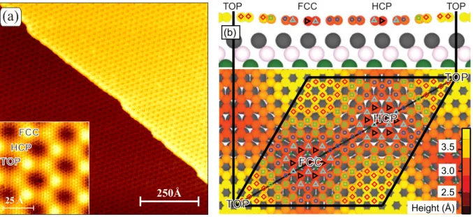
Figure 2.3: (a): STM topographs of Gr/Ir(111). The lattice in the main image is only the moir´ e, while the inset has atomic resolution. Both images show hcp and fcc regions to be apparently higher than top, this is called inverted moir´ e contrast. It is the most common contrast in STM, although other contrasts are also possible depending on the tip and tunneling conditions.
Reproduced from Ref. [54], CC license. (b): Geometry as resulting from a DFT calculation on a (10
×10) on (9
×9) unit cell shows that the hcp and fcc regions are in fact lower than top.
Lower part: Top view, rhombus indicates moir´ e unit cell. Upper part: Side view on a cut plane through the indicated diagonal of the rhombus in the lower part. Color of the carbon atoms encodes their height above the first Ir layer. Reproduced with permission from Ref. [71],
©2012 APS.
point defects. Another major complication of Gr on Ni is the significant solubility of C in Ni at the growth temperatures, which can give rise to precipitation of carbon to the surface to form either multilayer graphene or the surface carbide phase underneath a completed Gr sheet [63], the latter seen in the STM topograph in Fig. 2.2 (e). Thus, graphene on nickel leaves much to be desired in terms of quality, and was used in this thesis in only one project, due to nickel’s ferromagnetism.
In comparison to Ni, the carbon solubility in Ir is small, and no surface carbide phase exists
on the latter’s close-packed surfaces. This is part of a general trend in the interaction strength
of carbon with the metal in the periodic table: It decreases from left to right, and from top
to bottom. Exemplarily for the first row: Ti to Fe form bulk carbides; Co(111) and Ni(111)
still have high carbon solubilities and carbidic overlayer phases on their dense-packed surfaces
competitive with strongly interacting aligned graphene; while for Cu, the carbon solubility is
low [70], and graphene on Cu(111) is weakly interacting.
2.2.4 Atomic structure of graphene on Ir(111)
On Ir(111), rotated graphene phases can form just as in the case of Ni(111) [55]. However, using the TPG+CVD method [72], a single, aligned domain can be easily produced. The TPG (temperature-programmed growth) step refers to the adsorption of ethylene at low temperature, followed by annealing. Graphene flakes covering about 20% of a monolayer form during the heating and form compact islands consisting exclusively of the aligned domain. During the next step, the CVD, these flakes act as seeds for the further growth of fully aligned graphene into a closed film. From now on and throughout the rest of this thesis, Gr/Ir(111) refers exclusively to the aligned domain.
Gr/Ir(111) has an incommensurate superstructure with (10.32
×10.32) graphene unit cells on (9.32
×9.32) Ir unit cells [54]. The moir´ e superstructere is visible in the STM in Fig. 2.3 (a).
Depending on tip and tunneling conditions, it can appear in STM in different contrasts as either high points in a low background, or low points in a high background. The latter is more common, and is referred to as inverted contrast, because it is opposite to the real height of the carbon atoms.
In first-principles calculations, a model with (10
×10) Gr unit cells on (9×9) Ir is the approxi-mation used for the incommensurate cell [56, 71, 73]. Figure 2.3 (b) shows the geometry resulting from a DFT calculation in such a model [71]. Three different regions can be distinguished, ac- cording to whether the center of the carbon ring is located above the hcp, fcc or top sites of the Ir(111) surface [54]. The overall character of the binding is physisorbed, but the smoothly varying relation of the carbon atomic positions with respect to those of the Ir(111) substrate in the moir´ e superstructure results in a chemical modulation of the binding [56]. Gr/Ir(111) has an average height of 3.4 ˚ A, which is similar to what is found in bulk graphite, where the interaction is purely vdW. This contrasts with the height of the most common top-fcc domain of Gr/Ni(111) of about 2.1 ˚ A, which is typical for a chemical bond [67].
In LEED images of Gr/Ir(111) as shown in Fig. 2.4 (a/b), the moir´ e superstructure results in satellite spots around the Gr and Ir ones. In Fig 2.4 (a), we show a SPA-LEED image, which permits to observe the moir´ e also around the zero-order reflection, where an image obtained with a conventional LEED analyzer as shown in Fig. 2.4 (b) is obscured by the electron gun.
One defect that occurs far more often in Gr/Ir(111) than in Gr/Ni(111) are wrinkles [76]. In general for graphene, wrinkles can occur as a result of a transfer process, but this is a different kind of wrinkles compared to the wrinkles in graphene resting on its growth substrate
1. The latter kind of wrinkle results from the negligible thermal expansion of Gr compared to that of the metal substrate. When Gr is grown at high temperature and the sample then cooled down to room temperature, the differential thermal contraction causes a compressive strain in Gr. This strain is partially relieved through the formation of wrinkles, where the Gr locally
1Wrinkles are called ridges in Ref. [55].
2.3. Electronic structure of graphene on Ni(111) and Ir(111)
(b) (c)(a)
Figure 2.4: (a): SPA-LEED image of Gr/Ir(111), intensity in logarithmic scale. Moir´ e satellites appear around the Gr, Ir, and (00) reflexes. Compared to conventional LEED analyzers, SPA- LEED has higher resolution, higher dynamic range, and no electron gun shadow. Reprinted with permission from Ref. [74],
©2012 ACS. (b) Conventional LEED Image (primary electron energy 70 eV) of Gr/Ir(111). Reprinted with permission from Ref. [75],
©2012 AIP. (c): Low-energy electron microscopy (LEEM) image of Gr/Ir(111), field of view 9.3
µm. Thick dark lines areGr wrinkles, thinner wavy lines are Ir steps. Reprinted with permission from Ref. [76],
©2015 Elsevier.
delaminates from the Ir(111) substrate. Figure 2.4 (c) shows a large-scale (9.3
µm) low-energyelectron microscopy (LEEM) image of Gr/Ir(111). The strong dark lines are Gr wrinkles, which form a network. Compared to STM, imaging by LEEM allows a larger field of view, without which the network structure would not be revealed. The wrinkles are preferentially oriented in three different directions, which are the dense-packed rows of the Ir(111) substrate. The crossing point of three wrinkles is often located at a defect [76–78].
2.3 Electronic structure of graphene on Ni(111) and Ir(111)
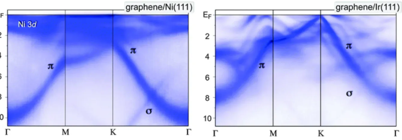
Angle-resolved photoemission spectroscopy (ARPES) can be used to investigate the occupied
part of the electronic band structure of surfaces. Figure 2.5 shows ARPES measurements con-
ducted on (a) Gr/Ni(111) and (b) Gr/Ir(111). For Gr, the most interesting part is the region
around the Dirac point. In Gr/Ni(111), the bands of Gr and the Ni(111) 3d states strongly
hybridize and this destroys the Dirac cone in a wide window around the Fermi edge. In con-
strast, in Gr/Ir(111), the Dirac cone is clearly seen. However, also for Gr/Ir(111), the Dirac
cone is not perfectly preserved: Minigaps and Dirac cone replicas occur as a result of the moir´ e
superstructure [80]; they are not visible in Fig. 2.5 (b), but in Fig. 2.6 (c).
Figure 2.5: ARPES intensity maps of Gr/Ni(111) and Gr/Ir(111) on a line through the Γ- M-K-Γ high-symmetry points of the Brillouin zone. Reprinted with permission from Ref. [79],
©
2012 RSC.
2.4 Intercalation of graphene on metals
It is energetically favorable for many species deposited onto graphene to intercalate in between graphene and the substrate, because the bond of the species to the substrate is stronger than the bond of graphene to the substrate, due to graphene’s low reactivity. The intercalation of graphene is useful to modify graphene’s properties and its interaction with the support, without changing the growth substrate and without any mechanical transfer process. For the purposes of this thesis, there are the following four applications of intercalation:
The first application is to dope graphene with electrons or holes. Doping by intercalation permits large shifts of the Fermi level on the order of
±1 V [81]. The doping of graphene resultsin a shift of the Dirac cone up and down relative to the Fermi level. This is directly visible in ARPES measurements: In Gr/Ir(111), the Dirac point is located very close to the Fermi level as seen in Fig. 2.6 (a) and (c). In contrast, the ARPES measurements shown in Fig. 2.6 after intercalation of (b) Cs and (d) O show that the Dirac point is shifted down (Cs) or up (O) due to
nand
pdoping by about
−1.1 eV and +0.6 eV, respectively.The second application of intercalation is to “decouple” graphene from its support, where
decoupling can have different meanings: It either means that (1) the electronic features of
freestanding graphene, in particular a well-developed Dirac cone, are recovered, or (2) that the
binding to the support is weakened, including the binding at the edges of graphene flakes, where
the dangling
σbonds might bind to the substrate. Electronic decoupling of Gr/Ir(111) has
been obtained by intercalation of O, Eu, Cs, Au, Ag. This, too, is well visible in the ARPES
in Figure 2.6 (b) and (d), where the minigaps and Dirac cone replicas of Fig. 2.6 (a) and (c)
have disappeared in both cases. Evidence for structural decoupling of Gr/Ir(111) is available
for intercalation of Br [82] and Au [65], but is not relevant for this thesis.
2.4. Intercalation of graphene on metals
–3.0 –2.5 –2.0 –1.5 –1.0 –0.5 0.0
E−EF(eV)
–0.2 0.0 0.2 –0.2 0.0 0.2
b
–0.2 0.0 0.2
c a
0.2 –0.2 0.0 0.2
b
–0.2 0.0 0.2
c b
c d
Figure 2.6: (a), (c): ARPES intensity maps of Gr/Ir(111) around the K point show the Dirac cone with minigaps at around -0.7 eV. (b), (d): After intercalation of one monolayer of Cs and O, respectively.
ndoping by Cs shifts the Dirac cone down relative to the Fermi level, while
pdoping by O shifts it up. Both Cs and O decouple Gr as seen in the disappearance of the minigaps. (a,b): Reproduced from Ref. [78], open access. (c,d): Reprinted with permission from Ref. [7],
©2012 ACS.
(a) (b) (c) (d)
Figure 2.7: (a)–(d) STM topographs [image size (80 nm)
2] after intercalation of Eu resulting in successively larger intercalation coverages of (a) 18% ML, (b) 39% ML, (c) 72% ML, and (d) 89% ML. Reprinted with permission from Ref. [83],
©2013 APS.
The third application of intercalation is to bring graphene into contact with a magnetic material. While graphene can be grown directly on some ferromagnetic metals as described before, the growth of Gr on Ir(111) followed by intercalation can result in very different kinds of Gr-substrate interfaces. Gr/Ir(111) intercalated with monolayer thin layers of Fe, Ni, and Co has been investigated by several researchers, who found peculiar spin textures, modified magnetic remanence, and a small induced magnetization in Gr [8, 18, 84, 85].
The fourth application is to pattern graphene in a self-organized way on a length scale of
nanometer. As shown in Fig. 2.7, the intercalation of submonolayer amounts of Eu gives rise
to a pattern consisting of Eu stripes, Eu islands, and Eu-free channels [83]. The pattern results
3 4 5 6 7 8
−1
−0.8
−0.6
−0.4
−0.2 0 0.2 0.4
separation [Å]
Energy [eV]
temperature [K]
desorption rate
(c)
(d)
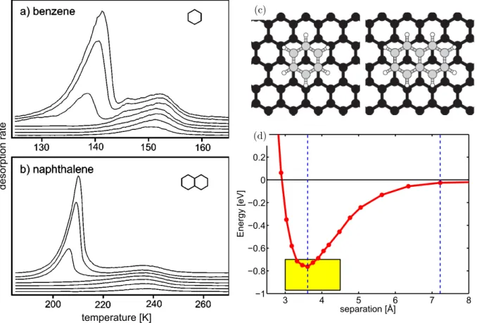
Figure 2.8: (a) and (b): Thermal desorption spectra for benzene and naphthalene from graphite for several coverages, heating rate 0.7 K/s and 1.0 K/s, respectively. Curves vertically offset for clarity. Reprinted with permission from Ref. [87]
©2004 APS. (c): Adsorption geometry of benzene and naphthalene on Gr as predicted by vdW-DFT. (d): Energy vs. adsorption height for naphthalene on Gr as calculated in vdW-DFT, yellow box gives the range of experimental values of the binding energy. (c) and (d) are reprinted with permission from Ref. [88],
©2006 APS.
from the slight inhomogeneity of the binding of Gr/Ir(111) in different moir´ e regions, coupled to the compressive strain in graphene due to the differential thermal expansion. The Gr is locally
ndoped in the Eu-intercalated regions, but only hardly doped in the non-intercalated regions [86].
2.5 Adsorption of benzene and naphthalene on graphite
As a model case of
π-πinteraction, the adsorption of benzene and naphthalene on graphite has been studied by several authors using LEED [89, 90], TDS [87], DFT [88], and STM [91].
In LEED, both benzene and naphthalene form well-ordered superstructures also at submono-
layer coverages, implying an attractive interaction of the molecules, although the behavior for
naphthalene is rather complex [90]. Also for both molecules, the superstructures in LEED dis-
appear and reappear reversibly upon heating and cooling through a critical temperature. This
suggests that the molecular islands melt before desorption and the molecules thus desorb from a
2.6. Organometallic sandwich complexes and nanowires fluid on-surface phase, such that the influence of the intermolecular interaction on the desorption process is rather weak.
In thermal desorption experiments as shown in Fig. 2.8 (a) and (b), the desorption kinetics are first order for both benzene and naphthalene, although the transition between monolayer and multilayer behavior is more complex for benzene. First-order kinetics are expected for individually desorbing molecules, in line with the results from LEED.
In DFT calculations, the adsorption geometry of the molecules is found to be as shown in Fig. 2.8 (c). It is analogous to the stacking of graphene layers in graphite. Inclusion of the vdW interaction via the Langreth-Lundqvist vdW-DF method [92] yields a curve for energy vs.
separation as shown in Fig. 2.8 (d), here exemplarily only for naphthalene. The benzene curve is the same except for the different energy scale. The curve implies that the barrier for the desorption process is identical to the binding energy of the molecule. By calculations using the vdW-DF method, a binding energy in good agreement with the experimental value is found.
2.6 Organometallic sandwich complexes and nanowires
The prototypical organometallic sandwich compound is ferrocene, and the discovery of its struc- ture was a milestone of organometallic chemistry [93]. It consists of one Fe atom sandwiched between two cyclopentadienyl (Cp) rings (C
5H
5=Cp). Fischer and Wilkinson suggested fer- rocene’s structure and were awarded the 1973 Nobel prize in chemistry “for their pioneering work performed independently on the chemistry of the organometallic, so-called sandwich com- pounds.”
The neutral cyclopentadienyl C
5H
5is a radical, because the total number of valence electrons (5
·4 + 5·1 = 25) is odd. However, adding one electron from a ligand, an aromatic configuration can be obtained: Each of the C atoms contributes one electron to the
πsystem, and one from the ligand to yield 6 in total, which satisfies the H¨ uckel rule for aromaticity (π electron number of the form 2 + 4n). Thus, Cp acts as an anion.
For ferrocene, the high stability also rests on the number of 18 valence electrons: 5 each from the
πsystems of the two Cp rings, and 8 from the Fe atom. The number 18 is magic because it is of the form 2n
2, just like the atomic numbers of the noble gas atoms. The number of 18 valence electrons can also be obtained by combining Cr with two benzene (Bz) rings, and the compound CrBz
2is also very stable. In these compounds, Cr and Bz are both formally zerovalent. Substituting Cr with V yields VBz
2, a 17 electron system, which is paramagnetic with one unpaired spin [94].
It is natural to expand on the idea of sandwich compounds by alternately stacking more metal
atoms and aromatic rings on top of each other. This gives a multidecker sandwich compound, and
in the limiting case an organometallic sandwich molecular wire (SMW), or simply nanowire. An
alkali metal can donate one electron to one Cp ring, and compounds such as CsCp indeed form
(a) (b)
(c)
Figure 2.9: (a): Time-of-flight mass spectrum of the gas-phase reaction of V with Bz, peaks are labeled with (n,m) according to V
nBz
m. (b): Model of multidecker full-sandwich structures.
(c): Model of riceball structures formed for 3d metals heavier than Cr. All subfigures reproduced with permission from Ref. [96] ACS 1999.
bulk crystals with a structure made of parallel SMWs [95]. However, no interesting electronic magnetic properties are expected in CsCp. In contrast, the VBz SMW has been predicted to be a ferromagnetic half-metal, i.e., metallic for one spin direction, and semiconducting for the other [37].
Some SMWs can be produced by synthesis in solution [95, 97], however, a larger number has been produced by the gas-phase reaction of laser-evaporated metal atoms with the ligands in a noble gas stream, chiefly by the group of Nakajima [96]. The complexes could be characterized by time-of-flight mass spectrometry for composition, photoemission spectroscopy for electronic structure, and Stern-Gerlach method (beam deflection by an inhomogeneous magnetic field) for the magnetic moments.
Figure 2.9 (a) shows a mass spectrum obtained from the reaction of the V with Bz. The strongest peaks are at the masses corresponding to complexes with composition V
nBz
mwith
m=
n+ 1, which are called full-sandwich complexes due to their termination by a Bz molecule on both sides as shown in Fig. 2.9 (b). The sandwich structure with Bz is preferred only for the lighter 3d metals, up to Cr, while the heavier 3d prefer to form so-called “riceball” structures as depicted in Fig. 2.9 (c), where a cluster of metal atoms is surrounded by Bz molecules [96].
In contrast to Cp, which requires one additional electron to become aromatic, and Bz, which
requires none, the compound cyclooctatetraene (Cot = C
8H
8) requires two additional electrons
to fulfill the H¨ uckel rule with 10 electrons. Therefore, Cot can form SMWs with sufficiently
electropositive, divalent metals. The rare-earth metals are magnetically interesting and give
away their 6s
2electrons easily. While they are mostly trivalent, some of them occur divalent
as well. Among the magnetically interesting divalent rare-earth ions, Eu
2+is by far the most
stable, due to the half-filled 4f shell and the resulting maximum stabilization from Hund’s rule
energy of the parallel electron spins. The EuCot SMW was predicted to be a ferromagnetic
semiconductor.
2.6. Organometallic sandwich complexes and nanowires
(a)(b)
(c) (d)
Figure 2.10: (a), (b): Time-of-flight mass spectra of products of the reaction of Cot with Eu and Tm, respectively. Peaks are labeled (m,n) corresponding to (Eu, Tm)
n, Cot
m. (c), (d):
Model of the oxidation states for (c) most lanthanides (d) Eu and Yb. (a), (b): Reproduced with permission from Ref. [98],
©ACS 2008. (c), (d): Reproduced with permission Ref. [96] ACS 1999.
Figure 2.10 (a) and (b) show mass spectra resulting from the reaction of Cot with Eu and Tm, respectively (the choice of Tm is motivated in section 7.3). As in the case of VBz, the main peaks can be indexed with
n=
m±1. However, additional peaks in between resulted in this experiment, because the low reaction temperature facilitated the attachment of weakly-bound, physisorbed molecules on the wires. Furthermore obvious from the comparison of Fig. 2.10 (a, b) with Fig. 2.9 (a) is the higher intensity for longer wires in the former, up to
n= 10 in this measurement, and beyond
n= 20 elsewhere for EuCot [99].
Figure 2.10 (c) and (d) show a model of the oxidation states of the lanthanides in finite- length wires with Cot. The model has been developed based on photoemission spectroscopy, experiments with attachment of Na atoms, and electron affinities. Inside a wire, there is one Cot ring for every Ln atom, such that the oxidation state is 2+. However, at a Cot-terminated wire end, most lanthanides will be oxidized to the 3+ oxidation state, so that Cot can assume its favorable
−2 state also at the wire end. Only the lanthanides Eu and Yb, which have aparticularly stable 4f electron configuration, which is half-full and full, respectively, do not give an oxidation state higher than +2 in reaction with Cot.
Stern-Gerlach-type experiments yield magnetic moments of VBz [100] and EuCot [98] which
scale linearly with the number of metal atoms in the complex, while for TmCot, the suppression
of magnetic moments in larger clusters was suggested to be the result of antiferromagnetic
interactions [98].
Chapter 3
Experimental methods
The experimental methods used in this thesis are scanning tunneling microscopy (STM), low- energy electron diffraction (LEED), thermal desorption spectroscopy (TDS), x-ray absorption spectroscopy (XAS), and x-ray magnetic circular dichroism (XMCD).
3.1 Scanning tunneling microscopy
Scanning tunneling microscopy is capable of resolving atoms, and the STM’s developers Gerd Binnig and Heinrich Rohrer were awarded the 1986 Nobel Prize for the development of this instrument, the prize being shared with Ernst Ruska, the developer of the electron microscope, another technique that has advanced to atomic resolution. Since then, STM has become ubiq- uitous and has been reviewed often, see for example Ref. [101].
In an STM, an electrically conducting sample surface is imaged by a conducting tip, making
use of the quantum mechanical tunneling of electrons through a vacuum gap between tip and
sample. A bias voltage
Uis applied to obtain a net current. When the tip is held at a distance
of about 1 nm above the surface, the tunneling effect leads to a current
Ithat is exponentially
dependent on the distance
dbetween tip and sample. As the height of the tunneling barrier is
given by the work functions of tip and sample, the decay length into the barrier is on the order
of the wavelength of electrons with that kinetic energy. Typically, a change of the tip-sample
separation 1 ˚ A leads to an order of magnitude difference in the conductivity, giving STM a high
vertical sensitivity. The height of the tip (Z ) and its lateral position (X,
Y) over the sample can
be controlled on the sub-˚ A scale using piezo elements. In the most commonly employed constant-
current mode, a feedback loop regulates the voltage on the
Zpiezo to minimize the deviation
between the measured tunneling current and a current setpoint, the latter controlled by the
operator. The setpoint current is typically in the range of pA to nA. The lateral position (X,
Y) is scanned line-by-line while the feedback loop output
Zis recorded to obtain a topographic
image.
STM is generally not sensitive to the positions of the atomic nuclei, but rather to the local density of states in the energy interval between the Fermi level and the applied bias voltage.
Furthermore, it is just as sensitive to the properties of the tip as it is to those of the surface.
Mathematically, this is expressed as the tunneling current resulting from the convolution of the space- and energy-dependent density of states of the tip
ρTand that of the sample
ρSaccording to
I ∼ Z +∞
−∞
|M|2
[f (E
−eU)−f(E)]ρS(E
f −eU)ρT(E
f)
where
Mis the tunneling matrix element,
f(E) is the Fermi function describing the occupation of levels at a finite temperature, and
ethe elementary charge.
Because STM probes the local density of states many ˚ A away from the atoms, the observed weight of the electronic states can differ rather strongly from that inside the material, as elec- tronic states vary in their asymptotic decay towards the vacuum. For example, states with high parallel momentum, such as those at the K points of graphene, decay faster than those near the Γ point [102], and their rapid decay often makes localized 4f states inaccessible to STM [103].
3.2 Low-energy electron diffraction
Low-energy electron diffraction (LEED) from a surface was the first proof of the wave nature of electrons [104]. A recent introduction to the LEED technique in surface science is given in Ref. [105].
In a nowadays typical rear-view hemispherical LEED analyzer, a beam of monochromatic low-energy electrons (tunable, typically
E= 10 up to 1000 V) impinges on the sample surface, almost always in or close to normal incidence. Because of the small penetration depth of elec- trons of the order of a few ˚ A (also depending on the energy), the method is highly surface sensitive. From the backscattered electrons, only the elastically scattered part is filtered out by a hemispherical retarding grid. The electrons are converted into visible light by acceleration with a high voltage of typically around 5 kV onto a fluorescent screen. Crystalline order in the sample plane leads to a diffraction pattern on the screen.
At the surface, the translational symmetry normal to the surface is always broken, and therefore, the electron momentum in this direction is not preserved. This relaxes the Laue con- dition from the three-dimensional case, and as a result, diffracted beams have non-vanishing intensity at almost all energies also on a single-crystal surface. This contrasts to x-ray diffrac- tion, where a monochromatic x-ray beam impinging on a single crystal almost always does not give diffracted beams, and either polychromatic x-rays (Laue method), polycrystalline samples (Debye-Scherrer method), or four-circle instruments (to also control the orientation of the crystal axes with respect to the beam) are employed.
For a normally incident primary electron beam, the zero-order diffracted beam is reflected
3.3. Thermal desorption spectroscopy back into the electron gun, which is mounted in the center of the screen. The other diffracted beams move toward the center of the screen with increasing energy as the electron wavelength becomes shorter and the diffraction angles smaller.
In a conventional LEED instrument, the primary electron beam current is typically of the order of a few
µA. This current is sufficient to damage sensitive structures on the sample, suchas weakly bound adsorbates or molecular systems. In such cases, microchannel plate (MCP) LEED instruments should be used, which feature either a single MCP or a chevron double MCP between the retarding grid and the screen to amplify the diffracted beams. This allows to reduce the primary beam current, down to a few nA for single MCP, and to below 100 pA with a double MCP. Because the MCPs can only be manufactured as flat discs, and not as hemispheres, the diffraction pattern in such instruments is geometrically distorted.
3.3 Thermal desorption spectroscopy
Thermal desorption spectroscopy is a very common method in surface science [106], and is also called temperature-programmed desorption. Typically, a sample surface with a coverage
θof adsorbates is heated at a constant ramp rate
β, while a mass spectrometer above the surfacemeasures the intensity at the mass of the adsorbate. The desorption process is described by the Wigner-Polanyi equation
−dθ
dt
=
θnνe−kB TEA(3.1)
with
nthe order of the desorption process,
νthe attempt frequency, and
EAthe activation energy, which is equal to the binding energy for non-activated adsorption. The attempt frequency
νis of the order of the phonon frequency in simple cases. Note that
Tvaries with time as it is ramped. Furthermore,
νand
EAmay change with the coverage.
The order of the desorption process
ncan take various values: In case of the desorption of a thick film, the behavior is like the evaporation of a bulk sample, and it is always
n= 0, the Wigner-Polanyi equation being equivalent to an equation for the vapor pressure. In the case of a monolayer or less of non-interacting adsorbates, which desorb individually and independently from one another, it is
n= 1. For adsorbates that exist on the surface as monomers but have to desorb as dimers, e.g., chemisorbed oxygen atoms desorbing as O
2molecules, it is
n= 2.
And when the rate-limiting step is the desorption of molecules from the one-dimensional edge of two-dimensional islands existing on the surface, it is
n=
12.
The equation 3.1 is a differential equation without closed form solutions for most
n. For n= 1, the temperature
Tmaxwhere the desorption rate peaks can be approximated with the Redhead formula:
EA
=
kBTmax
ln
νTmax
β
−
3.64
(3.2)
3.4 X-ray absorption spectroscopy
The advent of intense, tunable, and polarized synchrotron-based x-ray sources has created en- tirely new experimental methods and corresponding fields of research in the last decades. In x-ray absorption spectroscopy (XAS), one looks at optically excited transitions of electrons from a core-shell into the unoccupied valence states. In a simple one-electron picture, the core state is a source of photoelectrons, which are then used to probe the valence states. Dipole-allowed transitions are the strongest and thus most commonly investigated, i.e., the difference in the angular momentum quantum number of the core and valence shell is ∆L =
±1.To measure the absorption, various modes are employed, such as transmission, fluorescence yield, or total electron yield (TEY). In this thesis, TEY is used exclusively, due to its high surface sensitivity. In the soft x-ray region, the decay of the core-level photo-hole proceeds predominantly via an Auger process, which leads to emission of electrons from the sample surface into the vacuum, both directly, and via generation of secondary electrons. The charge lost from the sample reaches ground via the metallic inner walls of the experimental apparatus.
The sample is virtually grounded via a current amplifier, and the measured current is the signal.
The method is surface sensitive because the escape path length of electrons up to the keV range is typically in the nanometer range. The penetration depth of the x-rays must be large compared to the electron escape depth, or otherwise, a saturation behavior is observed, which distorts the peak shape and leads to errors in the analysis [107, 108].
The processes dominating the line shapes in XAS are very different depending on the elements and transitions considered: In the 1s to 2p transition (K edge) of graphite, the line shape can be related to the density of states of the
p-derived valence bands and their symmetry [109]. Incontrast, in the 2p to 3d transitions of the first-row transition metals, the interaction of the core hole with the valence electrons additionally leads to a so-called multiplet structure, which is however generally still convoluted with the density of states in the valence band. The multiplet structure in the 2p to 3d transitions is thus less apparent in metallic films and becomes clearest for single 3d atoms [110]. In contrast in the rare-earth elements, because of the small bandwidth of the 4f level, the 3d to 4f spectral shape is generally dominated by the multiplet structure.
There, the line shape depends almost exclusively on the number of 4f electrons in the ground state.
3.5 X-ray magnetic dichroism
Magnetic dichroism is the difference in optical properties, such as absorption, for differently
polarized light in magnetic samples. Circular magnetic dichroism occurs for circularly-polarized
light between helicities parallel and antiparallel to the magnetization, while magnetic linear
dichroism occurs for linearly-polarized light between polarizations parallel and perpendicular to
3.5. X-ray magnetic dichroism
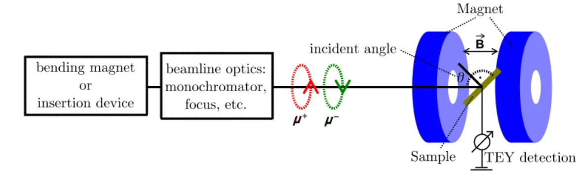
Magnetθ
Sample
incident angle B
μμ μμ beamline optics:
monochromator, focus, etc.
bending magnet or insertion device
TEY detection
Figure 3.1: Sketch of the experimental setup for the XMCD measurement. Partially adapted from Ref. [111],
©2014 Elsevier.
magnetization. The unique capability of x-ray dichroism compared to other methods of magnetic characterization are (1) the elemental sensitivity, which arises from the characteristic core levels for every element, and (2) the ability to assess spin- and orbital moment separately. Note that in this section, we review only circular dichroism, as the linear one was strong in only one element (Tm) investigated in this thesis, and is thus discussed in the corresponding section 7.6.
The most commonly investigated elements are those of the 3d and 4f series. There, the dipole-allowed transitions are 2p to 3d for the 3d transition metals and 3d to 4f for the rare- earth metals. Due to spin-orbit coupling, the core level is split into 2p
3/2, 2p
1/2and 3d
5/2, 3d
3/2, respectively. The spin-orbit interaction is so strong that the lines are generally well separated in energy. The absorption edges resulting from the 2p
3/2and 2p
1/2level are also referred to as
L3and
L2, while those from the 3d
5/2and 3d
3/2are also referred to as
M5and
M4. These edges lie in the soft x-ray range: In the 3d elements, the
L3,2start at 399 eV (for Sc) and go up to 950 eV (for Cu), while in the 4f elements, the
M5,4start at 836 eV (for La) and go up to 1576 eV (for Yb). The absorption cross-sections are high enough that a sensitivity down to 1 % of a monolayer can be obtained with TEY. In this thesis, only soft x-rays were used; hard x-rays require different measurement setups, but permit other elements, e.g., at the
L3,2edge of Pt (around 12 keV) in FePt
L10[112].
3.5.1 X-ray magnetic circular dichroism
There are a number of reviews on x-ray magnetic circular dichroism (XMCD) [111, 114–116].
A typical measurement setup for XMCD measurements is shown in Fig. 3.1. The circularly- polarized, monochromatic x-ray beam impinges on the sample under an incident angle
θto the surface normal. Varying
θallows access to the magnetic anisotropy. The sample is located in a magnet, where the magnetic field is always parallel or antiparallel to the incoming light.
Explaining the XMCD effect is simplest in the so-called two-step model, which is sketched
for the 3d transition metal case in Fig. 3.2 (a). The first step is the excitation of an electron
from the core level. Because of the spin-orbit coupling in the core level, the excited electrons
have a partial spin polarization, which depends on the helicity of the incoming light: From
(a) H M≠0 H M≠0
2p3/2 2p1/2 EF
Energy
L2 L3
37.5%
25% 75%
62.5%
L2 L3
μμ μμ
2p3/2 2p1/2 EF
Energy
L2 L3
62.5%
75% 25%
37.5%
L2 L3
Figure 3.2: (a) Diagram of the two-step picture of XMCD, explanation see text. Reprinted with permission from Ref. [111],
©2014 Elsevier. (b) XAS at the Fe L
2,3for right (µ
+) and left (µ
−) circular polarization. (c) Difference spectrum, the XMCD (solid line) and integrated XMCD (dotted line) to obtain
pand
q. (d) Polarization-averaged XAS with double step backgroundand integral
r. (b) to (d) reprinted with permission from Chen et al. [113], ©1995 APS.
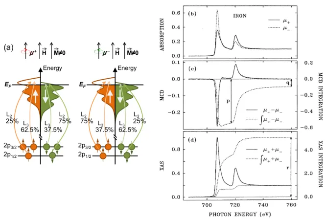
the 2p
3/2level (L
3edge), x-rays with positive helicity excite 62.5% spin up electrons and those with negative helicity excite 37.5% spin-up electrons, while from the 2p
1/2level (L
2edge), these numbers are 25% and 75%, respectively. The second step is then for this excited electron to find a hole in the magnetic 3d valence shell. If the valence shell carries a spin- or orbital moment, there will be an imbalance in the number of holes for the different spin and orbital moment directions, and the absorption cross-section will change with the magnetization.
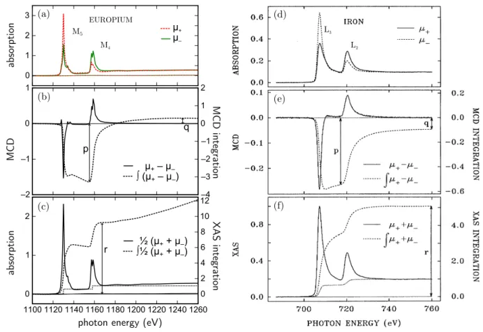
In Fig. 3.2 (b) to (d), a typical XMCD measurement is shown as obtained at the L
3,2edges of a film of metallic Fe. The absorption spectra
µ+,
µ−are acquired for opposite helicities of the incoming light (or, equivalently, opposite magnetization directions). The XMCD is then calculated as the difference spectrum,
µXM CD
=
µ+−µ−(3.3)
and exhibits opposite sign at the L
3and L
2edges due to the opposite predominant spin polar-
ization of the photoelectrons excited from the two corelevels.
3.5. X-ray magnetic dichroism 3.5.2 XMCD sum rules
This subsection reproduces material from the master thesis of S. Kraus [117].
The XMCD sum rules developed by Thole et al. [118] and Carra et al. [119] relate the integrated intensities at the two spin-orbit split edges to the expectation values of the spin and orbital moment.
We define the polarization-averaged XAS spectrum as
µaverage= 1
3 (µ
++
µ−+
µ0) (3.4)
where
µ0is the isotropic spectrum.
µ0is not commonly measured and so one usually takes instead
µ0
= 1
2 (µ
++
µ−) (3.5)
although this is only valid when linear magnetic dichroism is negligible. For analysis, the areas under the different edges have to be evaluated. We define the integral over the first absorption edge of the XMCD spectrum as
p
=
Zj+
dE
(µ
+−µ−), (3.6)
the integral over both edges of the XMCD spectrum as
q=
Z
j++j−
dE
(µ
+−µ−) (3.7)
and the integral over both edges of the averaged XAS spectrum as
r=
Z
j++j−
dE
1
3 (µ
++
µ−+
µ0). (3.8)
For the 3d and 4f elements,
j+/−correspond to L
3/2and M
5/4, respectively.
In Ref. [119], Carra et al. give the sum rules in the most general case. To avoid confusion every symbol used in the formulas is listed in Table 3.1.
The expectation value of the orbital momentum operator satisfies eq. 3.9.
q
3r = 1
2
l(l
+ 1) + 2
−c(c+ 1)
l(l
+ 1)(4l + 2
−n) · hLzi(3.9)
The expectation values of the spin and magnetic dipole operator satisfy eq. 3.10.
p−(c+ 1)/c(q−p)
3r = l(l+ 1) + 2−c(c+ 1)
3c(4l+ 2−n)) · hSzi +. . .
· · ·+ l(l+ 1)[l(l+ 1) + 2c(c+ 1) + 4]−3(c−1)2(c+ 2)2 6lc(l+ 1)(4l+ 2−n) · hTzi
(3.10)