Magnetic quantum ratchet effect in (Cd,Mn)Te- and CdTe-based quantum well structures with a lateral asymmetric superlattice
P. Faltermeier,1G. V. Budkin,2J. Unverzagt,1S. Hubmann,1A. Pfaller,1V. V. Bel’kov,2L. E. Golub,2E. L. Ivchenko,2 Z. Adamus,3G. Karczewski,3T. Wojtowicz,3,4V. V. Popov,5,6D. V. Fateev,5D. A. Kozlov,7D. Weiss,1and S. D. Ganichev1
1Terahertz Center, University of Regensburg, 93040 Regensburg, Germany
2Ioffe Institute, 194021 St. Petersburg, Russia
3Institute of Physics, Polish Academy of Sciences, al. Lotników 32/46, PL 02-668 Warszawa, Poland
4International Research Centre MagTop, al. Lotników 32/46, PL 02-668 Warszawa, Poland
5Institute of Radio Engineering and Electronics (Saratov Branch), 410019 Saratov, Russia
6Physics Department, Saratov State University, 410012 Saratov, Russia
7A.V. Rzhanov Institute of Semiconductor Physics, 630090 Novosibirsk, Russia (Received 9 February 2017; published 24 April 2017)
We report on the observation of magnetic quantum ratchet effect in (Cd,Mn)Te- and CdTe-based quantum well structures with an asymmetric lateral dual grating gate superlattice subjected to an external magnetic field applied normal to the quantum well plane. A dc electric current excited by cw terahertz laser radiation shows 1/B oscillations with an amplitude much larger as compared to the photocurrent at zero magnetic field. We show that the photocurrent is caused by the combined action of a spatially periodic in-plane potential and the spatially modulated radiation due to the near-field effects of light diffraction. Magnitude and direction of the photocurrent are determined by the degree of the lateral asymmetry controlled by the variation of voltages applied to the individual gates. The observed magneto-oscillations with enhanced photocurrent amplitude result from Landau quantization and, for (Cd,Mn)Te at low temperatures, from the exchange enhanced Zeeman splitting in diluted magnetic heterostructures. Theoretical analysis, considering the magnetic quantum ratchet effect in the framework of semiclassical approach, describes quite well the experimental results.
DOI:10.1103/PhysRevB.95.155442
I. INTRODUCTION
Spatially periodic noncentrosymmetric systems are able to transport nonequilibrium particles in the absence of an average macroscopic force resulting in the ratchet effect [1–5]. Ratchet effects whose prerequisites are simultaneous breaking of both thermal equilibrium and spatial inversion symmetry can be realized in a great variety of forms and, in particular, as electric transport in semiconductor systems [6–20]. Recent experiments demonstrated that terahertz radiation induced ratchet effects can be efficiently excited in semiconductor quantum wells (QWs) [14,15,21,22] and graphene [23,24]
with lateral superlattice structures. These experiments al- lowed one to explore basic physics of the ratchet effects in low dimensional electron systems, provide information on nonequilibrium transport in such systems, and demonstrate that ratchet effects can be applied for room temperature terahertz radiation detection [25–28]. The latter, besides high sensitivity and short response times, offer new functionality being a good candidate for all-electric detection of the radiation polarization state including radiation helicity [29–32].
Here we report on the observation and study of magnetic quantum ratchet effect in (Cd,Mn)Te/(Cd,Mg)Te diluted mag- netic heterostructures and CdTe/CdMgTe QWs superimposed with lateral asymmetric superlattices. Applying magnetic field B along the growth direction we observe that the ratchet current exhibits sign-alternating 1/B-periodic oscillations with amplitudes immensely larger than the ratchet signal at zero magnetic field. The results are analyzed in terms of the theory of magnetic ratchet effects in QW structures with a lateral asymmetric periodic potential [33]. We show that the photocurrent generation is based on the combined action
of a spatially periodic in-plane potential and the spatially modulated light due to the near-field effects of radiation diffraction. Corresponding theoretical analysis describes the experimental results.
The paper is organized as follows. First, we present our samples and results of magnetotransport characterization (Sec.II), as well as briefly describe the experimental technique (Sec.III). In Sec.IVwe discuss the results on the photocurrents generated at zero magnetic field. SectionVcontains the main experimental results on the magnetic quantum ratchet effect.
It has three subsections describing the basic results, the laser beam scan across the structure, and the effect of the electro- static potential acting on the electron gas. In the following Sec.VIwe present the theory, calculate dependencies of the photocurrent on magnetic field, and compare them with the experimental data. Finally, in Sec. VII we summarize the results and discuss prospectives of future experimental studies of the magnetic quantum ratchet effect.
II. SAMPLES
A. Samples grow and characterization
Experiments are carried out on (Cd,Mn)Te/CdMgTe and CdTe/CdMgTe single QW structures grown by molecular beam epitaxy on (001)-oriented GaAs substrates [34–38].
During the growth the fluxes of Cd, Te, Mg, and Mn have been supplied from elemental sources while iodine flux has been obtained from a ZnI2 source. The schematic layout of the (Cd,Mn)Te/CdMgTe layer structure and sketch of the QW are presented in Fig.1. The thick buffer (≈6μm), consisting of CdTe and Cd0.76Mg0.24Te layers and CdTe/Cd0.76Mg0.24Te
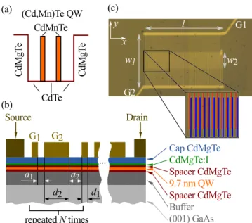
FIG. 1. (a) Sketch of CdMgTe/(Cd,Mn)Te/CdMgTe QW. Two red bars show evenly spaced 3 monolayer thick Cd0.8Mn0.2Te layers inserted during QW growth. (b) Cross section of the dual-grating gate superlattice formed by metal fingers deposited on top of the QW structure. Structure composition is given on the right side of the sketch. The supercell of the grating gate fingers consists of metal stripes having two different widthsd1 andd2separated by spacings a1anda2. This asymmetric supercell is repeatedN times to create a superlattice with period d=d1+a1+d2+a2, see Table I. (c) Photograph of the sample together with schematic top view of the dual-grating gate superlattice. Thin red and thick blue lines sketch the top gates having different thicknesses and spacings.
short period superlattices, have been grown to reduce the number of dislocations resulting from the strong lattice mismatch between GaAs and Cd1−xMgxTe. The well width in both kinds of structures is 9.7 nm and the Cd0.76Mg0.24Te alloy serves as a barrier material. The composition of barriers has been determined from photoluminescence spectra. In order to obtain a two-dimensional electron gas the structures have been modulation doped by iodine donors incorporated into the 5-nm-thick region of the top barrier at the distance of either 10 or 15 nm away from the QW, in (Cd,Mn)Te/CdMgTe and CdTe/CdMgTe structures, respectively. Doped regions have been overgrown by an undoped cap layer with thickness of either 50 nm, for (Cd,Mn)Te/CdMgTe QWs, or 75 nm, for CdTe/CdMgTe QWs. The density of the two-dimensional electron gasneand the electron mobilityμdetermined at liquid helium temperature (4.2 K) for (Cd,Mn)Te/CdMgTe structures are ne=6.6×1011 cm−2 andμ=9.5×103 cm2/V s, and for CdTe/CdMgTe structuresne=4.2×1011cm−2andμ= 65×103cm2/V s.
(Cd,Mn)Te/CdMgTe structures contain a single QW made of (Cd,Mn)Te digital magnetic alloy [39], while CdTe/CdMgTe structures contain a single QW made of nonmagnetic CdTe. In the former structures two evenly spaced Cd0.8Mn0.2Te thin layers were inserted during the QW growth, see Fig.1(a). These two layers were 3 monolayer thick (ML) and separated from each other and from the barriers by 8 ML thick CdTe (1 ML is 0.324 nm thick).
UG1/G2(V) -1 -0.6
R xx
(k Ω )7.2
6.8
B =3.9 T UG1=0 UG2=0
R xx
(k Ω )
6 9 12
0 1 2 3 4 5 6 7 B (T)
1
0 2 3
0 1 2 3 4 5 6 7 B (T)
Sample #1 T = 4.2 K B (T)
2 6
R xy
(kΩ)
) b ( )
a (
0 2 6
Hallbar sample T = 1.6 K
4
R xx
(k Ω )
y B x
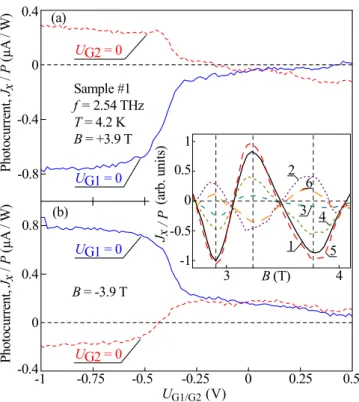
FIG. 2. Magnetotransport experiments performed at tempera- turesT =1.6 and 4.2 K in (Cd,Mn)Te structures. (a) Unpatterned Hall bar sample. (b) Square shaped samples with a DGG superlattice.
For this measurement a van der Pauw geometry has been used.
Inset in (b) shows the dependence of the longitudinal resistanceRxx
on the gate voltage UG1 (UG2) measured forUG2=0 (UG1=0).
Measurements are presented for B=3.9 T corresponding to a maximum of theRxx oscillations. Bottom inset in (b) sketches the DGG sample.
Incorporation of Mn2+ ions carrying localized spinS = 5/2 into the QW region leads to a strong enhancement of the effective g factor of band carriers, and hence to an enhanced Zeeman splitting. This has been shown in previous magnetophotoluminescence (PL) studies performed on the (Cd,Mn)Te/CdMgTe samples made from the same wafer as used in the current study. Magneto-PL showed strong redshift of the PL line with increasing magnetic field [37]. From fitting of the modified Brillouin function [40,41] to the field dependence of the PL line position the effective average concentration of Mn in the digital alloy has been estimated to be ¯x=0.015. The samples have also been characterized by electrical transport measurements. At low temperatures pronounced Shubnikov–de Haas (SdH) oscillations and very well resolved quantum Hall plateaus have been observed.
Two characteristic dependencies measured in Hall bar and van der Pauw geometries in (Cd,Mn)Te structures are shown in Figs.2(a) and2(b), respectively. While the amplitude of the oscillations increases in CdTe and (Cd,Mn)Te structures at rather high temperatures with raising magnetic field, the amplitude of the oscillations in (Cd,Mn)Te at low temperatures is a more complex function of the magnetic field B and shows a beating like pattern. The latter is clearly seen in Fig. 2(a) for T =1.6 K (B >3.5 T) and in Fig. 2(b) for 4.2 K (B >4.5 T). Such a behavior in diluted magnetic semiconductor (DMS) structures is well known to be caused by the exchange interaction of electrons with Mn2+ions resulting in the exchange-enhanced Zeeman splitting [39,41–43].
B. Dual grating top gate structure
For the ratchet effect experiments we fabricated a dual grating top gate (DGG) superlattice on top of the QW structures. A sketch of the gate fingers and a corresponding
TABLE I. Sample parameters shown in detail in Figs.1(b)and 1(c).
Sample 1 and 2 3 4 5 6
material CdMnTe CdMnTe CdMnTe CdTe CdTe
Au 25 nm 30 nm 15 nm 25 nm 25 nm
Dy – – 75 nm – –
d1(μm) 1.85 1.7 1.7 1.7 1.85
a1(μm) 2.8 3.5 2.8 2.8 2.8
d2(μm) 3.7 3.7 3.7 3.7 3.7
a2(μm) 5.6 7 5.8 5.8 5.6
d(μm) 13.95 15.9 14 14 13.95
l(μm) 905 880 875 875 905
N 65 56 63 63 65
w1(μm) 600 450 450 450 600
w2(μm) 200 350 350 350 200
optical micrograph are shown in Figs.1(b)and1(c), respec- tively.
The grating-gate supercell consists of two metal stripes having widthsd1 andd2 and spacingsa1 anda2. The widths of the thin stripes were eitherd1 =1.7 or 1.85μm, that of the wide stripesd2=3.7μm, see TableI. Spacings in most of the structures were a1=2.8 μm and a2=5.6 μm. To clarify the influence of the superlattice parameters on the ratchet effect, we additionally fabricated one DGG structure with substantially different spacingsa1=3.5μm anda2=7.0μm between the stripes. The supercell is repeated N times to produce an asymmetric superlattice with the period d = d1+a1+d2+a2, see Refs. [21,23,44]. The two subgrating gates, each formed by stripes of identical width, can be biased independently. For this purpose all thin (top gate G1) and thick (top gate G2) grating stripes have been connected by additional gold stripes, see thick horizontal lines in Fig. 1(c). The benefit of this geometry is that the periodic lateral electrostatic potential of the DGG structure can be varied in a controllable way. Several 4×10 and 4×4 mm2size samples of the same batch were prepared. The DGG structure has been fabricated on one half of the samples so that the other half of the sample surface remains unpatterned serving as reference part. It has a total area ofw2×N dwherew2 is the overlap length of two gate lattices being of the order of hundreds of micrometers.
In all samples, besides sample 4, the gate fingers have been made by electron beam lithography and subsequent deposition of 25- or 30-nm-thick gold films. The DGG structure of sample 4 has been fabricated by depositing 75-nm-thick Dy and 15-nm-thick Au films. Premagnetizating the hard magnetic Dy-based superlattice enables realization of a magnetic ratchet which features an inhomogeneous magnetic field, recently suggested in [33,45].
For the photocurrent and magnetotransport measurements several pairs of ohmic contacts have been prepared, see inset in Figs.2(b)and3. Contact pads were placed in a way that the photoinduced currents can be measured perpendicularly to the metal fingers (Jx, contacts 1 and 4) and parallel to them (Jy, contacts 3 and 5). Two additional contacts (2 and 6) were used for detecting the photocurrent signals from the unpatterned area as a reference. Magnetotransport data for the (Cd,Mn)Te DGG structure at liquid helium temperature
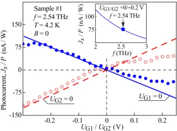
FIG. 3. Dependencies of the normalized magnitudeJxD/Pon the gate voltageUG1 (UG2) applied to the stripes at zero potential of the other gate UG2=0 (UG1=0). The polarization independent photocurrent contribution JxD is extracted from the photocurrent polarization dependencies (not shown). The data are obtained for (Cd,Mn)Te QW sample 1 at zero magnetic field. Here and in the further plots, except for the one showing results on scan across the sample, the data are presented for the laser beam focused on the DGG superlattice. Insets show experimental geometries. Here and in the further plots, the data are obtained for linearly polarized radiation with the electric field vectorE0xdirected perpendicularly to the metal gate fingers.
are shown in Fig. 2(b). Note that the application of gate voltages to individual gates does not visibly influence the period of 1/B oscillations of the longitudinal resistanceRxx
(not shown). This is due to the fact that the area of DGG fingers is a very small fraction of the whole sample area.
Moreover, the variation of bias voltage applied to gate 1 (UG1) also does not substantially affect the value ofRxx at a fixed magnetic field. The only detected deviation from the value ofRxx at zero gate voltages is an increase of the resistance by∼10% forUG2≈ −0.35 V. The gate voltage dependencies of the longitudinal resistance measured at one of the maxima of theRxx oscillations are shown in the inset in Fig. 2(b).
The dependencies are obtained at fixed magnetic field by sweeping the potential applied to one gate and holding the other one at zero bias. The observed behavior ofRxx will be addressed below in the discussion of photocurrent data. Note that while the overall characteristic of the data obtained at different cooldowns is the same the onset of the resistance increase can be shifted on the gate voltage scale by±0.1 V.
This is ascribed to cooldown dependent charge trapping in the insulator.
III. EXPERIMENTAL TECHNIQUE
For THz excitation we applied a continuous wave (cw) molecular optically pumped laser [46,47]. The laser operated at the frequencyf =2.54 THz (photon energy ¯hω=10.4 meV, wavelengthλ=118μm). The incident power about 30 mW was modulated at about 75 or 625 Hz by an optical chopper.
The radiation at normal incidence was focused onto a spot of about 1.3 mm diameter. The spatial beam distribution had an almost Gaussian profile, measured by a pyroelectric camera [48]. Taking into account the size of the superlattice we obtain that the power irradiating the structure is P ≈4 mW. The radiation intensity and electric field strength on the sample areI ≈300 mW/cm2andE0 ≈5.7 V/cm, respectively. Note that almost all experimental data, except the scan of the beam across the sample, are obtained for radiation focused on the DGG superlattice.
The structures were placed in a temperature variable optical magnetocryostat. The photocurrents were studied in the temperature range between 2 and 9 K. The laser radiation was linearly polarized along the x axis. The photoresponse is measured by the voltage drop U across a load resistor RL=50 OhmRs using standard lock-in technique. Here Rsis the sample resistance. The benefit of using of the small value of RL is that the detected signal is unaffected by the sample resistance variation and is just proportional to the electric current generated by the THz radiation. The current is calculated viaJ =U/RL.
IV. PHOTOCURRENT AT ZERO MAGNETIC FIELD We begin with briefly introducing the results obtained at zero magnetic field. While the paper is devoted to the obser- vation of magnetoratchet effect these results are important for further analysis of the data on magnetic field induced photocurrents.
Illuminating the DGG superlattice at normal incidence we have observed a photocurrent, whose magnitude and direction are sensitive to the electrostatic potentials applied to the first (G1) and the second (G2) gate sublattices. The photoresponse is detected perpendicularly to the gate stripes as well as along them. The fact that the photoresponse is generated by normally incident radiation provides a first indication that it is formed due to the presence of the superlattice.
Indeed it is well known that in unpatterned (001)-oriented QW structures a photocurrent signal is only detectable under oblique incidence [37,38]. The photocurrent consists of a contribution independent of the radiation polarization and a substantially smaller one dependent on the orientation of electric field vector E0 of the linearly polarized radiation in respect to the orientation of the gate stripes. This has been demonstrated by measuring the photocurrent as a function, the orientation of theE-field vector with respect to thexaxis (not shown). The same polarization behavior has been previously observed for the ratchet effect in lateral GaAs-based structures [14,21] as well as in DGG structures fabricated on top of InAlAs/InGaAs/InAlAs/InP high electron mobility transistors (HEMT) [29] and graphene [23].
For unbiased gates, a nonzero built-in electrostatic potential is formed due to the presence of metal stripes in the QW vicinity. A direct evidence for the ratchet effect comes from the variation of the photocurrent by application of the bias voltages to the individual gates. Indeed the ratchet effect is known to be proportional to the averaged product
=dV
dx|E(x)|2 (1)
of the derivative of the coordinate dependent electrostatic potential V(x) and the distribution of the electric near-field E(x) [15–17,20]. In the following, we call the parameter the lateral asymmetry. The value of may change sign depending on V(x). Consequently a variation of individual gate voltages should result in a change of the ratchet current including reversal of its direction, see the discussion in Sec.VI.
Exactly this behavior has been observed in the experiment.
In order to tune the lateral asymmetry, we applied different bias voltages UG1=UG2 to the grating gates. Figure 3 demonstrates the influence of the gate voltage variation on the amplitude and sign of the polarization independent photocurrentJxD[49]. Holding one of the gates at zero bias and varying the gate voltage on the other one we could controllably change the lateral asymmetry. The figure reveals that inversion of this lateral asymmetry obtained either by change of polarity of voltage applied to one gate or by interchange of gate voltage polarities applied to narrow and wide gates results in a change of sign of the photocurrent. This observation agrees well with the signature of ratchet currents: Jx ∝. Note that, while the overall characteristics of the data obtained at different cooldowns is the same, the photocurrent sign inversions can be shifted on the gate voltage scale by±0.1 V. Similarly to the results addressed in Sec.II Bthis is ascribed to cooldown dependent charge trapping in the insulator. We also note that for large negative gate voltages all contributions vanish, which can be attributed to closing the transistor channel beneath the metal stripes of the DGG superlattice. Figure3 also reveals that at large positive gate voltages the photocurrent saturates due to the effect of high electron densities.
To summarize, experiments at zero magnetic field provide a consistent picture demonstrating that the photocurrents are caused by the ratchet effect. They are (i) generated due to the lateral asymmetry, (ii) characterized by specific polarization dependencies for directions along and across the metal stripes, and (iii) change the direction upon reversing the lateral asymmetry. These results are in full agreement with the theory of ratchet effects excited by the polarized THz electric field in asymmetric lateral superlattices, discussed below in Sec.VI.
The overall behavior of the photocurrent is also in qualitative agreement with that of the electronic ratchet effects observed in semiconductor QW structures and graphene with a lateral superlattice [14,15,21,23].
V. MAGNETIC FIELD INDUCED PHOTOCURRENT A. Basic results
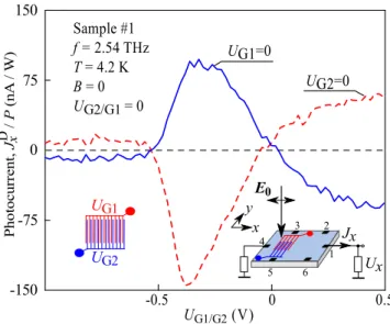
Now we turn to the main part of the paper devoted to magnetic field induced ratchet effects. Figure 4 shows the normalized photocurrent excited by linearly polarized radiation as a function of magnetic field applied perpen- dicularly to the QW plane. The principal observation is that with raising magnetic field the photocurrent drastically increases and, at high magnetic fields, exhibits sign-alternating 1/B-periodic oscillations. Moreover, Fig. 4 demonstrates that the reversal of the lateral asymmetry results in an inversion of the magnetophotocurrent direction providing a first clear indication that it is driven by the ratchet effect.
Measurements of the magnetophotocurrent as a function of
FIG. 4. Normalized photocurrent Jx/P as a function of the magnetic field B measured in (Cd,Mn)Te QW sample 1 for two combinations of the gate voltages. Solid blue line shows the data for the gate voltagesUG1=0 and UG2= −0.5 V and the dashed red line forUG1= −0.5 V andUG2=0, the setups denoted asUG1/G2= 0/−0.5 V andUG1/G2= −0.5/0 V. The vertical dashed line indicates zero magnetic field. The inset illustrates the experimental setup.
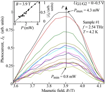
radiation power show that it scales linearly with the radiation power, i.e., quadratically with the radiation electric fieldE0, see inset in Fig. 5. Note that the positions of oscillation maxima/minima are independent of the radiation power, Fig.5.
Similar results, particularly magneto-oscillations with current amplitudes much larger than the photocurrent at B=0, are obtained for all studied samples. Studying various samples at different experimental conditions we found that the current in theydirection is much smaller thanJx.
FIG. 5. Magnetic field dependencies of the photocurrent |Jx| measured at different levels of power ranging from 0.8 to 4.3 mW in (Cd,Mn)Te QW sample 1. Inset shows radiation power dependence of the photocurrent amplitude|Jx|forB=3.9 T. Solid line is a linear fit.
FIG. 6. Normalized photocurrentJx/P measured as a function of magnetic fieldBin (Cd,Mn)Te QW sample 4 with the Dy grating.
Data from the (Cd,Mn)Te QW sample 4 with ferromagnetic Dy gate are shown in Fig.6. The period and magnitude of the 1/Boscillations correlate with transport behavior and are very close to those shown for (Cd,Mn)Te QW samples with gold DGG structure presented for sample 1, Fig.4.
Figure7shows another example of magnetophotocurrent measured for nonmagnetic CdTe QW sample 5 with gold DGG. While oscillations are clearly detected the signal is superimposed with a substantial background current. Because of the background the photocurrent, in contrast to samples 1 and 4, does not change sign with varying magnetic field.
The background photocurrent has also been obtained for (Cd,Mn)Te QW samples 2 and 3. We attribute an appearance of the background to imperfections of our large-size superlattices which are present in some structures as confirmed by optical microscope images [50]. The imperfections locally reduce symmetry and give rise to ratchet unrelated magnetogyrotropic photogalvanic currents in the “bulk” of the QW, see, e.g., Ref. [51].
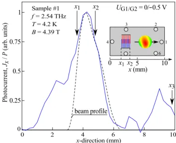
B. Laser beam scan across the DGG structure
To prove that the magnetoratchet effect stems from the irradiation of the superlattice we scanned the laser spot across the sample along thex direction. The photocurrent Jx was measured forB=4.39 T and the gate voltage combination UG1/G2=0/−0.5 V, i.e., at a maximum of one of the magneto-oscillations, Fig.4. The photocurrent generated by linearly polarized radiation with E0x as a function of the radiation spot position and the corresponding experimental geometry are shown in Fig.8. The photocurrent reaches its maximum for the laser spot centered at the superlattice and rapidly decays with the spot shifting away. For the beam spot touching the sample edge the current increases again. This is caused by an edge photocurrent [52] known for graphene [53,54] and semiconductor QWs [55]. Comparison with the laser beam spatial distribution measured by a pyroelectric camera (dashed curve in Fig. 8) shows that the change of the photocurrent for the scans across the DGG structure only slightly deviates from the Gaussian intensity profile. Note that
FIG. 7. (a) Normalized photocurrent Jx/P as a function of magnetic field B in CdTe-based QW sample 5 at two gate volt- age sequences:UG1/UG2= −2.5 V/0 andUG1/UG2=0/−2.5 V.
(b) and (c) Dependencies of the photocurrent magnitude on the gate voltageUG1(UG2) obtained for zero potential on the other gateUG2
(UG1). The data in (b) and (c) are obtained for the photocurrent maxima/minima atB= −4.9 and 4.9 T, respectively.
the DGG area is smaller than the beam spot. These findings unambiguously demonstrate that the photocurrent is caused by irradiation of the superlattice.
C. Effect of the lateral asymmetry variation of the photocurrent In order to explore the role of the lateral asymmetry, a pre- requisite for the ratchet photocurrents, we have systematically studied magnetophotocurrents for different combinations of the gate voltages. The results are shown for different samples in Figs.3,4,7, and9.
While the magnitude and the sign of the oscillations are strongly affected by the variation of the gate potentials the maxima/minima positions remain unchanged. To show that this conclusion is valid for the whole range of gate potentials used in our measurements we studied the photocurrent for a large set of different magnitudes and polarities of UG1 and UG2. These results are presented in the inset in Fig. 9forB ranging from 2.7 to 4.1 T.
Using the fact that maxima positions do not shift upon vari- ation ofBwe fixed the magnetic field and controllably varied
FIG. 8. Laser spot position dependence of the normalized pho- tocurrentJx/Pmeasured in (Cd,Mn)Te QW sample 1 at a maximum of the photocurrent oscillation atB=4.39 T andUG1=0,UG2=
−0.5 V. Inset shows the setup with the laser spot scanned along the x axis. Positions x1 and x2 correspond to the borders of the superlattice, whereasx3denotes the sample edge position. The dashed line represents the laser beam spatial distribution which is measured by a pyroelectric camera and scaled to the current maximum.
the lateral asymmetry by changing the potential applied to one of the gates and holding the other one at zero bias. Figures9(a) and9(b)show the results obtained for (Cd,Mn)Te QW sample 1 at magnetic field strengths 3.9 and−3.9 T, respectively. The figures reveal that the polarity of photocurrent changes with the sign of the asymmetry parameter, Eq. (1). This is primarily seen by comparing the curves obtained by variation of the potentials applied either to the thin (dashed lines) or thick (solid lines) gate stripes. The observed stronger change of the signal forUG1(UG2)≈ −0.35 V corresponds to an increase of the longitudinal resistance detected in magnetotransport measurements, see inset in Fig.2(b). It should be noted that, due to the above-mentioned built-in potential, the ratchet current can be detected even for zero gate voltages at both gates.
The same behavior upon variation of the lateral asymmetry has been observed for Dy-based DGG sample 4. Studying the photocurrent as a function of the gate voltage in CdTe QW sample 5 and in (Cd,Mn)Te samples 2 and 3 we obtained, that, despite the background, the photocurrent magnitude is also controlled by the lateral asymmetry. Corresponding results obtained for CdTe QW DGG structure 5 atB= ±4.9 T are shown in Figs.7(b)and7(c).
Now we turn to the analysis of the 1/Boscillations of the photocurrent which are obviously related to the SdH oscil- lations. Comparison with the magnetotransport data reveals that the period of the 1/B oscillations is indeed equal to that of the longitudinal magnetoresistance oscillations. This result is confirmed for all samples and temperatures used in our experiments. In the CdTe samples and (Cd,Mn)Te sample at relatively high temperatures the amplitude of oscillations grows with the magnetic field. This is shown for (Cd,Mn)Te
FIG. 9. Dependencies of the photocurrent magnitude on UG1 (UG2) obtained for zero potential on the other gateUG2(UG1). The data are obtained for (Cd,Mn)Te QW sample 1 atB=3.9 and−3.9 T, (a) and (b), respectively. The inset shows the magnetic field depen- dence of the photocurrent measured for different gate voltage combi- nations. Vertical dashed lines demonstrate that the maxima/minima positions of the magnetophotocurrent are not shifted for all gate voltage combinations. The numbers in the inset correspond to 1
→ UG1/G2=0/−0.5 V, 2→ UG1/G2= −0.5/0.5 V, 3→ UG1/G2= 0.5/0 V, 4→ UG1/G2= −0.5/−0.5 V, 5→ UG1/G2=0.5/−0.5 V, and 6→ UG1/G2= −0.5/0 V.
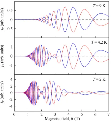
sample 1 in Fig. 10(a). By contrast, in diluted magnetic semiconductor (Cd,Mn)Te QW DGG samples at liquid helium temperature T =4.2 K the rise of the magnetophotocurrent amplitude at low fields is followed by its reduction at higher fields, see Fig. 10(b). At the lower temperature T =2 K this reduction, now detected at even lower magnetic fields, is followed by a further increase of the photocurrent magnitude at higher B, see data in Fig. 10(c). Similar “beats” of the magneto-oscillation amplitudes are detected for the longitudi- nal resistance, Fig.2, in agreement with the presence of the exchange enhanced Zeeman splitting in DMS materials [41].
The enhanced Zeeman splitting is caused by the exchange interaction between electrons and Mn2+ ions and described by the modified Brillouin function. The spin splitting first grows linearly with B and then saturates. The temperature increase leads to a decrease of giant Zeeman splitting caused by the exchange interaction and shifts the saturation to higher fields. All these features are detected in both transport and magnetophotocurrent experiments. Moreover, due to the enhanced spin splitting the oscillations measured at low temperatures and high magnetic fields become spin split which results in the beats.
FIG. 10. (a)-(c) Magnetic field dependence of the normalized photocurrentJx/P measured in (Cd,Mn)Te QW DGG sample 1 for three temperatures and two gate voltage combinations.
VI. DISCUSSION
In low-dimensional semiconductor structures with lateral superlattices, a dc electric current is generated due to the action of an electromagnetic wave’s ac electric field [33]. The effect of the superlattice is twofold: It generates a one-dimensional periodic electrostatic potential V(x) acting upon the 2D carriers withxbeing the superlattice principal axis, and causes a periodic spatial modulation of the THz electric field due to the near-field diffraction.
Figures11(a)and11(b)show coordinate dependence of the THz electric near-field Ex(x) calculated for the (Cd,Mn)Te QWs based DGG structure for two combinations of the gate voltages. The electric field distribution caused by the near- field diffraction is calculated for radiation with frequencyf = 2.54 THz applying a self-consistent electromagnetic approach based on the integral equation method described in detail in Ref. [56].
Figure11(c)shows the calculated THz absorption spectrum of the structure. It is seen that the plasmonic resonances in the
FIG. 11. (a) and (b) Electric near-fieldEx(x) normalized to the electric field of the incident THz wave. Shaded regions correspond to the positions of DGG metal fingers. Results are obtained for parameters of (Cd,Mn)Te QW sample 1 with dielectric constant =10 at the frequency 2.54 THz. The momentum relaxation timeτis obtained from the electron mobility specified in Sec.II. (c) Terahertz absorption spectrum of the structure. The inset shows the spectrum in the vicinity of the frequency 2.54 THz (indicated by vertical arrow) used in our experiments. The curve is calculated for the parameters used in (a) and (b).
QW are excited at frequencies well below the operation fre- quency of 2.54 THz. Therefore in the experimental frequency range the absorption follows the Drude law, see the inset in Fig.11(c). As a result, the near-field distribution in the QW shown in Figs.11(a)and11(b)is caused almost solely by the metal dual-grating gate and not by the plasma oscillations.
Hence one can neglect the dependence of the near field on the voltage applied to the DGG. Moreover, since the radiation frequency is much higher than that of plasmonic resonances we consider only electronic ratchet mechanism below.
The ratchet current is generated by a combined action on carriers of both the radiation near field, transmitted through the grating, and the periodic static potentialV(x) [14–16,21,23].
A crucial condition for dc electric current generation is that the lateral superlattice is asymmetric. Applying the voltages UG1andUG2in a controllable way, one can vary the potential V(x) and reverse the lateral asymmetry. Consequently, the ratchet photocurrent can also reverse its sign as observed in experiment, see Fig.3.
The ratchet current has components both perpendicular and parallel to the metal fingers and consists, in general, of polarization-independent, linear- and circular-ratchet con- tributions. All these individual ratchet currents have been
observed and described in various semiconductor-based struc- tures [14,15,21] as well as in graphene with lateral periodical top gates [16,23]. The mechanism leading to photocurrent formation can be illustrated on the polarization-independent photocurrent caused by the Seebeck ratchet (thermoratchet) effect. This contribution dominates at zero magnetic field (Sec. IV, Fig. 3) and, as we show below, is most rele- vant to the observed magnetic ratchet current. The Seebeck ratchet effect is caused by inhomogeneous heating of two- dimensional electron gas and subsequent relaxation of the electron temperature. Due to the near-field space modulation, the fieldE(x) acting upon electrons depends on the coordinate x, Figs. 11(a) and 11(b). The field heats the electron gas changing the effective electron temperature locally toT(x)= T +δT(x). Here we assume that, within a short time, the electron distribution becomes a quasiequilibrium Fermi-Dirac distribution with the temperatureT(x). The space-modulated temperature correction is defined by the energy balance and can be found from the following equation [16]:
kBδT(x)
τε =2|E(x)|2 e2
mω2τ. (2) Here kB is the Boltzmann constant, τε is the temperature relaxation time,τ is the momentum relaxation time,eis the electron charge, andmis the electron effective mass. We take into account that in the present experimentωτ ωcτ 1, whereωc= |eB|/(mc) is the cyclotron frequency.
As a result of the inhomogeneous heating, electrons diffuse from warmer to colder regions, and form a nonequilibrium density profile given by
δN(x) N = −π2
6 kBT
εF 2δT
T , (3)
whereN is the average electron density andεFis the Fermi energy. The ratchet current at zero magnetic field can be represented as a drift current of the electrons in the electric fieldE of the space modulated electrostatic potential V(x).
From Ohm’s lawj =σEwithE= −(1/e)dV /dxwe have j0= −eτ
mδN(x)dV
dx, (4)
where the bar denotes averaging over the superlattice period.
Finally, the ratchet current density at zero magnetic field is given by [16,33]
j0= π e3τεkBT
3mh¯2ω2εF, (5) whereis given by Eq. (1).
Figure12shows the photocurrent calculated after Eq. (5) together with the data of Fig. 3. The result of Fig. 12 is obtained for the near-field Ex(x) shown in Figs. 11(a) and 11(b). Parameters used for the calculations correspond to the sample 1. The only adjustable parameter is the temperature relaxation time taken asτε=4 ns. This value agrees with the temperature relaxation time of few nanoseconds reported for a degenerate electron gas in GaAs-based heterojunctions [57].
Figure12shows qualitative and reasonably good quantitative agreement between theory and experiment.
FIG. 12. Calculated dependencies of the photocurrentJx=j0w2
on the gate voltagesUG1(dashed line) andUG2(solid line) fitted to experimental curves shown in Fig.3(w2is defined in Fig.1). The lines are obtained after Eq. (5). To be specific, we used for calculationsE0 xin accordance with the experimental conditions. For the calculations we used the (Cd,Mn)Te DGG QW structure parameters discussed in Sec.II, electric near-fieldEx(x) shown in Figs.11(a)and11(b), lattice temperatureT =4.2 K, frequencyf =2.54 THz, and effective mass m=0.1m0. The only fitting parameter used here is the relaxation timeτε=4 ns. Inset shows the calculated frequency dependence of the photocurrentJx together with the experimental result forf = 2.54 THz (dot).
The above analysis suggests that, in the absence of magnetic field, the ratchet current is rather weak for degenerate electrons because, according to Eq. (3), the relative concentration cor- rectionδN/Nis much smaller than the temperature correction δT /T. Below we show that the situation changes drastically in the presence of a quantizing magnetic fieldBz.
The magnetic field induced ratchet currents in the directions perpendicularjxand paralleljyto the stripes of the superlattice are given by [33]
jx
j0 = 48ε2F
¯ hωckBT
(ωcτ)2 [1+(ωcτ)2]2
sinhz−zcoshz
sinh2z δ, (6) jy = − Bz
|Bz|
1+3(ωcτ)2
2(ωcτ)3 jx. (7) Here the magneto-oscillations are described by the factor δ (|δ| 1),
δ=cos 2π εF
¯ hωc
cos
π Z
¯ hωc
exp
− π ωcτ
, (8) while the dependence on z=2π2kBT /( ¯hωc) describes the oscillation suppression with increasing temperature, Eqs. (5)–
(7) are derived in the first order in δ. As compared with the theory developed in Ref. [33] we take into account the spin subband splittingZ due to the Zeeman effect. For the DMS-based ratchet structures the exchange enhanced Zeeman splitting is given by [38,41]
Z=g∗μBB+xS¯ 0N0αeB5/2
5μBgMn∗ B 2kB(TMn+T0)
, (9)
where g∗ is the electron Landé factor in the absence of magnetic impurities,μBis Bohr’s magneton, gMn∗ =2 is the Mngfactor,TMnis the Mn-spin system temperature,S0 and T0 are phenomenological fitting parameters [40,58],B5/2(ξ) is the modified Brillouin function, andN0αe is the exchange integral. Equations (6) and (7) predict that the ratchet current components jx and jy ∝jxBz have opposite parity upon magnetic field reversal due to the photocurrent deflection by the Lorentz force [59].
The ratchet current becomes an oscillating function of the magnetic field as the Landau levels move through the Fermi level and the photocurrent 1/B-oscillation period is the same as for SdH oscillations.
Equation (6) explains the reason for the ratchet current oscillations with a giantly enhanced magnitude as compared to the ratchet current at zero magnetic field. The crucial issue is that the ratchet current in a quantized magnetic field arises due to heating-induced corrections to the conductivity rather than a variation of the electron density, and the conductivity in this regime is extremely sensitive to electron temperature varia- tions. Indeed, even a weak change of the electron temperature near the Dingle temperature results in exponentially strong changes of the conductivity [60]. Therefore, the sensitivity of the conductivity to electron gas heating results in a huge enhancement of the ratchet current. The ratio j(B)/j0 is governed by a factor (εF/kBT)(εF/¯hωc) 1 and can reach about two orders of magnitude [33]. It should be stressed that this enhancement occurs in moderate fields where the resistance exhibits weak SdH oscillations. Heating damps the conductivity oscillations, therefore, depending on the sign of the correction, heating can either increase or decrease the conductivity because (∂σ/∂T) changes sign as a function ofB.
As a result, the heating-induced ratchet current is an oscillating function of the field with a zero mean value.
The calculated magnetic field dependencies of the ratchet currentsjx are shown in Fig. 13. The results are presented for two gate voltage combinations with equal magnitude but opposite sign of . Equations (5)–(7) reveal the most important features of the magnetic ratchet effect: the current is proportional to|E0|2, oscillates around zero with the same period as the longitudinal magnetoresistance, the amplitude of the current oscillations is immensely larger than the ratchet current at zero magnetic field, and the sign of the photocurrent reverses by changing the sign ofdV /dx. All these features have been observed experimentally, see Figs.4–7,9, and10.
Equations (6)–(8) also describe the more complicated oscillating ratchet current behavior observed in the DMS structures at low temperatures, see Figs. 10 and 13 for experiment and theory, respectively. In QWs without magnetic ions the second term in Eq. (9) is absent, the ratio ζ ≡ π Z/( ¯hωc) in Eq. (8) is independent of the magnetic field and reduces to (π/2)g∗(m/m0), wherem0is the free electron mass. In CdTe-based materials, ζ ≈ −0.26, the cosine of this value differs from unity by 3% and can be ignored. In the DMS structures, the presence of cosζ in Eq (8) results in the more complicated oscillating behavior of the ratchet current observed at low temperatures, see Figs. 10 and 13 for experiment and theory, respectively. Indeed, due to the temperature-dependent Brillouin function in the second term of Eq. (9) the Zeeman splitting becomes comparable to the
FIG. 13. Photocurrentjx calculated for (Cd,Mn)Te QW sample at three different temperatures. The structure parameters are relevant to the experiment presented in Fig. 4: εF=13 meV,μ=0.95× 104cm2/(V s) and ¯x=0.015. For other parameters we used the literature values forn−(Cd,Mn)Te :g∗= −1.64,N0αe=220 meV, see Ref. [41], andm=0.1m0, see Ref. [61]. For the calculations we also usedTMn=Tand literature data ofT0=0.8 K andS0=2.2 for
¯
x=0.015, see Ref. [62]. Solid and dashed curves show the results for two asymmetries of equal magnitudes but opposite signs of. The oscillation amplitude is much higher than the ratchet currentj0
at zero magnetic field (the latter is not seen at the chosen scale).
Landau levels separation at low temperatures and the doping with manganese plays a crucial role. Calculated curves for three values of the lattice temperatures and, consequently, different contributions of the Zeeman effect, are shown in Fig. 13. The calculations show, as in experiment, beats in the oscillations of jx(B). They stem from the interplay of Zeeman and Landau splittings and become more pronounced with decreasing temperature. Comparison of Figs.10and13 demonstrates that Eq. (6)–(8) describe the qualitative behavior of the photocurrent quite well. We note that the beats in jx,y(B) are substantially influenced by the Mn spin system temperature, which, because of electron gas heating, can be higher than the lattice temperature [63]. The heating, due to the strong dependence of the Brillouin function onTMn, results in a reduced contribution of the second term on the right-hand
side of Eq. (9) and shifts the onset of beats to higher magnetic fields.
Allowance for this effect should further improve the agreement between experimental data and calculations.
VII. SUMMARY
To summarize, we have experimentally demonstrated and theoretically explained the magnetic quantum ratchet effect, i.e., the ratchet effect in quantizing magnetic fields. To generate the ratchet current we use an asymmetric interdigitated top gate superlattice on top of the investigated quantum wells. Electric currents driven by terahertz electric field exhibit sign-changing magneto-oscillations with an amplitude giantly enhanced as compared to the photocurrent at zero magnetic field. The current amplitude and direction can be controllably changed by the variation of voltages applied to individual gate sublattices.
The effect is observed in structures with various QW composi- tions and superlattice parameters. The photocurrent generation mechanism can be well described in terms of semiclassical theory of magnetic ratchet effects. The observed effect is driven by the periodic modulation of the electron temperature caused by near-field diffraction. The theory of the Seebeck ratchet effect in the presence of quantizing magnetic field shows that the ratchet current follows the oscillations of the longitudinal resistance. In the DMS structures at low temperatures the investigated effect is strongly influenced by the exchange enhanced Zeeman splitting caused by the exchange interaction of electrons with Mn2+ions.
Finally we note, that while here we have dealt with a homogeneous magnetic field, the observed ratchet photocur- rent in superlattices made of hard magnetic material (Dy) opens a possibility to study the ratchet effect driven by an inhomogeneous periodic magnetic field recently suggested in Refs. [33,45]. This kind of experiments would apply remnant magnetization of Dy together with the enhanced magnetic properties of DMS QWs and is a future task.
ACKNOWLEDGMENTS
We thank I. A. Dmitriev and D. R. Yakovlev for helpful discussions. The support of the DFG priority program SFB 689 and Japanese-German joint research unit FOR 1483, the Volkswagen Stiftung Program and RFBR (Russia) via Projects No. 15-02-02989, No. 16-02-01037, No. 16-02-00375, and No. 17-52-53063 is gratefully acknowledged. The work of DVF was supported by the Grant from the President of the Russian Federation (No. MK-5447.2016.2). The research in Poland was partially supported by the National Science Centre (Poland) through Grant No. DEC-2012/06/A/ST3/00247 and by the Foundation for Polish Science through the IRA Programme co-financed by EU within SG OP.
[1] F. Jülicher, A. Ajdari, and J. Prost,Rev. Mod. Phys.69,1269 (1997).
[2] P. Reimann,Phys. Rep.361,57(2002).
[3] H. Linke,Appl. Phys. A: Mater. Sci. Process. A75,167(2002).
[4] P. Hänggi and F. Marchesoni,Rev. Mod. Phys.81,387(2009).
[5] S. Denisov, S. Flach, and P. Hänggi,Phys. Rep.538,77(2014).
[6] M. Büttiker,Z. Phys. B68,161(1987).
[7] Ya. M. Blanter and M. Büttiker,Phys. Rev. Lett.81,4040(1998).
[8] P. Reimann, M. Grifoni, and P. Hänggi,Phys. Rev. Lett.79,10 (1997).
[9] A. Lorke, S. Wimmer, B. Jager, J. P. Kotthaus, W. Wegscheider, and M. Bichler,Physica B249-251,312(1998).
[10] A. M. Songet al.,Appl. Phys. Lett.79,1357(2001).
[11] A. D. Chepelianskii, M. V. Entin, L. I. Magarill, and D. L.
Shepelyansky,Eur. Phys. J. B56,323(2007).
[12] A. D. Chepelianskii, M. V. Entin, L. I. Magarill, and D. L.
Chepelyansky,Physica E (Amsterdam)40,1264(2008).
[13] S. Sassine, Yu. Krupko, J.-C. Portal, Z. D. Kvon, R. Murali, K. P. Martin, G. Hill, and A. D. Wieck,Phys. Rev. B78,045431 (2008).
[14] P. Olbrich, E. L. Ivchenko, R. Ravash, T. Feil, S. D. Danilov, J. Allerdings, D. Weiss, D. Schuh, W. Wegscheider, and S. D.
Ganichev,Phys. Rev. Lett.103,090603(2009).
[15] E. L. Ivchenko and S. D. Ganichev,JETP Lett.93,673(2011).
[16] A. V. Nalitov, L. E. Golub, and E. L. Ivchenko,Phys. Rev. B86, 115301(2012).
[17] V. V. Popov,Appl. Phys. Lett.102,253504(2013).
[18] S. V. Koniakhin,Eur. Phys. J. B87,216(2014).
[19] I. V. Rozhansky, V. Yu. Kachorovskii, and M. S. Shur,Phys.
Rev. Lett.114,246601(2015).
[20] V. V. Popov, D. V. Fateev, E. L. Ivchenko, and S. D. Ganichev, Phys. Rev. B91,235436(2015).
[21] P. Olbrich, J. Karch, E. L. Ivchenko, J. Kamann, B. März, M.
Fehrenbacher, D. Weiss, and S. D. Ganichev,Phys. Rev. B83, 165320(2011).
[22] E. S. Kannan, I. Bisotto, J.-C. Portal, T. J. Beck, and L. Jalabert, Appl. Phys. Lett.101,143504(2012).
[23] P. Olbrich, J. Kamann, M. König, J. Munzert, L. Tutsch, J.
Eroms, D. Weiss, M.-H. Liu, L. E. Golub, E. L. Ivchenko, V. V.
Popov, D. V. Fateev, K. V. Mashinsky, F. Fromm, Th. Seyller, and S. D. Ganichev,Phys. Rev. B93,075422(2016).
[24] C. Drexler, S. A. Tarasenko, P. Olbrich, J. Karch, M. Hirmer, F. Müller, M. Gmitra, J. Fabian, R. Yakimova, S. Lara-Avila, S.
Kubatkin, and S. D. Ganichev,Nat. Nanotechnol.8,104(2013).
[25] T. Watanabe, S. A. Boubanga-Tombet, Y. Tanimoto, D. Fateev, V. Popov, D. Coquillat, W. Knap, Y. M. Meziani, Y. Wang, H.
Minamide, H. Ito, and T. Otsuji,IEEE Sens. J.13,89(2013).
[26] Y. Kurita, G. Ducournau, D. Coquillat, A. Satou1, K. Kobayashi, S. Boubanga Tombet, Y. M. Meziani, V. V. Popov, W. Knap, T.
Suemitsu, and T. Otsuji,Appl. Phys. Lett.104,251114(2014).
[27] S. A. Boubanga-Tombet, Y. Tanimoto, A. Satou, T. Suemitsu, Y. Wang, H. Minamide, H. Ito, D. V. Fateev, V. V. Popov, and T. Otsuji,Appl. Phys. Lett.104,262104(2014).
[28] V. V. Popov, D. V. Fateev, T. Otsuji, Y. M. Meziani, D. Coquillat, and W. Knap,Appl. Phys. Lett.99,243504(2011).
[29] P. Faltermeier, P. Olbrich, W. Probst, L. Schell, T. Watanabe, S. A. Boubanga-Tombet, T. Otsuji, and S. D. Ganichev,J. Appl.
Phys.118,084301(2015).
[30] S. D. Ganichev, W. Weber, J. Kiermaier, S. N. Danilov, P.
Olbrich, D. Schuh, W. Wegscheider, D. Bougeard, G. Abstreiter, and W. Prettl,J. Appl. Phys.103,114504(2008).
[31] S. N. Danilov, B. Wittmann, P. Olbrich, W. Eder, W. Prettl, L. E.
Golub, E. V. Beregulin, Z. D. Kvon, N. N. Mikhailov, S. A.
Dvoretsky, V. A. Shalygin, N. Q. Vinh, A. F. G. van der Meer, B. Murdin, and S. D. Ganichev,J. Appl. Phys.105,013106 (2009).
[32] S. Dvoretsky, N. Mikhailov, Y. Sidorov, V. Shvets, S. Danilov, B. Wittman, and S. Ganichev,J. Electron. Mater.39,918(2010).
[33] G. V. Budkin, L. E. Golub, E. L. Ivchenko, and S. D. Ganichev, JETP Lett.104,649(2016).
[34] S. A. Crooker, D. A. Tulchinsky, J. Levy, D. D. Awschalom, R. Garcia, and N. Samarth, Phys. Rev. Lett. 75, 505 (1995).
[35] J. C. Egues and J. W. Wilkins,Phys. Rev. B 58, R16012(R) (1998).
[36] J. Jaroszynski, T. Andrearczyk, G. Karczewski, J. Wróbel, T.
Wojtowicz, E. Papis, E. Kaminska, A. Piotrowska, D. Popovic, and T. Dietl,Phys. Rev. Lett.89,266802(2002).
[37] S. D. Ganichev, S. A. Tarasenko, V. V. Bel’kov, P. Olbrich, W. Eder, D. R. Yakovlev, V. Kolkovsky, W. Zaleszczyk, G.
Karczewski, T. Wojtowicz, and D. Weiss,Phys. Rev. Lett.102, 156602(2009).
[38] P. Olbrich, C. Zoth, P. Lutz, C. Drexler, V. V. Bel’kov, Ya. V.
Terent’ev, S. A. Tarasenko, A. N. Semenov, S. V. Ivanov, D. R.
Yakovlev, T. Wojtowicz, U. Wurstbauer, D. Schuh, and S. D.
Ganichev,Phys. Rev. B86,085310(2012).
[39] M. K. Kneip, D. R. Yakovlev, M. Bayer, G. Karczewski, T. Wojtowicz, and J. Kossut, Appl. Phys. Lett. 88, 152105 (2006).
[40] J. A. Gaj, R. Planel, and G. Fishman,Solid State Commun.29, 435(1979).
[41] J. K. Furdyna,J. Appl. Phys.64,R29(1988).
[42] T. Dietl, inHandbook on Semiconductors, edited by T. S. Moss (North-Holland, Amsterdam, 1994), Vol. 3b.
[43] J. Kossut and J. A. Gaj (eds.), Introduction to the Physics of Diluted Magnetic Semiconductors(Springer, Berlin, 2010).
[44] M. Staab, M. Matuschek, P. Pereyra, M. Utz, D. Schuh, D.
Bougeard, R. R. Gerhardts, and D. Weiss, New J. Phys.17, 043035(2015).
[45] G. V. Budkin and L. E. Golub, Phys. Rev. B 90, 125316 (2014).
[46] J. Karch, P. Olbrich, M. Schmalzbauer, C. Zoth, C. Brin- steiner, M. Fehrenbacher, U. Wurstbauer, M. M. Glazov, S. A.
Tarasenko, E. L. Ivchenko, D. Weiss, J. Eroms, R. Yakimova, S.
Lara-Avila, S. Kubatkin, and S. D. Ganichev,Phys. Rev. Lett.
105,227402(2010).
[47] Z. D. Kvon, S. N. Danilov, N. N. Mikhailov, S. A. Dvoretsky, and S. D. Ganichev,Physica E40,1885(2008).
[48] E. Ziemann, S. D. Ganichev, I. N. Yassievich, V. I. Perel, and W. Prettl,J. Appl. Phys.87,3843(2000).
[49] Note that inxdirection the polarization independent contribu- tionJxDdominates the photocurrent for all studied samples and almost all combinations of gate voltages applied to the individual subgratings of DGG.
[50] Fabrication of such a large-size superlattices is a challenging task. Therefore, some of our structures have minor imperfec- tions, as confirmed by optical microscope images. The imper- fections occur on samples with occasional inhomogeneities of the PMMA resist. Due to that the electron beam lithography was unable to write the exact width of the stripes as it was intended and, therefore, ended up with an overlap of the Au fingers.
This leads to short circuits, as well as to complete destruction of few gate fingers by removing the additional Au material in the finger spacings. In some of our structures the connection between two gate stripes also showed up when surface impurities were covered with Au, which were not supposed to be part of the gate fingers.
[51] V. V. Bel’kov and S. D. Ganichev,Semicond. Sci. Technol.23, 114003(2008).
[52] The edge photocurrent is caused by the asymmetric scattering of carriers driven back and force to the edge by the radiation electric field [53,54].
[53] J. Karch, C. Drexler, P. Olbrich, M. Fehrenbacher, M. Hirmer, M. M. Glazov, S. A. Tarasenko, E. L. Ivchenko, B. Birkner, J.
Eroms, D. Weiss, R. Yakimova, S. Lara-Avila, S. Kubatkin, M.
Ostler, T. Seyller, and S. D. Ganichev,Phys. Rev. Lett.107, 276601(2011).
[54] M. M. Glazov and S. D. Ganichev,Phys. Rep.535,101(2014).
[55] K.-M. Dantscher, D. A. Kozlov, M. T. Scherr, S. Gebert, J.
Bärenfänger, M. V. Durnev, S. A. Tarasenko, V. V. Bel’kov, N. N. Mikhailov, S. A. Dvoretsky, Z. D. Kvon, D. Weiss, and S. D. Ganichev,arXiv:1612.08854.
[56] D. V. Fateev, V. V. Popov, and M. S. Shur,Semiconductors44, 1406(2010).
[57] T. Kawamura, S. Das Sarma, R. Jalabert, and J. K. Jain,Phys.
Rev. B42,5407(1990).
[58] J. Kossut and J. A. Gaj (eds.),Introduction to the Physics of Diluted Magnetic Semiconductors(Springer, Berlin, 2011).
[59] K.-M. Dantscher, D. A. Kozlov, P. Olbrich, C. Zoth, P.
Faltermeier, M. Lindner, G. V. Budkin, S. A. Tarasenko, V. V.
Bel’kov, Z. D. Kvon, N. N. Mikhailov, S. A. Dvoretsky, D.
Weiss, B. Jenichen, and S. D. Ganichev,Phys. Rev. B92,165314 (2015).
[60] C. Hamaguchi,Basic Semiconductor Physics(Springer, Berlin, 2014).
[61] A. A. Dremin, D. R. Yakovlev, A. A. Sirenko, S. I. Gubarev, O. P.
Shabelsky, A. Waag, and M. Bayer,Phys. Rev. B72,195337 (2005).
[62] W. J. Ossau and B. Kuhn-Heinrich, Physica B 184, 422 (1993).
[63] D. Keller, D. R. Yakovlev, B. König, W. Ossau, Th. Gruber, A.
Waag, L. W. Molenkamp, and A. V. Scherbakov,Phys. Rev. B 65,035313(2001).