Terahertz Laser Induced Ratchet
Effects and Magnetic Quantum Ratchet Effects in Semiconductor
Nanostructures
DISSERTATION
zur Erlangung des Doktorgrades der Naturwissenschaften doctor rerum naturalium
(Dr. rer. nat.) Fakult¨at f¨ur Physik Universit¨at Regensburg
vorgelegt von
Philipp Faltermeier
aus Mallersdorf-Pfaffenberg
im Jahr 2017
Die Arbeit wurde von Prof. Dr. Sergey D. Ganichev angeleitet.
Das Promotionsgesuch wurde am 8. Juni 2017 eingereicht.
Pr¨ ufungsausschuss:
Vorsitzende: Prof. Dr. Milena Grifoni 1. Gutachter: Prof. Dr. Sergey D. Ganichev 2. Gutachter: PD Dr. Tobias Korn
weiterer Pr¨ufer: Prof. Dr. Christian Sch¨uller
Contents
1 Introduction 5
2 Physical Background 8
2.1 Basics of the Ratchet Effect . . . . 8
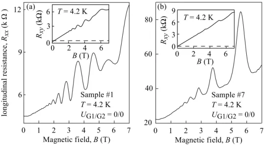
2.2 Longitudinal Magneto-Resistance Oscillations . . . 13
2.3 Diluted Magnetic Semiconductor . . . 17
3 Experimental Methods 19 3.1 Optically Pumped Molecular THz Laser . . . 19
3.2 Microwave Radiation Generation . . . 22
3.3 Variation of Radiation’s Polarization State . . . 22
3.4 Experimental Setup . . . 27
4 Sample Preparation and Characteristics 31 4.1 CdTe and (Cd,Mn)Te Samples . . . 31
4.1.1 Sample Growth . . . 32
4.1.2 Structure Design . . . 33
4.1.3 Electron Beam Lithography and Optical Lithography . . 35
4.1.4 Thermal Evaporating and Lift-off . . . 37
4.1.5 Ohmic Contacts . . . 37
4.1.6 CdTe and (Cd,Mn)Te Quantum Well Characterization . 38 4.2 High Electron Mobility Transistor Samples . . . 42
4.2.1 Sample Growth . . . 42
4.2.2 Fabrication of Double Interdigitated Grating Gates . . . 43
4.2.3 HEMT Sample Characterization . . . 44
CONTENTS 4 5 Ratchet Effect at Zero Magnetic Field in (Cd,Mn)Te QWs 45 5.1 Experimental Results and Discussion . . . 45 5.2 Microscopic Theory and Comparison with Experiments . . . 50 5.3 Brief Summary . . . 56 6 Magnetic Quantum Ratchet Effect in CdTe and (Cd,Mn)Te
QWs 57
6.1 Experimental Results and Discussion . . . 57 6.2 Microscopic Theory and Comparison with Experiments . . . 66 6.3 Brief Summary . . . 70 7 Polarization Sensitive Magnetic Quantum Ratchet Effect 71 7.1 Experimental Results and Discussion . . . 71 7.2 Microscopic Theory and Comparison with Experiments . . . 78 7.3 Brief Summary . . . 82 8 Helicity Sensitive THz Radiation Detection by InGaAs High
Electron Mobility Transistors 83
8.1 Experimental Results . . . 83 8.2 Discussion . . . 90 8.3 Brief Summary . . . 92
9 Conclusion 93
Appendix 95
References 98
1 Introduction
The classical ratchet and the quantum ratchet effects occur in spatially peri- odic non-centrosymmetric systems which are able to transport non-equilibrium particles in the absence of an average macroscopic force [1–5]. By driving such systems out of thermal equilibrium, for example by high frequency alternating electric fields, a direct electric current is generated in semiconductors and semi- conductor nanostructures [6–20]. The requirement of a non-centrosymmetric system can be fulfilled by either making use of an in-built asymmetry induced by a crystallographic structure (in this case ratchet effects are called photogal- vanic effects [11, 15, 21]) or by an artificial structure superimposed on typically two-dimensional semiconductor materials [11, 13, 14, 22–25]. Such structures were realized on semiconductor quantum wells [14,15,22,26] and on top of gra- phene [27, 28]. These experiments demonstrate that, in particular, the ratchet effects are efficiently excited by terahertz radiation. Based on the experimental data, the basic physics of the ratchet effect in low dimensional electron systems was explored, providing information on the non-equilibrium transport in these systems. The influence of the magnetic field, however, as well as the ratchet effect as possibility for detecting the terahertz radiation’s polarization states were not considered up to now.
The core of this thesis is to investigate the influence of the magnetic field on the
ratchet effects, which are generated by the terahertz radiation. The terahertz
electric field and the external magnetic field in combination with the lateral
asymmetric dual grating gate structure on top of the quantum well structure
give rise to several new effects which will be investigated in this thesis. One
of these effects is that the generated current exhibits sign-alternating 1/B-
periodic oscillations with amplitudes by orders larger than the ratchet current
at zero magnetic field. Further, it will be shown that the sign and the am-
plitude of the magnetic quantum ratchet current can be effectively controlled
by the applied gate voltages. Moreover, it will be demonstrated that different
directions of the linearly polarized radiation, as well as left-handed and right-
handed circularly polarized radiation, can change the amplitude and even the
sign of the current oscillations. These new effects are observed in CdTe and in
diluted magnetic semiconductor (Cd,Mn)Te quantum wells. The latter mate-
1 INTRODUCTION 6 rial leads to enhanced spin related phenomena due to the exchange interaction of the electrons with manganese (Mn
2+). This interaction allows to explore the role of the spin ratchet effect [29] by changing either the temperature, the magnetic field or the potentials induced by the voltages applied to the top gate structure. Since these materials were not investigated for ratchet effects up to now, the ratchet currents at zero magnetic field are also investigated. The ob- tained experimental phenomena are discussed by terms of the simultaneously developed theory.
The fact that the ratchet current is alterable by different gate voltages and also by different polarization states of the radiation, provides the basis for the development of a polarization sensitive detector. In this work, an In- AlAs/InGaAs/InAlAs/InP based high electron mobility transistor was cho- sen as detecting material [23–25, 30] which has previously been shown to be a good material for detection. Although, the recently developed tera- hertz detectors based on field effect transistors are focused on single gated structures, several groups demonstrated that higher sensitivities are antici- pated for structures with periodic symmetric and asymmetric metal stripes or gates [13, 17, 23, 26, 30–34].
In this thesis, it will be demonstrated that the generated direct photocurrent, excited by terahertz radiation in a dual grating gate InGaAs high electron mobility transistor, is sensitive to the radiation helicity and the linear polar- ization state of the radiation. These phenomena are well described in terms of the ratchet effects [15–17, 22, 30] excited in two dimensional electron sys- tems with a spatially periodic dc in-plane potential [17, 19, 23]. Furthermore, it will be shown that single photocurrent contributions, e.g. those induced by the helicity of the radiation, can be turned on and off by a proper choice of the voltages applied to the top gate structure. In particular, the photocur- rent changes its direction by inverting the polarization helicity. These effects open up new possibilities for an all-electric detector for the terahertz radiation polarization state at room temperature.
The thesis is organized as follows: In Chap. 2, the theoretical background,
which serves as a basis for the study of the magnetic ratchet effect as well as
1 INTRODUCTION 7
the ratchet effect in the terahertz detection, is presented. The theoretical back-
ground includes the basic principle of the ratchet effect and the longitudinal
magneto-resistance, as well as a description of the diluted magnetic semicon-
ductors. The experimental methods are discussed in Chap. 3, containing a brief
introduction of the used radiation sources, as well as the Stokes parameters of
the radiation’s polarization state and the methods for its variation. Chapter 4
is dedicated to the samples, including their growth, the processing of the top
gate structures and their characterization. In Chap. 5, the experimental results
of the polarization independent and polarization dependent ratchet effect at
zero magnetic field are presented, as well as the microscopy theory and a short
summary. Next follows an investigation of the magnetic quantum ratchet effect
in Chap. 6, starting with the experimental results and discussion, the semiclas-
sical theory and a summary in the last section. The data and theory for the
polarization sensitive magnetic quantum ratchet effect are shown and discussed
in Chap. 7. The ratchet effect as terahertz radiation detector is presented in
Chap. 8, whilst Chap. 9 gives a summary of the whole work.
2 Physical Background
The magnetic quantum ratchet effect (MQRE), which is observed and explored in this work, is based on different physical models. To aid understanding, these models will be briefly discussed in this chapter. After describing the ratchet effect in semiconductor heterostructures with lateral top gate potentials, the longitudinal magneto-oscillations - describing the oscillating behavior of the MQRE in the magnetic field B - will be explained. In addition, as most expe- riments for the MQRE were carried out on diluted magnetic semiconductors (DMS), the influence of the DMS materials will be briefly introduced.
2.1 Basics of the Ratchet Effect
The ratchet effect is generally known as the generation of a direct current, in- duced by a terahertz (THz) radiation in two-dimensional (2D) semiconductor systems with an asymmetric top gate structure. The common idea is that a non-equilibrium spatially periodic non-centrosymmetric system is able to transport particles under the influence of an oscillating force, which is zero in average [7, 14–16, 22, 28, 35, 36].
Blanter and B¨uttiker introduced a model describing the motion of particles in a periodic potential and their exposure to a periodic temperature modula- tion [7]. Figure 2.1(a) shows a schematic drawing of their considered system.
In this system, a superlattice is irradiated through a mask of the same period, but phase shifted with respect to the superlattice [6]. This spatially modulated irradiation leads to a locally modulated electron gas heating inducing a tem- perature gradient in the two-dimensional electron gas (2DEG). The influence of this gradient yields to a direct current of the charge carriers.
A possible realization of this system with small variations of the top structure is shown in Fig. 2.1(b). The superlattice is replaced by a lateral periodic potential induced by a non-centrosymmetric metal grating on top of the sample surface.
Therefore, the in-plane modulation of the radiation does not appear via a
mask with periodic structures but instead due to the near-field effect of the
THz radiation propagating through the metal grating [22]. This near-field
diffraction heats the electron gas locally.
2 PHYSICAL BACKGROUND 9
Figure 2.1: (a) Idea to realize a electronic ratchet by Blanter and B¨ ut- tiker [7, 14]. Superlattice irradiated through a mask of the same period but phase shifted with respect to the underlying superlattice. (b) shows one pos- sible realization of this idea with metallic gate stripes on top of the sample (adapted from [14, 22]).
A theoretical model for the phenomenological description of the ratchet effect, following the descriptions in Refs. [15, 22, 35], will be given here. The consid- ered structure has a quantum well with an one-dimensional periodic potential V (x) on top of the surface with the property V (x) = V (x + d) and the period d. The coordinate system is defined in Fig. 2.1, with the x- and y-directions lying in the quantum well (QW) plane, the z-axis being parallel to the growth direction and pointing against the propagation of the radiation. The radia- tion shining on the QW is an alternating time dependent in-plane electric field E(x, t), described as
E(x, t) = E
ω(x)e
−iωt+ E
ω∗(x)e
iωt,
with the radiation frequency ω, the time t and the amplitude E
ω(x) modulated along the x-direction and with the same period as the static lateral potential, E
ω(x) = E
ω(x + d). The electric field E
ω(x) and the potential V (x) can be written in a general form [15, 22]:
E
ω(x) = E
0"
1 +
∞
X
n=1
h
ncos (nqx + ϕ
E,n)
# , V (x) =
∞
X
n=1
V
ncos (nqx + ϕ
V,n) ,
(2.1)
with the phases for the electric field ϕ
E,nand the potential ϕ
V,n. The coordinate independent amplitude of the electric field is given by E
0. The coefficients h
nand V
nare real values, n is an integer number and q is 2π/d.
2 PHYSICAL BACKGROUND 10 The ratchet effect will be described by using the classical Boltzmann equation for the electron distribution function f
k(x, t), as provided in Ref. [15,22]. The Boltzmann equation can be used when the potential V (x) is weak and smooth, satisfying | V (x) | ≪ ε
eand q ≪ k. The electron energy ε
eis defined as ε
e= ~
2k
2/2m
∗with the Planck constant ~ , the electron wave vector k and the effective mass m
∗. The typical electron energy ε
ehas to be much larger than the photon energy ~ ω, which is fulfilled in the THz frequency range. The Boltzmann equation is given by [15, 22]
∂
∂t + v
k,x∂
∂x + F (x, t)
~
∂
∂ k
f
k(x, t) + Q
k= 0, (2.2) where v
k= ~ k/m
∗is the electron velocity and k = (k
x, k
y) is lying in the QW plane. Q
kis the collision integral and the force F (x, t) consists of two terms:
F (x, t) = − dV (x)
dx e ˆ
x+ eE(x, t),
with the electron charge e and the unit vector e ˆ
xalong the x-direction. The collision integral Q
kis the sum of the energy relaxation and the elastic scat- tering terms (for more information, see Refs. [15, 22]).
From the Boltzmann equation, the average electron current j is calculated which is given in the following equation:
j = 2e X
k
v
kf
k. (2.3)
The bar over the electron distribution function f
kmeans averaging over the spatial coordinate x and time t. The prefactor 2 stems from the electron spin degeneracy.
The current j is obtained by solving the classical Boltzmann Eq. (2.2). There- fore, the electron distribution function f
k(x, t) is expanded in third order per- turbation theory. This means the function is expanded up to the second order in powers of the radiation electric field and in the first order of the static lateral potential V (x):
f
k(x) = f
k(0)(x) + f
k(1)(x, t) + f
k(2)(x, t) . (2.4)
The first term, f
k(0)(x), is the equilibrium distribution function and f
k(1)(x, t) de-
pends linearly on the electric field E(x, t). The last term, f
k(2)(x, t), is quadratic
2 PHYSICAL BACKGROUND 11 in E(x, t) and, therefore, linear in the intensity of the radiation. For further calculations only the time-independent contribution f
k(2)(x) = ξ
k(x) is neces- sary. The electron distribution function in Eq. (2.3) is substituted by Eq. (2.4).
By successive iteration of the kinetic equation Eq. (2.2) and summing over all k, the current can be written as:
j = µ
e(
δN(x) dV (x)
dx e ˆ
x+ 2 | e | Re[E
ω∗(x)δN
ω(x)]
)
. (2.5)
Here, µ
e= | e | τ /m
∗is the electron mobility with the momentum relaxation time τ . The spatially modulated electron densities are given by
δN(x) = 2 X
k
ξ
k(x) and δN
ω(x) = 2 X
k
f
k(1)ω(x).
The first term on the right hand side in Eq. (2.5) describes the polarization independent Seebeck ratchet effect and the second term is the polarization dependent ratchet effect. Several assumptions have to be made to allow further calculations of the ratchet current, namely [15, 22]:
• the energy relaxation time τ
εis larger than the momentum relaxation time τ and the inverse frequency ω
−1• the electron mean free path l
e= v
Tτ and the energy diffusion length l
ε= v
T√ τ τ
εare both small compared to the superlattice period d. The thermal velocity v
Tis given by v
T= p
2k
BT /m
∗with the Boltzmann constant k
Band the temperature T
• the influence of ac diffusion on first-order amplitudes f
k(1)ω(x, t) is ne- glected, which is correct for v
Tq ≪ ω
• no restrictions on the value of the product ωτ
The Seebeck ratchet current contains the static correction δN(x) of the spa-
tially modulated electron density. The spatially modulated radiation heats the
two-dimensional electron gas, which changes the effective temperature of the
electron gas from the equilibrium value T to T (x) = T
e+ δT (x). Here, T
eis
the average electron temperature and the temperature correction term δT (x)
2 PHYSICAL BACKGROUND 12 oscillates in space with the period d [16]. The temperature gradient, caused by δT (x), leads to a redistribution of the electron density δN (x) and therefore to an appearance of an electric-field-induced static correction of δN (x) [22].
Further, δT (x) causes an inhomogeneous correction to the conductivity, lead- ing to a direct current which is independent of the polarization state of the radiation.
The polarization dependent ratchet current can be calculated when the sec- ond term in Eq. (2.5) is taken into account. The spatially modulated electron density δN
ω(x) is time-dependent and satisfies the continuity equation. From the continuity equation, it follows that - when calculating the current j - it is sufficient to find a correction to δN
ω(x). This correction contribution is linear in the lateral potential and replaces E
ω(x) by a non-modulated electric field E
0[15, 22]. Taking the average over the x-direction and time t of the spatially modulated electron density δN
ω(x) and the electric field E
ω∗(x) leads to the polarization dependent ratchet photocurrent.
The ratchet current can be written as the sum of the polarization indepen- dent Seebeck ratchet and the polarization dependent ratchet effect. Therefore, Eq. (2.5) can be further treated by averaging over the x-direction and con- sidering the modulated electron densities. The polarization independent and dependent ratchet currents in x- and y-direction are given by [15, 22]
j
x= ¯ I[χ
1+ χ
2( | e ˆ
x|
2− | e ˆ
y|
2)] ,
j
y= ¯ I[χ
3(ˆ e
xe ˆ
∗y+ e ˆ
ye ˆ
∗x) − γP
circe ˆ
z] , (2.6) with P
circe ˆ
z= i(ˆ e
xe ˆ
∗y− e ˆ
ye ˆ
∗x). The average light intensity ¯ I is defined by
I ¯ = cn
ω2π ( | E
0x|
2+ | E
0y|
2) ,
with the speed of light in vacuum c and the frequency dependent refractive index n
ω. The remaining coefficients are
χ
2= χ
3= − ωτ γ, χ
1= (4τ
ǫ− τ)ωγ , with
γ = ζ πe
2~ cn
ω~ q m
∗V
1k
BT
µ
eN
0τ
ω(1 + ω
2τ
2) .
2 PHYSICAL BACKGROUND 13 Here, ζ = h
1sin (ϕ
V− ϕ
E) is called the asymmetry parameter and N
0is the x-independent electron density. The Seebeck ratchet current is represented by the coefficient χ
1, whilst the linear ratchet effect is attributed to χ
2( | e ˆ
x|
2−| e ˆ
y|
2) and χ
3(ˆ e
xe ˆ
∗y+ e ˆ
ye ˆ
∗x). The circular polarization sensitive ratchet current is de- scribed by γP
circe ˆ
z.
In the ratchet current, the phase shift ζ is included in all coefficients χ
1, χ
2, χ
3and γ. Therefore, (ϕ
V− ϕ
E) 6 = nπ is necessary to obtain a current, with n as an integer number. The phase shift is achieved when the electric field and the potential are out of phase with respect to each other.
In order to clarify the contribution of the intensity of the electric field | E(x) |
2and the variation of the potential ∂V /∂x on the current generation, the equa- tion for the ratchet currents can be rewritten. The current j
x/ycan be ex- pressed as [16, 22]:
j
x/y∝ Ξ with
Ξ = qV
1h
1E
02sin(ϕ
V− ϕ
E) = | E(x) |
2∂V
∂x . (2.7)
Thereby, the simplest form of the electric field and lateral-potential modulation from Eq. (2.1) for n = 1 is taken into account. The parameter Ξ will be treated as lateral asymmetry and its value may change its sign due to changes of the potential V (x) [37].
2.2 Longitudinal Magneto-Resistance Oscillations
The longitudinal magneto-resistance oscillations can be observed in a two-
dimensional electron gas when high magnetic fields are applied perpendicularly
to the two-dimensional quantum well plane at low temperatures. One of the
characteristics of the 2DEG is that the motion of the electrons in growth di-
rections of the quantum well is quantized, but the electrons can move in the
QW plane without restrictions. Under application of a magnetic field, how-
ever, the electron energy spectrum is additionally quantized, forming discrete
Landau levels. Thereby, each Landau level is connected to a separated δ-peak
2 PHYSICAL BACKGROUND 14 in the density of states ν
±for the condition k
BT < ~ ω
c[38]. Here, the angular frequency is ω
c= eB/m
∗with the magnetic field B.
Even though, the Landau levels (LL) and, therefore, the peaks of the density of states are broadened in a realistic system due to both finite temperatures and scattering processes, they can be separated, as illustrated in Fig. 2.2(a).
Figure 2.2: (a) depicts a schematic view of density of states ν
±for fixed magnetic field B = B
1with Landau level splitting ∆E
l,l+1and Zeeman splitting ∆E
Z. (b) shows a sketch of spin split Landau levels as a function of B. The magnetic field B
1and the Fermi energy E
Fare marked as black solid lines (adapted from [39]).
The energy of the l-th Landau level can be calculated for a parabolic energy spectrum using the following equation [39]:
E
l= ~ ω
c(l + 1
2 ) , (2.8)
with l as an integer number. The energy-related distance between two neigh- boring Landau levels l and l ± 1 is given by ∆E
l,l±1= ~ ω
c.
The application of a sufficiently strong magnetic field B additionally splits the Landau levels according to the electron spin. This phenomenon is called Zee- man effect, resolving energetically the degenerated spin states in the Landau levels. This difference in energy is given by
∆E
Z= gµ
BB, (2.9)
2 PHYSICAL BACKGROUND 15 with the Land´e factor g of the material and the Bohr magneton µ
B[39]. Taking into account the Zeeman splitting, the number of carriers on each spin split Landau level is given by n
LL= | e | B/h, see Ref. [39]. The number of filled Zeeman split Landau levels is called filling factor v. When considering an electron gas with a carrier density N
s, the filling factor v is given by [39]:
v = N
sn
LL= N
sh
| e | B . (2.10)
For a fixed carrier density N
s, the Fermi energy E
Foscillates as a function of the applied magnetic field B [39,40] as shown in Fig. 2.2(b). These oscillations of the Fermi energy rely on the density of states ν
±[38]. In an example where the Landau level l is completely filled and the (l + 1) level is only partly filled, the Fermi energy E
Flies within the energetically higher (l + 1) Landau level, see Fig. 2.2(a). If the magnetic field B is increased, the energy of the (l + 1) Landau level rises and is emptied, due to the increasing degeneration of the lower Landau levels. Therefore, the Fermi energy drops back down to the l-th Landau level [38]. This is illustrated in Fig. 2.2(b), which shows the oscillation of the Fermi energy in an ideal system with δ function Landau levels. Beyond that, the oscillations of the Fermi energy E
Fresult in a changing of the fill- ing factor v. If the magnetic field B is changed, the Landau levels and the connected density of states are shifted through the Fermi energy, resulting in a 1/B-periodic oscillation. This can also be achieved by varying the Fermi energy and keeping the magnetic field at a fixed value.
Figure 2.2(a) shows that the density of states ν
±at the Fermi energy level E
Fvaries with changes to the magnetic field B. The density of states is zero when the Fermi energy lies in between two Landau levels, but reaches a maximum when the Fermi energy is in the middle of the broadened Landau level. This oscillation can be directly observed in the longitudinal magneto-resistance R
xxof a sample as function of the magnetic field B as illustrated in Fig. 2.3 for
an AlGaAs/GaAs quantum well sample at temperature T = 8 mK [41]. For
magnetic fields B > ≈ 1 T, the resistance starts to oscillate. The minima occur
when the Fermi energy E
Flies in between two Landau levels, meaning zero
density of states and no free energy states near the Fermi energy, which are nec-
essary for carrier transport. The peaks in the longitudinal magneto-resistance
R
xxappear when the Fermi energy lies within a Landau level [38]. In this
2 PHYSICAL BACKGROUND 16 case, the Landau levels are partly filled and electrons can occupy empty states leading to electron transport. These oscillations of the longitudinal magneto- resistance as a function of the magnetic field are well known as the Shubnikov- de Haas effect. At small magnetic field values (B < 1 T), the distance between the Landau levels decreases and at a certain magnetic field, the Landau level separation vanishes completely. In this situation, the Fermi energy E
Fis al- ways located in a Landau level and has, consequently, no extrema in the density of states and so the resistance stops oscillating [39].
Figure 2.3: Longitudinal magneto-resistance R
xxmeasured in a Al- GaAs/GaAs heterostructure at temperature T = 8 mK (adapted from [41]).
The oscillating behavior of the longitudinal conductivity σ
xxfor parabolic bands and evenly spaced Landau levels can be described with the following equation [42, 43]:
σ
xx= N
se
2τ
fm
∗1 1 + (ω
cτ
f)
21 − 2 (ω
cτ
f)
21 + (ω
cτ
f)
2δ z
sinh z + · · ·
, (2.11) The terms δ and z are defined as
δ = cos 2πµ
~ ω
ce
− π ωcτf
, z = 2π
2k
BT
~ ω
c,
where µ is the chemical potential sufficiently larger than ~ ω
cand τ
frepresents
the zero-field relaxation time.
2 PHYSICAL BACKGROUND 17
2.3 Diluted Magnetic Semiconductor
A considerable proportion of the experiments were carried out on (Cd,Mn)Te QW samples, which belong to the group of diluted magnetic semiconductors.
Therefore, a short introduction to the inherent characteristics of DMS, as well as their influence on the Zeeman effect, will be given in this chapter.
In DMS structures, paramagnetic ions, e.g. manganese (Mn
2+), are imple- mented into the QW layer during the growth process. In the QW layer, e.g.
CdTe, the Cd atoms are randomly replaced by Mn atoms. These Mn atoms induce a magnetic moment which also depends on the concentration ¯ x of the Mn atoms. In (Cd,Mn)Te QW samples, Mn
2+is electrically neutral, as it sub- stitutes Cd
2+, but Mn provides a localized spin S = 5/2 [44–46]. Due to the magnetic ions (Mn
2+), the sample exhibits the giant Zeeman splitting resulting in an enhancement of the effective g-factor [45, 47]. Therefore, Eq. (2.9) has to be modified in the following way:
∆E
Z= g
∗µ
BB, (2.12)
with g
∗as the effective g-factor. If the manganese concentration ¯ x is small (¯ x ≈ 0.01), then the spins of the Mn
2+-ions can be considered to be independent from each other. Assuming a small Mn concentration, hence, the effective g- factor g
∗is written as
g
∗= g + xS
0N
0α
eµ
BB B
5/25µ
Bg
Mn∗B 2k
B(T
Mn+ T
0)
,
with the modified Brillouin function B
S=5/2. S
0and T
0are phenomenological fitting parameters [46], T
Mnis the Mn spin system temperature, g
∗Mn= 2 is the Mn g-factor and N
0α
eis the exchange integral. Taking into account the effective g-factor g
∗and substitute it into Eq. (2.12), then the exchanged enhanced Zeeman splitting is given by
∆E
Z= gµ
BB + xS
0N
0α
eB
5/25µ
Bg
Mn∗B 2k
B(T
Mn+ T
0)
. (2.13)
The Brillouin function B
5/2depends on the temperature T
Mn+ T
0as well as
on the magnetic field B and, thus, ∆E
Zdepends on these parameters. At
low temperatures and high magnetic fields, the normal Zeeman splitting is
2 PHYSICAL BACKGROUND 18
smaller than the second term in Eq. (2.13), which is dominated by the Brillouin
function. Moreover, the sign of both terms can be opposite, which can lead
to an increase or a decrease in the amplitude of ∆E
Z. Furthermore, the giant
Zeeman splitting is not linear in the magnetic field, a phenomenon that is
caused by the Brillouin function. More details are described in Chap. 6.2.
3 Experimental Methods
This chapter is dedicated to the overall experimental setup. The illumination of the sample was achieved with a continuous wave (cw) terahertz laser source, as well as with a Gunn diode for radiation in the gigahertz (GHz) frequency range.
For some of the effects studied, it is important to change the polarization state of the radiation. Therefore, different techniques to control the polarization state will be outlined. The final state of the polarization can be described by the Stokes parameters, which will be presented alongside the description of the used waveplates and grid. In the last part of this chapter, the experimental setup with the optical elements and the electrical devices is briefly depicted, including the electrical circuits used in the experiments.
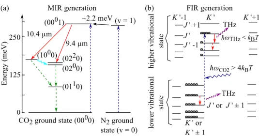
3.1 Optically Pumped Molecular THz Laser
Most of the experiments described in this thesis were carried out on an optically pumped molecular cw THz laser system that is not very commonly used and therefore described in more detail here. It is an effective way of creating THz laser radiation. In this system, molecular gases act as active media for the far-infrared (FIR) radiation and a mid-infrared (MIR) CO
2laser is the source of optically pumping. The following section contains a brief introduction to the physics and characteristics of this monochromatic laser radiation source.
The power of the pump CO
2laser is ≈ 50 W in continuous operation mode and
is achieved with a longitudinal electrical excitation along the resonator. The
electrical excitation populates the first excited state v = 1 of the N
2molecules,
which are inserted in the cavity in addition to the CO
2molecules as shown in
Fig. 3.1(a). The energetic level of the excited N
2and CO
2molecules are similar
and, therefore, due to the collision of both molecules, the energy can be trans-
ferred to the CO
2molecules. The depopulation of this excited state is done by
emitting photons in optical transitions via the 9.4 or the 10.4 µm branch. These
wavelength branches belong to two different optical active transitions between
vibrational modes of the CO
2molecule, see Fig. 3.1 (a). Different wavelengths
can be selected by changing the position of the resonator grating, because the
3 EXPERIMENTAL METHODS 20
Figure 3.1: Scheme of transitions in the MIR and in the FIR gas laser in (a) and (b), respectively. (a) shows the symmetric (10
00), the antisym- metric (00
01) and the bending vibrational modes (02
20), (02
00) and (01
10) of the CO
2molecules. The red arrows indicate the optical laser transi- tions for the wavelengths 10.4 and 9.4 µm. The dashed arrows illustrate the excitation (blue) and the relaxation processes (green). The vertical ar- row indicates the energy transfer between the N
2and CO
2molecules. The buckled cyan arrow is the Fermi resonance. (b) shows the scheme of the transitions in the FIR range in symmetric top molecules, which are pumped by the CO
2energy ~ ω
CO2. The relaxation process happens between the rotational modes within one vibrational state, giving rise to an emission of THz radiation. J and K stand for angular momentum and its projection, respectively (adapted from Ref. [49]).
vibrational modes are rotationally broadened [48, 49]. For a detailed explana- tion and a closer look at the different modes and transitions, see Ref. [49].
The depopulation of the final states of the optical transitions is achieved with
the help of the Fermi resonance and the collision with helium atoms. The out-
put radiation is not used in the experiments, but acts as optical pump source
for the FIR gas laser. The pump laser radiation obtained is now guided to a
zinc selenide (ZnSe) lens with two planar mirrors. The lens focuses the beam
through a polarizing ZnSe Brewster window fixed on a gold-coated steel mirror
with a hole and into the cavity of the FIR laser system, as depicted in Fig. 3.2.
3 EXPERIMENTAL METHODS 21
Figure 3.2: Sketch of the CO
2pump laser generation (MIR) and the optical path to the molecular gas laser with its components. The FIR optical path is illustrated as a red dashed line and the MIR as an orange one (adapted from Ref. [50]).
The strong pump lines of the CO
2laser excite a vibrational state in the molecules of the FIR gas laser system, which have a permanent electric dipole moment as shown in Fig. 3.1 (b). The inserted gas molecules determine the generated wavelength. For this work, methanol (CH
3OH) was used for the wavelength λ = 118.8 µm, corresponding to the frequency f = 2.54 THz, the energy E
~ω= 10.35 meV and the output power P = 90 mW. For pumping this methanol wavelength, the CO
2laser was adjusted to emit the wavelength λ
CO2= 9.695 µm.
Figure 3.1 (b) shows the vibrational states of an optically pumped symmetric
top molecule. J is the angular momentum and K is its projection on the
symmetry axis of the molecule. In the case of the vibrational relaxation being
sufficiently slow, the emission of far-infrared radiation can occur between the
rotational states, as illustrated by the buckled arrows [49]. The dashed arrows
are the relaxation processes and the blue arrow pointing upwards stands for
the optical pumping transition, induced by the CO
2laser energy ~ ω
CO2.
The out coupling window is made out of a silver-coated z-quartz window, which
is transparent for THz frequencies but reflects mid-infrared radiation. There-
fore, the FIR resonator emits monochromatic radiation. The transverse mode
shape of this radiation can be modified by moving the quartz window, resulting
in a change of the resonator length.
3 EXPERIMENTAL METHODS 22
3.2 Microwave Radiation Generation
The high electron mobility transistor (HEMT) samples were also studied with a second wavelength. This wavelength is 3.14 mm, corresponds to a frequency of 95.5 GHz and was generated by a Gunn diode. These diodes are standard radiation sources based on the Gunn effect as discovered by J.B. Gunn [51].
This effect occurs due to the negative differential resistance [52, 53].
The Gunn diode used in this work emits monochromatic radiation with a radiation power of several milliwatts. However, neither the beam profile nor the effective power on the sample surface could be determined to a satisfactory level of accuracy, meaning all of the data obtained by illuminating the sample with the Gunn diode will be given in arbitrary units.
3.3 Variation of Radiation’s Polarization State
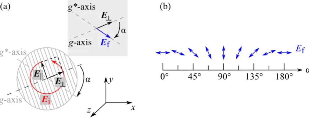
The radiation emitted by the laser system - as described in Chap. 3.1 - is linearly polarized, while the polarization of the Gunn diode is circularly po- larized
1. In this thesis, effects were investigated which are highly sensitive to the polarization states of the radiation. Therefore, it is necessary to be able to control the polarization state, as well as to describe these states theoretically.
The polarization state of the initial electric field vector E
ican be changed by applying a λ/2- or a λ/4-waveplate for the THz range and a wire grid for the microwave radiation. The theoretical description will now be briefly introduced based on the Stokes parameters.
The λ/2- and λ/4-waveplates utilize birefringent medias like, for instance, a x-cut quartz. This quartz includes two different refraction indices n
oand n
eofor the plane ordinary and extraordinary axes, respectively [49]. Both indices are wavelength dependent. The difference of the refraction indices ∆n = n
o− n
eoallows one to fabricate λ/2- or λ/4-waveplates for a selected wavelength.
The electric field vector E
iof the linear polarized radiation, which shines nor- mal to the optical axis c (parallel to the extraordinary axis), can be divided into the parallel and perpendicular electric field vector E
kand E
⊥, respectively.
1
achieved by using the device ”MI-Wave 284 Series Tapered Mode Transitions”, which
transforms a linear polarization to a circular one.
3 EXPERIMENTAL METHODS 23 They are orientated in relation to the c-axis, which is shown in Fig. 3.3(a). Due to this splitting of the electric field and, therefore, the different propagation velocities for those beams inside the media, a phase shift ∆Φ is generated between them. This shift is dependent on the waveplate’s thickness d, the orientation in respect to the optical axis and on the wavelength λ. The shift is given by
∆Φ = n
0d − n
eod = 2πd λ ∆n.
With this equation, it is possible to obtain the thickness d for fabricating wave- plates for the requested wavelength λ. The two important cases for this work are the λ/2-waveplate for rotating the plane of linearly polarized radiation and, secondly, the λ/4-waveplate to obtain circularly (elliptically) polarized radia- tion, see Figs. 3.3 and 3.4, respectively.
For the rotation of the linear polarization a λ/2-waveplate is necessary with a phase shift ∆Φ = (2k + 1)π, where k is numbering the order. In this condition, the linear polarization of the final electric field E
fis rotated by the azimuthal angle α in respect to the initial electric field E
i. The angle α describes the rotation of the polarization and is twice the angle β, which stands for the angle of rotation of the optical axis c as shown in Figs. 3.3(a) and (b). Nevertheless, higher order λ/2-plates are also possible, but result in thicker plates and there- fore in higher absorption of the radiation.
The linear polarization state of the radiation can be described by three Stokes parameters, namely s
0, s
1and s
2[54–57]. Therefore, a coordinate system has to be introduced with the xy-plane lying in the waveplate as shown in Fig. 3.3(a).
To obtain a coincidence with the sample description, the z-axis directs along
the growth direction of the quantum wells and, therefore, against the propaga-
tion direction of the radiation. In this system, the rotation of the final linearly
polarized electric field vector E
fcan be well described by its two components
3 EXPERIMENTAL METHODS 24 E
xand E
y. The rotation can be expressed by the Stokes parameters in the following equations [55, 57]:
s
0= | E
x|
2+ | E
y|
2= I, s
1= | E
x|
2− | E
y|
2s
0= cos(2α), s
2= E
xE
y∗+ E
yE
x∗s
0= sin(2α).
(3.1)
Here, s
0is the polarization independent intensity of the radiation, s
1is the linear polarization within the x- and y-axis and s
2is also the linear polarization, but within a 45
◦rotated coordinate frame of the x- and y-axis.
Figure 3.3: (a) shows a schematic sketch of a λ/2-waveplate with initial polarization state of the incoming radiation E
i. The blue arrow indicates the final polarization state of the radiation E
fon the sample surface. The thickness of the plate is marked by d. (b) illustrates the state of polarization depending on the rotation angle β of the waveplate and on the azimuthal angle α for the rotation of the radiation (adapted from Ref. [50]).
The circular or elliptical polarization can be obtained by using a λ/4-waveplate.
In comparison to the λ/2-waveplate, only the thickness of the material d is dif-
ferent. This can be determined by the phase shift ∆Φ = (2k +
12)π. The
angle ϕ describes the rotation of the c-axis in respect to the direction of E
i,
see Fig. 3.4(a). If ϕ = 45
◦+ k · 180
◦and ϕ = 135
◦+ k · 180
◦then fully right-
handed (σ
+) and left-handed (σ
−) circularly polarized radiation is obtained,
respectively as shown in Fig. 3.4(b). A further notification is that for the ro-
tation of the plate angle ϕ = n · 90
◦the initial polarization of E
iis parallel
3 EXPERIMENTAL METHODS 25
Figure 3.4: (a) shows a schematic sketch of a λ/4-waveplate with linear polarization of the initial electric field E
iand final polarization state of E
f. The thickness of the plate is indicated by d. (b) illustrates the state of polarization, depending on the rotation angle ϕ (adapted from Ref. [50]).
either to the ordinary or to the extraordinary refraction axis. Therefore, the radiation is not influenced by the media concerning its polarization state. Be- tween these angles, the λ/4-waveplate generates elliptical polarization with a maximum at ϕ = 22.5
◦+ k · 90
◦. The polarization states as function of the rotation angle ϕ can be expressed by the four Stokes parameters s
0, s
1, s
2and s
3[54–57]:
s
0= | E
x|
2+ | E
y|
2= I, s
1= | E
x|
2− | E
y|
2s
0= 1 + cos(4ϕ)
2 ,
s
2= E
xE
y∗+ E
yE
x∗s
0= sin(4ϕ)
2 ,
s
3= i(E
xE
y∗− E
yE
x∗) s
0= − P
circ= − sin(2ϕ).
(3.2)
The circular polarization state of the radiation is described by the fourth Stokes parameter s
3. The minus sign in s
3stems from the propagation of the radiation against the z-axis direction.
Both λ-waveplates were used for manipulating the polarization state of the THz
laser radiation. In the case of microwave radiation, a grid polarizer was used to
change the linear polarization of the radiation [49], since no λ-waveplate was
available in this frequency range. Figure 3.5(a) shows a grating with the grating
3 EXPERIMENTAL METHODS 26 axis g, whilst g
∗is the rotated g-axis. The grating axis g is perpendicular to the gate stripes. The initial electric field E
iand the final electric field E
fwith the corresponding polarization state are also depicted. The azimuthal angle α indicates the rotation of the grid, as well as the rotation of the linear polarization. In Fig. 3.5(b), various states of the linear polarization are shown as a function of the angle α.
The principle of the grating is that it is only transparent for the electric field perpendicular to the lattice stripes, meaning parallel to the g-axis, and is non- transparent for the electric field parallel to them (perpendicular to the g-axis).
Therefore, the incoming radiation is disassembled into its two orthogonal parts, E
kand E
⊥. Only the E
⊥part of the radiation is transmitted and follows the rotation of the grating. In the worst case, the incoming linearly polarized radiation will completely vanish. Nevertheless, in this work, the Gunn diode emits circularly polarized radiation and, therefore, nearly the same power at all rotation angles α is obtained due to an equal splitting of the incoming circularly polarized radiation.
Figure 3.5: (a) shows a schematic sketch of a grating with initial circularly
polarized electric field E
iand the final linear polarization state of the electric
field E
fon the sample surface. The grating axis g and the rotated grating
axis g
∗are drawn as dashed grey lines. (b) illustrates the state of linear
polarization depending on the rotation angle α.
3 EXPERIMENTAL METHODS 27
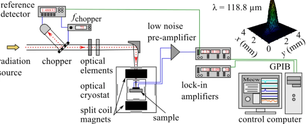
3.4 Experimental Setup
This chapter focuses on the electrical devices, optical elements and the beam path, which are schematically shown in the experimental setup, see Fig. 3.6.
Figure 3.6: A depiction of the optical elements and electrical devices. The radiation path is illustrated as a red dashed line. The devices are named in the picture, but not all connecting wires (blue/ green lines) were drawn from the start of the survey. The top corner shows the beam profile for wavelength λ = 118.8 µm (adapted from Ref. [50]).
The polarized radiation, illustrated as red dashed line in Fig. 3.6, passes through a tilted chopper with a frequency f
chopper= 75 Hz or 625 Hz. The beam is partly reflected into a pyroelectric detector, which is used as a reference detector. This reference signal has two tasks. The first is to stabilize the laser radiation power in the FIR resonator (not shown). The second is to normalize the measured photosignal to the fluctuations of the laser power. The transmitted beam is guided through the optical elements, such as λ/4- , λ/2-waveplates or a grid polarizer. These elements can be rotated stepwise to change the polarization state in a controlled way (see Chap. 3.3). Afterwards, the radiation is focused with a parabolic mirror through the windows of the optical cryostat onto the sample surface. The almost Gaussian beam profile of the THz beam was mea- sured with a pyroelectric camera as shown in the right top corner of Fig. 3.6.
The sample is mounted between two superconducting split coil magnets, al-
lowing the application of magnetic fields of up to ± 7 T perpendicular to the
sample’s surface. In the cryostat, the temperature can be varied between room
3 EXPERIMENTAL METHODS 28 temperature and ≈ 2 K. The photovoltage generated in the sample is amplified with a low noise pre-amplifier and is detected with a standard lock-in amplifier.
The data obtained are processed via the control program, which is based on LabVIEW and records the most important data e.g. the reference signal, the photosignal, the temperature, the magnetic field, etc.
As part of this thesis, experiments with the FIR laser and the Gunn diode were also carried out at room temperature. The setup for the THz laser is the same as for the GHz radiation setup. The Gunn diode has an integrated electri- cal chopper, which consists of a PIN diode controlled by transistor-transistor logic and, thus, makes the optical chopper redundant. The reference signal was obtained by a beam splitting element in the Gunn diode. For the room temperature measurements, the sample was mounted outside the cryostat but electrically connected in the same way as in the low temperature setup.
Figure 3.7: Overview of the used measurement geometries. (a) shows the principle circuit for magneto-transport measurements. An alternating current I
Prewith a frequency f = 12 Hz is applied to the sample. The voltage drop U
xis measured against ground with a lock-in amplifier. The differentially measured voltage U
yin y-direction is not shown. The magnetic field B is applied perpendicularly to the sample surface. In (b) the thinner gate is G1 and the thicker gate is G2. This is illustrated with red and blue fingers, respectively. (c) shows the setup for the photocurrent measurements.
The polarized radiation E
firradiates the sample at normal incidence. The
magnetic field B is applied perpendicularly to the sample surface. For the
photocurrent in (c), both voltage drops | U
x| are measured across a load
resistance R
Lagainst ground. The same can be done for | U
y| in y-direction,
but due to reasons of clarity, this is not shown.
3 EXPERIMENTAL METHODS 29 The measurement geometries used will now be briefly introduced. Figure 3.7(a) shows the magneto-transport geometry. The transport measurements were used for the characterization of the samples, see Chap. 4.1.6. Furthermore, magneto-transport measurements on Hall bar samples of the same batch were carried out by Prof. Tomasz Wojtowicz’s group
2. In the measurements car- ried out in Regensburg, an alternating current I
Preis applied in x-direction of the sample (contacts 1 and 3). The current is in the range of ≈ 50 nA with a frequency of 12 Hz. The voltage drop U
xover the sample is measured and corresponds to the longitudinal resistance of the sample. The Hall voltage U
ycan be measured by connecting contacts 2 and 4 differentially to the lock-in amplifier. These voltages, U
xand U
y, are measured with standard lock-in am- plifiers. Afterwards, the longitudinal and the Hall resistance can be calculated based on R
xx= U
x/I
Preand R
xy= U
y/I
Pre, respectively.
Figure 3.7(b) shows a sketch of the double grating top gate structure, which is fabricated on nearly all sample surfaces used. The thinner gate and the thicker gate stripes are not connected. Therefore, different bias voltages U
G1and U
G2can be applied to the thinner gate G1 and thicker gate G2, respectively. For a detailed description, see Chap. 4.1.2.
Figure 3.7(c) shows the experimental setup for the photovoltage measurement, which is the measurement mainly used in this thesis. The photosignals under investigation are induced by the electric field E
fof the radiation, which irra- diates the sample surface under normal incidence. The polarization states of the electric field can be controllable changed (see Chap. 3.3). For the magnetic quantum ratchet effect, a magnetic field is applied perpendicularly to the sam- ple surface. It is to mention that no voltage, except the dc bias voltage at the gates, is applied to the samples.
The radiation induced photocurrent J
xis detected by a voltage drop U
xof the same values over two similar load resistances R
L. Both voltages are guided to the low noise pre-amplifier, which amplifies differentially. The total photo- voltage is given by U
total= [U
x− ( − U
x)] /2 and is further guided to a lock-in amplifier. In order to obtain the photocurrent J
x, the effective total resistance R
Thas to be calculated. In the experiments, the load resistance R
Lis much
2
Institute of Physics, Polish Academy of Sciences, Al. Lotnikow 32/46 Warsaw, Poland
3 EXPERIMENTAL METHODS 30 smaller than the sample resistance R
S(R
L≪ R
S). Both resistances are parallel connected and therefore, the total resistance R
Tcan be calculated as follows:
R
T= R
L· R
SR
L+ R
Swith R
L≪ R
SR
T≈ R
L· R
SR
S≈ R
L.
(3.3)
Therefore, the voltage drop is directly proportional to the generated photocur- rent and does not feel any extra influence of the sample resistance.
In the calculations, the signal obtained was normalized on the reference signal of the radiation to reduce the influence of the variations of the radiation power.
The reference signal was obtained coincident with the photocurrent signal and
was calibrated with a power measurement before the experiments.
4 Sample Preparation and Characteristics
The magnetic quantum ratchet effect was observed and investigated in CdTe/
CdMgTe and (Cd,Mn)Te/CdMgTe QW samples with a dual grating gate (DGG) superlattice on top of the quantum well structures. Therefore, a brief outline of the wafer growth, the fabrication of the DGG superlattice, the soldering of the ohmic contacts and the characterization of the samples will be given in the following.
Additionally, this thesis also investigates the ratchet effect as detector, which was observed in similar top gate structures as in the MQRE samples, but on high electron mobility transistors. A short overview of the InAlAs/InGaAs/- InAlAs/InP HEMT sample growth, the processing of the superlattice and the sample characteristics will be provided here.
4.1 CdTe and (Cd,Mn)Te Samples
Firstly, the wafer growth of the CdTe and (Cd,Mn)Te samples, which were con- ducted by Prof. Tomasz Wojtowicz’s group will be briefly introduced. As far as the ratchet effects under investigation are concerned, the dual grating top gate superlattice is of importance; hence the processing steps for fabrication will be introduced. These steps involve the design, the electron beam lithogra- phy (EBL), the evaporation of the gate material and the lift-off process of the unnecessary material. All of the methods used in the fabrication of the DGG are standard procedures in semiconductor wafer processing. Therefore, they will be only briefly introduced, as many authors have explained and discussed these methods in detail (refer to, for example, Refs. [58–60] for more details).
The last step in the fabrication of samples is to solder the ohmic contacts. The characterization of the samples is given in the final section.
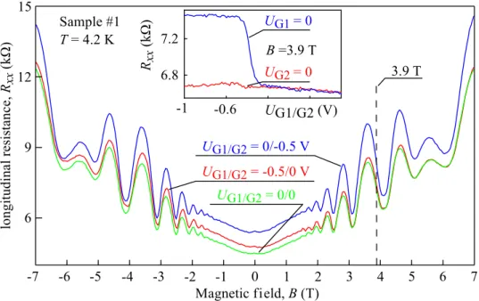
The explanations and methods for the preparation of the DGG will be ex-
plained through the example of (Cd,Mn)Te sample #1, see Tab. 1. All other
CdTe and (Cd,Mn)Te samples, except sample #4, are produced in the same
way. The detailed recipes for each processing step of the superlattice and the
fabrication of the ohmic contacts can be found in the Appendix.
4 SAMPLE PREPARATION AND CHARACTERISTICS 32 4.1.1 Sample Growth
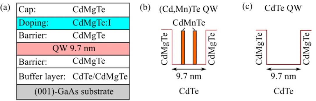
The double grating top gate superlattice is fabricated on (Cd,Mn)Te/CdMgTe and CdTe/CdMgTe single QW structures, which were grown by molecular beam epitaxy on (001)-oriented GaAs substrates [37,47,61–64]. The schematic design of the layer structure and sketches of the QWs can be found in Figs. 4.1(a)- (c), respectively.
A thick buffer layer of 6 µm consisting of CdTe and Cd
0.76Mg
0.24Te layers was grown on top of the (001)-GaAs substrate, followed by a short period of su- perlattices made of CdTe/Cd
0.76Mg
0.24Te as shown in Fig. 4.1(a). These layers were grown to reduce the number of dislocations due to the large lattice mis- match between the GaAs substrate and the Cd
0.76Mg
0.24Te layer. The QW width for both wafers is 9.7 nm and the QW is embedded between two barriers of Cd
0.76Mg
0.24Te alloys. The top side barrier is 10 or 15 nm thick, correspond- ing to (Cd,Mn)Te/CdMgTe or CdTe/CdMgTe QWs, respectively. On top of this barrier, a doped layer was grown, which is 5 nm thick and is composed of CdMgTe:I. In this layer, iodine acts as an electron donor for modulation doping of the 2DEG. To protect the doped region, a cap layer of 50 or 75 nm thickness was grown for either (Cd,Mn)Te/CdMgTe or CdTe/CdMgTe QWs, respectively.
Figures 4.1(b) and (c) illustrate the cross-section of the QWs for (Cd,Mn)Te and CdTe, respectively. The (Cd,Mn)Te/CdMgTe wafer has a single QW con- sisting of (Cd,Mn)Te compound, while CdTe/CdMgTe structures have a non- magnetic CdTe QW. The (Cd,Mn)Te QW has two evenly spaced Cd
0.8Mn
0.2Te layers inserted during the growth process, which are separated by CdTe layers.
The Cd
0.8Mn
0.2Te layers are three monolayers thick and the CdTe layers are eight monolayers thick as shown in Fig. 4.1(b).
In the QW layers of (Cd,Mn)Te, the Cd atoms are exchanged by Mn atoms, which carry a localized spin S = 5/2. This leads to an increase of the effective g
∗-factor of the band carriers and therefore to an enhanced Zeeman splitting
∆E
Zas discussed in Chap. 2.3. For proofing the increased Zeeman splitting
∆E
Z, magneto-photoluminescence studies were performed in a previous work
in which the same wafer material was used, see Ref. [64]. These measurements
show a strong red-shift with increasing magnetic field. From these measure-
4 SAMPLE PREPARATION AND CHARACTERISTICS 33
Figure 4.1: (a) shows a schematic overview of the layer sequences for (Cd,Mn)Te/CdMgTe and CdTe/CdMgTe QWs. The QW is embedded be- tween two barriers of CdMgTe and additionally modulation doped by iodine donors in the doping region on the top side of the wafer. In (b) the sketch of the (Cd,Mn)Te/CdMgTe QW is depicted. The two red bars represent evenly spaced (Cd,Mn)Te layers, which are inserted in the QW between CdTe layers. In (c), the QW for the CdTe wafer is illustrated. Both QWs have the same width of 9.7 nm.
ments, it is possible to extract the average Mn concentration in the digital alloy x = 0.015, as well as the Fermi energy E
F= 1.6 eV from the linewidth.
4.1.2 Structure Design
Before fabricating the dual grating gate superlattice, the layout with the pa- rameters has to be prepared. Therefore, it is necessary to define the location on the sample surface, the width and spacing of the separated gate stripes and their period. A sample with both, a region with a DGG and a region without as reference, is required to compare the photosignals observed that are induced by the DGG and by the untouched surface. Thus, the location of the DGG was fixed at the left side of the sample, as shown in Fig. 4.2(a). The sample sizes vary between 4 × 10 mm
2and 4 × 4 mm
2. In the smaller samples, there is no ungated area large enough to serve as reference.
As discussed in Chap. 2.1, the ratchet effect occurs in asymmetric top gate
structures; therefore, the DGG consists of two different thick gate stripes -
G1 and G2 - which are separated from each other by different distances in
x-direction. The cross-section of the DGG superlattice on top of the QW
4 SAMPLE PREPARATION AND CHARACTERISTICS 34 structure is depicted in Fig. 4.2(b). The source and drain contacts correspond respectively to the points 3 and 1 in Fig. 4.2(a) and are oriented perpendicular to the gate stripes (along the x-axis). The contacts for measuring parallel to the gate stripes (in y-direction) are 2 and 4. The width of the thinner stripes (G1) is d
1= 1.7 or 1.85 µm and the thicker stripes (G2) always have the same width, namely d
2= 3.7 µm (see Tab. 1 and Ref. [37]). To further increase the asymmetry of the superlattice, the spacing between the gate stripes is around a
1= 2.8 µm and a
2= 5.6 µm. Only one structure with ≈ 20% larger spacing, namely a
1= 3.5 µm and a
2= 7.0 µm, was fabricated to clarify the influence of different scaled DGG on the ratchet effect. The asymmetric su- perlattice consists of a repetition of N - between 56 and 65 - times the period d = d
1+ d
2+ a
1+ a
2, see Tab. 1 and Refs. [22,28,37,65]. This results in a total length l, which varies between 875 and 905 µm. The total area covered can be estimated by w
2∗ N d, with w
2as the overlap length of the two different thick gate stripes. The overlap is in the order of 450 − 600 µm as shown in Fig. 4.2(c) and Tab. 1.
The double grating gate stripes consist of 25 or 30 nm thick gold stripes, except sample #4, for which the DGG structure consists of a 75 nm thick dysprosium layer and a 15 nm gold cover layer. The chosen gold stripe thicknesses are al- most transparent for the THz radiation used. This was experimentally proved applying photoconductivity measurements and comparing the photosignals of a free area and an area covered by gold of different thicknesses. For the gold thickness of 25 nm, being relevant for the studied DGG structures, the reduc- tion of the signal was about 10% to 20% whereas for gold of 85 nm thickness, the signal is nearly completely suppressed. Taking into account the skin depth of gold which is in the range of 50 nm for the frequency f = 2.54 THz [66], these measurements demonstrate that the electric field reduction is negligible for the layer thickness smaller than 50 nm which is the case in this thesis.
As outlined, the thinner and thicker gate stripes do not touch each other. To
be able to apply the same voltage to all stripes of G1 or G2, a horizontal gold
stripe interconnects the single stripes; see the sample picture in Fig. 4.2(c).
4 SAMPLE PREPARATION AND CHARACTERISTICS 35
Figure 4.2: (a) shows a sketch of the entire sample with superlattice posi- tion and its gate contacts (red and blue). The ohmic contacts are marked as black squares and numbered from 1-4. The cross-section of the DGG superlattice, which is deposited on top of the QW structure, is shown in (b).
The grating fingers have two different widths, d
1and d
2and are separated by the spacing a
1and a
2. This period d = d
1+ d
2+ a
1+ a
2is repeated N times, resulting in a total length l, see Tab. 1. (c) depicts a photograph of the double grating gate structure and a zoom in to render the gate stripes visible. The thinner stripes, G1, are highlighted with red stripes and the thicker ones, G2, with blue (adapted from [37]).
4.1.3 Electron Beam Lithography and Optical Lithography
The design of the DGG superlattice is transferred to the sample surface by the electron beam lithography or the optical lithography. The superlattice on top of the CdTe and (Cd,Mn)Te QW structures were created by the EBL process, while T. Otsuji’s group
3fabricated the structure by combining the EBL process for the thinner stripes and the optical lithography for the thicker gate stripes for the DGG HEMT samples. Both lithographies are based on the
3
![Figure 2.3: Longitudinal magneto-resistance R xx measured in a Al- Al-GaAs/GaAs heterostructure at temperature T = 8 mK (adapted from [41]).](https://thumb-eu.123doks.com/thumbv2/1library_info/3945741.1534266/16.892.179.714.419.666/figure-longitudinal-magneto-resistance-measured-heterostructure-temperature-adapted.webp)