Clevin Handschin,
1P´ eter Makk,
1,∗Peter Rickhaus,
1Ming-Hao Liu,
2K.
Watanabe,
3T. Taniguchi,
3Klaus Richter,
2and Christian Sch¨ onenberger
11
Department of Physics, University of Basel, Klingelbergstrasse 82, CH-4056 Basel, Switzerland
2
Institut f¨ ur Theoretische Physik, Universit¨ at Regensburg, D-93040 Regensburg, Germany
3
National Institute for Material Science, 1-1 Namiki, Tsukuba, 305-0044, Japan
While Fabry-P´ erot (FP) resonances and Moir´ e superlattices are intensively studied in graphene on hexagonal boron nitride (hBN), the two effects have not been discussed in their coexistence.
Here we investigate the FP oscillations in a ballistic pnp-junctions in the presence and absence of a Moir´ e superlattice. First, we address the effect of the smoothness of the confining potential on the visibility of the FP resonances and carefully map the evolution of the FP cavity size as a function of densities inside and outside the cavity in the absence of a superlattice, when the cavity is bound by regular pn-junctions. Using a sample with a Moir´ e superlattice, we next show that an FP cavity can also be formed by interfaces that mimic a pn-junction, but are defined through a satellite Dirac point due to the superlattice. We carefully analyse the FP resonances, which can provide insight into the band-reconstruction due to the superlattice.
Clean graphene has shown to be an excellent platform to investigate various electron optical experiments, rang- ing from Fabry-P´ erot (FP) resonances [1, 4–6], snake states [3, 8], electron guiding [9], magnetic focusing [10, 11], Veselago lensing or angle-dependent transmis- sion studies of negative refraction [12, 13]. The pn - junctions are basic building blocks of many of these ex- periments, which for example are used to confine elec- trons into FP cavities, where the pn-junctions play the role of semireflective mirrors. The study of FP resonances have already revealed themselves as a powerful tool to in- vestigate various aspects of graphene. Examples are the π-shift of the FP resonances at low magnetic field origi- nating from Klein tunnelling [26] in single layer graphene [1, 2, 7] or the FP resonances in ultraclean, suspended de- vices that proved ballistic transport over several microns [4, 5].
Encapsulation of graphene in hexagonal boron nitride (hBN) [18] can not only allow for quasi-ballistic transport (the mean free path is comparable or larger than the de- vice geometry), but can also be used for the creation of a superlattice in graphene due to the periodic potential modulation of the Moir´ e pattern. Such a pattern stems from a small lattice mismtach of graphene and hBN. The modified bandstructure of graphene, which includes the emergence of satellite Dirac peaks (satellite DPs), is ex- perimentally observable only for small misalignment an- gles (θ) between hBN and graphene [19]. The formation of a Moir´ e superlattice has been demonstrated in various spectroscopy [19, 22, 30] and transport [11, 12, 16, 23, 26–
30] experiments. Besides experiments, considerable ef- fort has been invested to calculate the band-structure of graphene under the influence of such a Moir´ e superlattice [29, 33, 34].
Here we demonstrate confinement using band engineer- ing based on locally gated Moir´ e superlattices and the appearance of FP resonances defined by the main and satellite DPs playing the role of reflective barriers. Al-
though several aspects of FP cavities have been investi- gated, such as the effect of the pn-junction smoothness on the visibility of the FP resonances [4], the electronic tunability of the cavity size has not been studied. First, we will discuss samples with a large misalignment angle between the hBN and graphene. We find that the cav- ity size is strongly dependent on carrier density in and outside the cavity. Then, we turn to aligned samples with a superlattice structure and take advantage of the large tunability of the cavity size to obtain additional in- formation on the modulated Moir´ e band-structure which is yet not fully understood. Our findings are consistent with the electron-hole symmetry breaking of the Moir´ e superlattice [29].
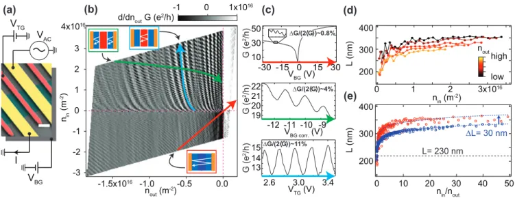
The device geometry of our two-terminal pnp-junction is shown in Fig. 1a: a global back-gate and a local top-gate is used to separately control the charge car- rier density in the inner (n
in) and outer (n
out) regions thus forming pp’p- or pnp-junctions. In order to re- duce the cross-talk between the gates we used a thin (∼ 30 nm) hBN layer. Therefore n
outcan be calculated according to n
out= V
BG· (1/C
SiO2+ 1/C
hBN,b)
−1, where C
SiO2and C
hBN,bare the geometrical capacitances of the SiO
2and bottom hBN respectively, and V
BGand V
TGthe applied gate-voltages. In analogy, n
inis given by n
in= V
BG· (1/C
SiO2+ 1/C
hBN,b)
−1+ V
TG· C
hBN,twhere C
hBN,tis the top hBN capacitance. The Cr/Au contacts dope the graphene in its proximity n-type, independent of V
BG. The conductance is measured in a two-terminal configuration as a function of V
BGand V
TG(which can be directly converted to n
inand n
out), as shown in Fig. 1b.
The overall device length is roughly 1 µ m, with a top- gate width of 230 nm being centered in the middle of the device. In the measured device, a high mobility of the electrons and holes (µ
e,h) was extracted from field effect measurements, yielding µ
e∼ 150 000 cm
2V
−1s
−1and µ
h∼ 50 000 cm
2V
−1s
−1respectively.
All structures were fabricated following the procedure
arXiv:1701.09141v1 [cond-mat.mes-hall] 31 Jan 2017
V
TGI V
BGV
AC1514
2G (e/h)13 3
2 1 0 -1 -2 -3 4x10¹⁶
nout (m-2) nin (m-2)
-1 0 1x10¹⁶ d/dnout G (e2/h)
-1.5x10¹⁶ -1.0 -0.5 0.0 2221
2G (e/h)20 19 50 30
2G (e/h)10
(b)
(a) (c) (d)
∆G/(2 G )~0.8%
∆G/(2 G )~4%
∆G/(2 G )~11%
3.4 3.0 2.6 VTG (V)
-12 -11 -10 -9 VBG corr. (V) -30 -15VBG0 (V)15 30
nin/nout 10
0 20
200 300 400
L (nm)
30 40 50
∆L= 30 nm nin (m-2) 3x10¹⁶ 1
0 2
200 300 400
L (nm)
nout
low high
(e)
L= 230 nm
FIG. 1. Fabry-P´ erot resonances measured in a two-terminal pnp-configuration. a, False-color SEM image with the measurement configuration sketched. The contacts are shown in yellow, the top-gate in red and the graphene between the two hBN-layers is shown in cyan. Scale-bar equals 500 nm. b, Numerical derivative of the conductance as a function of global back-gate (V
BG) and local top-gate (V
TG). Here it is replotted as a function of charge-carrier density in the outer (n
out) and inner cavity (n
in). The three most important FP resonances present in the system are indicated. c, Visibilty ∆G/ h2Gi of the FP resonances indicated in (b) in comparison. d, Extracted cavity length of the central cavity as a function of n
in, as indicated with the cyan arrow in (b), for different values of n
out. e, The same data as shown in (d), but now plotted as a function of n
in/n
outfor experiment (red) and theory (blue, for transport simulation see Supporting Information). The black, dashed line corresponds to the width of the top-gate measured with the SEM. The blue, dashed lines are a guide to the eye for the theoretical data and the theoretical data shifted by 30 nm respectively.
given by Wang et al. [15] with some additional improve- ments. A detailed description of the fabrication is given in the Supporting Information. The measurements were done using low frequency lock-in technique in a vari- able temperature insert (VTI) with a base-temperature around T = 1.6 K.
The derivative of the differential conductance with re- spect to n
inand n
outare shown in Fig. 1b for n
out< 0.
The visible fringes are FP resonances appearing in the pp’p regime (bottom part, n
in< 0) and pnp regime (up- per part, n
in> 0). Specific cuts within an extended (red) or limited (blue, green) gate-range are shown in Fig. 1c.
While the FP resonances in the inner (outer) cavities are tuned predominantly by n
in(n
out) as indicated with the blue (green) arrow in Fig. 1b, the FP resonances between the contacts depends on both densities as indicated by the red arrow. The three types of FP resonances are very different in their visibility ∆G/(2 hGi). Here ∆G is the difference between the conductance at constructive and destructive interference, and hGi denotes the mean conduction in between oscillation maximum and mini- mum. The FP resonances between the contacts yield the lowest visibility (∼ 1%), those in the outer cavi- ties yield an intermediate visibility (∼ 4%) and FP res- onances in the inner cavity yield the highest visibility (∼ 11%). In ballistic graphene, the FP visibilities depend on the transmission/reflection properties of the confin- ing boundaries, namely the pn-interface. The transmis-
sion/reflection probabilities of a pn-interface strongly de- pends on the angle of the incoming charge carrier [28]. In the case of a “sharp” pn-junctions (d λ
F, where d de- notes the distance over which the density changes and λ
Fis the Fermi wavelength), transmission of charge carriers is possible up to large angles measured with respect to the pn-junction normal. In contrast, for a very “smooth”
pn-junction (d λ
F), only charge carriers at low angles are transmitted (in our device this is around ∼ 20
◦, al- though depends strongly on the gate voltages). Since our conductance measurement is not angle resolved, the mea- sured signal averages over all possible angles and leads to smearing of the FP resonances. It turns out that for a smooth pn-junction, which transmits a narrower range of angles, the highest FP visibilities can be observed [4].
In our system we discriminate between two types of pn- junctions: i) the pn-junction created in proximity of the contacts for n
out< 0 and ii) the pn-junction created us- ing the global back-gate and local top-gate. We note that (ii) is much smoother compared to (i) (see Supporting In- formation). Following the above given argument one sees that the FP resonance visibility is highest/lowest when the cavity is defined by two softer/sharper pn -junctions.
We will now extract the effective cavity length, L from
the FP oscillations in the central cavity, which deviates in
most cases from the physical width of the top-gate. As-
suming a FP resonator with a hard-wall potential (fixed
width of the cavity), the cavity width can be extracted
from the FP oscillations. Constructive interference forms if the path-difference between directly transmitted and twice reflected waves is equal to 2L = jλ
F, where λ
Fis the Fermi wavelength and j is an integer. The j-th FP resonance can be rewritten as L √
n
j= j √ π using λ
F= 2π/k
F= 2 p
π/n which is valid for single layer graphene. For two neighboring peaks, for example j-th peak at density n
jand (j + 1)-th peak at density n
j+1:
L =
√ π
√ n
j+1− √
n
j. (1)
We note here that in Equation 1 L is independent of n
outwhich is an oversimplification of the problem. An alternative way to define the cavity length is to mea- sure the distance between the two zero-density points of the right and left pn-junctions. However, since the po- sition of the pn -interface is experimentally not directly accessible we will use Equation 1 to deduce the cavity size. More discussion on this is given in the Supporting Information. The cavity length was extracted by taking various linecuts comparable to the one indicated with the blue arrow in Fig. 1b and then using Equation 1. We ob- serve an increase of L with increasing n
in(for fixed n
out), and a decrease of L with increasing n
out(for fixed n
in) as shown in Fig. 1d. Consequently L does depend on n
out, as expected. Surprisingly, by plotting L as a func- tion of n
in/n
out, all data-points lie on one universal curve which is shown in Fig. 1e, independent of the exact posi- tion within Fig. 1b from which they have been extracted from. Within the applied gate-range, L varies substan- tially, by up to 200 nm, which corresponds to a shift of around 100 nm per pn-junction. The evolution of L as a function of n
in/n
outextracted from the experiment was compared with the one extracted from a transport simu- lation (based on the method described in Ref. [4]) using Equation 1. The latter reveals good qualitative agree- ment with the experiment as shown in Fig. 1e. The most significant difference between experiment and theory are:
i) an off-set of ∆L ∼ 30 nm from the theory to the ex- periment and ii) a disagreement between the trends of the two curves when approaching very low charge car- rier densities in the outer cavity, corresponding to large values of n
in/n
out(the same is true when depleting the inner cavity, not shown here). In the experiment the cav- ity length L saturates while it increases continuously in the theory. We believe that the reason for this is that the measured sample bears a residual doping (n
∗) which is not present in theory. The residual doping causes that for values below n
∗the electrostatic gates are unable to further deplete the graphene, thus for V
BG→ 0 the ef- fective value of n
in/n
out(tuning L) remains fixed. The off-set of the two curves (i) might origin from a too nar- row top-gate in theory if the top-gate in the experiment was measured with an error of ∼ 30 nm.
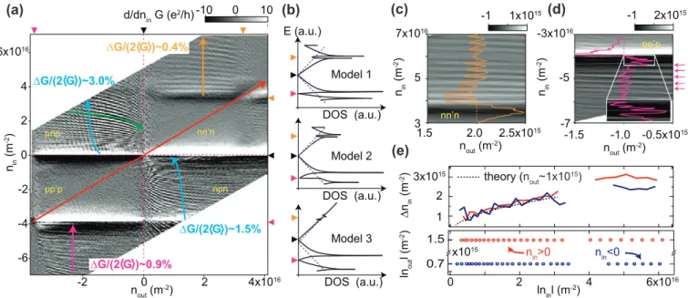
Now we turn to graphene which is aligned with a small twist angle with respect to one of the hBN layers. The resulting band-reconstruction includes additional satel- lite DPs which are indicated with the purple and orange triangles in Fig. 2a where the derivative of the conduc- tance is plotted. The main DP is indicated with the black triangle. At low doping the semitransparent boundaries in the bipolar region are defined by the main DP (com- parable to Fig. 1b) and FP resonances within inner and outer cavity are observed, marked by the green and cyan arrows, respectively.
Whereas in Fig. 1b,c the contacts are the only bound- aries leading to FP resonances in the unipolar regime (red arrow), additional semitransparent boundaries, formed by the satellite DPs, emerge at high doping in the pres- ence of a superlattice. As a result, novel FP oscillation are visible at high doping as indicated with the purple and orange arrows in Fig. 2a, which are absent in Fig. 1b (no Moir´ e superlattice). This new set of FP oscillation re- sembles again the pattern known from the bipolar regime and the transition from FP resonances across the whole sample to FP resonances within the inner and outer cav- ity is a direct consequence of the satellite DPs forming these additional semitransparent boundaries. There are also charge carriers that bounce between the contacts and the satellite DP boundary, leading to weak resonances as a function of n
out(see Supporting Information).
In the following, we compare the visibility be- tween FP resonances across the main DP and the satellite DP within the inner cavity for n
in> 0 and n
in< 0 separately (µ
e∼ 100 000 cm
2V
−1s
−1, µ
h∼ 50 000 cm
2V
−1s
−1. Charge carriers for n
in< 0 (hole side) bouncing between boundaries formed by the satellite DPs (∆G ∼ 0.9%) show a visibility that is 40% lower than the visibility of the main DP oscilla- tion (∆G ∼ 1.5%), as shown in Fig. 2a. In contrast, for n
in> 0 (electron side), the visibility is reduced by 85%
(∆G ∼ 0.4% at the satellite DP compared to ∆G ∼ 3%
at the main DP). To interpret these observations, we con- sider a family of possible Moir´ e minibands for graphene on hBN substrate, which was calculated by Wallbank et al. [29] using a general symmetry-based approach. Be- cause the relatively large number of model-dependent pa- rameters of the symmetry breaking potential can strongly influence the obtained Moir´ e perturbation, the focus was on the generic features for different sets of parameters used. In Fig. 2b, the DOS for three different sets of pa- rameters are plotted. Details on the parameters can be found in Ref. [29].
For the case of n
in< 0, when crossing the satellite DP on the hole side, the DOS between inner and outer cavity decreases to zero (independent of the parameters used for the calculations of the DOS as given in Ref. [29]) for all k
x,y, as indicated with the purple triangle in Fig. 2b.
This result is experimentally supported by capacitance
spectroscopy of hBN-graphene-hBN heterostructures in
d/dnin G (e2/h) -10 0 10
nout (m-2) 2 4x10¹⁶
-2 0
nin (m-2) 6x10¹⁶
4 2 0 -2
-6 -4
(a)
(e)
-5 -7 -3x10¹⁶
nout (m-2) nin (m-2)
-1 2x10¹⁵
-0.5x10¹⁵ -1.5 -1.0
pp’p
(d)
5 3 7x10¹⁶
nout (m-2) nin (m-2)
2.5x10¹⁵
1.5 2.0
nn’n
-1 1x10¹⁵
DOS (a.u.) E (a.u.)
Model 1
DOS (a.u.) Model 2
DOS (a.u.) Model 3
(b)
pp’p pnp nn’n
npn
∆G/(2 G )~0.9%
∆G/(2 G )~1.5%
∆G/(2 G )~0.4%
∆G/(2 G )~3.0%
(c)
0.7 1.5
lninl (m-2) 6x10¹⁶ 2
0 4
2
-2∆n (m) 3x10in 115
lnoutl (m-2)
x1015 nin>0 nin<0
theory (nout~1x10¹⁵)
FIG. 2. Fabry-P´ erot resonancesin in the presence of a Moir´ e superlattice. a, Numerical derivative of the conductance as a function of n
inand n
out. The red, cyan and green lines indicate the regular FP resonances described in Fig. 1. Additional FP resonances emerge if n
inor n
outis tuned above or below a satellite Dirac peak. These FP resonances are indicated with orange and purple arrows. The position of the main and satellite DPs are indicated with black and purple/orange triangles respectively. b, DOS of graphene as a function of energy in the presence of a Moir´ e superlattice with hBN for three different parameter sets used in the calculation performed by Wallbank et al. Figure adapted from Ref. [29]. Black, orange and purple triangles indicate main and satellite Dirac-peaks respectively. The blue, dashed line indicates the DOS for unperturbed graphene. c,d, High-resolution measurements (d/dn
inG (e
2/h)) of the regions where the inner cavity is tuned beyond the satellite DP and the additional FP resonances are present. e, Position of the individual FP resonance peaks (lower panel) and their relative spacing ∆n
in(upper panel) is plotted as a function of n
in. The black, dashed line indicates the values expected from theory. If the semitransparent boundaries are defined via the satellite DP the spacing is further increased. However, no precise trend of ∆n
in(increasing or decreasing) as a function of n
incan be seen from the few data-points extracted.
the presence of a Moir´ e superlattice [30]. The vanishing DOS leads to similar reflection/transmission coefficients as for the main DP, resulting in a comparable visibility of the two FP resonances. A representative cut at fixed n
out< 0 is shown in Fig. 2d.
For the electron side with n
in> 0, the significantly re- duced visibility is in qualitative agreement with the band- structures shown in Fig. 2b, since the DOS at the satellite DP (indicated with an orange triangle) is reduced (de- pending on the parameters used in the calculation), but never vanishes. A representative cut at fixed n
out> 0 is shown in Fig. 2c. A direct implication of the finite DOS is that only some charge-carriers have a nonzero reflec- tion coefficient, thus contributing to the FP resonances, while the remaining ones account for a background cur- rent. It is worth noting, that even though the visibility of the FP resonances across the electron side satellite DP (n
in,out> 0, Fig. 2c) are significantly reduced, they seem to be more regular over a wider gate-range com- pared to the FP resonances across the hole satellite DP (n
in,out< 0, Fig. 2d). However, this could be as well just sample-specific since the mobility in the hole side was significantly lower compared to the electron side.
We now compare the evolution of the position of the
individual FP resonance peaks (|n
out| ∼ const.) and their relative spacing ∆n
inas a function of n
in, which are plot- ted in the lower and upper panel of Fig. 2e. The latter analysis is performed instead of the cavity length analy- sis since Equation 1 does not hold any more if the Fermi- energy is tuned beyond the satellite DP. This is because in Equation 1 a circular Fermi-surface and electron like dispersion is assumed, which does not hold in the pres- ence of a strong band-modulation. In contrast, mapping the FP resonance peak position as a function of charge- carrier density is free of any assumptions and therefore independent of the band-structure. If the semitranspar- ent interfaces are defined via the main DP, the evolution of ∆n
inbetween neighboring peaks as a function of n
inis in good agreement with the values extracted from theory (transport simulation in the absence of a Moir´ e super- lattice), which is indicated with the black, dashed line in Fig. 2e. If the semitransparent interfaces are defined via the satellite DPs, the density-spacing between the FP resonance peaks is further increased on both, the electron and hole side.
Although a precise extraction of the cavity size is not possible with Equation 1, an estimate can still be given.
We have found a cavity size of L∼ 250 nm to 310 nm on
the electron side if the density is measured from the main DP, whereas setting the density to zero at the satellite DP gives an unphysical cavity size (L∼ 80 nm to 200 nm).
On the electron side the density of states seems almost unaltered, as can be seen in Fig. 2b, however the band- structure is substantially modified, which can be seen in Ref. [29]. The band-structure consists of two non- isotropic bands above the satellite DPs which makes the situation rather complex, with different visibilities and angle dependent transmissions for the two bands. On the hole side the cavity size analysis yields cavity sizes of L∼ 280 nm to 360 nm if the density is measured from the main DP. At the satellite DP the density of states decreases to zero, meaning that a real Dirac point is formed. Therefore one might expect, that the density for the FP oscillations should be measured from the satel- lite DP. However by setting the charge-carrier density to zero at the hole satellite DP, the analysis gives un- physical results. We note, that close to the hole satellite DP Equation 1 should be valid if counting the charge- carrier density from the satellite DP, since the band- structure is isotropic. Besides the most pronounced FP resonances indicated with the purple arrow in Fig. 2d, a second set of resonances with a much shorter period seem to appear in the very vicinity of the hole satel- lite DP (see inset of Fig. 2d). For these resonances the extracted cavity length leads only to reasonable values (L∼ 300 nm) when counting the charge carrier density starting from the satellite DP. Unfortunately the resid- ual doping (n
res∼ 0.4 × 10
15m
−2to 1 × 10
15m
−2) pre- vents us from resolving more of these features in the very vicinity of the satellite DP. A possible explanation for the different behavior of the two sets of FP oscillation (n
out< 0) might be the following: The small resonances are only observed up to densities of ∆n< 2 × 10
15m
−2(where ∆n is measured from the satellite DP), where the Moir´ e miniband remains close to Dirac like (linear disper- sion relation). The Fermi energy corresponding to theses small oscillations is consequently exclusively tuned in the linear part of the Moir´ e miniband (see Supporting Infor- mation). From the band-structures we would expect that the small oscillations should be visible up to higher dop- ing values, namely values which are larger by a factor of up to ∼ 10 depending on the model. This estimate is based on the energy-spacing between the satellite DP and the first van Hove singularity at higher energies, ex- tracted from theory (see Supporting Information). Note that the extracted energy-spacing corresponds to an up- per bound within which the dispersion relation might be considered as linear. The Fermi energy corresponding to the stronger resonances indicated with the purple ar- row, does partially reside outside of the linear region of the Dirac cones where the band-structure becomes more complex, including singularities and band-overlaps.
We note that in the work of Lee et al. [16] they sug- gest that model 3, which is shown in Fig. 2b, is the one
describing the experimental situation best. Furthermore, for model 1, where multiple satellite DPs appear near ev- ery main DP, Equation 1 would also have to be multiplied by a factor of √
g
SDP, where g
SDPis the additional degen- eracy of the satellite Dirac cones. Although by including additional degeneracies, and counting the density from the satellite DP, the strong oscillations could give rea- sonable cavity sizes, however, for the small oscillations, the additional degeneracies would result in too large cav- ity sizes. Moreover, most experimental evidence points to a single Dirac cone at the satellite DP. We also note here, that the visibility of these resonances are quite low, which could also introduce some experimental error in the analysis.
In conclusion, we first analysed a pnp-junction in the absence of a Moir´ e superlattice where the varying visi- bility of the different types of FP resonances could be linked to sharp and smooth pn-junctions in the system.
Furthermore, the change of the effective cavity length depending on n
inand n
outcould be mapped via the FP resonances. In a second sample, the presence of a Moir´ e superlattice gave rise to satellite DPs and the modified band-structure resulted in confinement of electronic tra- jectories and in the appearance of FP resonances. Al- though the oscillations are formed in the Moir´ e mini- bands, they can mostly be described as if they would originate from the non-modified band-structures. Fur- ther studies will be needed to explain these findings.
Our results show that confinement of electrons can be obtained using miniband engineering. Future studies can investigate the angle dependent transmission properties of such an interface. Moreover combining the studies of transverse magnetic focusing [16] and bias spectroscopy studies of FP resonances or detailed studies of the magnetic field dependence of FP resonances can reveal further details on the band reconstruction.
ACKNOWLEDGMENTS
This work was funded by the Swiss National Science Foundation, the Swiss Nanoscience Institute, the Swiss NCCR QSIT, the ERC Advanced Investigator Grant QUEST, and the EU flagship project graphene. M.-H.L.
and K.R. acknowledge financial support by the Deutsche Forschungsgemeinschaft (SFB 689). The authors thank John Wallbank, David Goldhaber-Gordon, Simon Zihlmann and L´ aszlo Oroszl´ any for fruitful discussions.
∗
Peter.Makk@unibas.ch
[1] L. Campos et al., Nat Commun 3, 1239 (2012).
[2] A. L. Grushina, D.-K. Ki, and A. F. Morpurgo, Appl.
Phys. Lett. 102, 223102 (2013).
[3] P. Rickhaus et al., Nat Commun 4, 2342 (2013).
[4] A. Varlet et al., Phys. Rev. Lett. 113, 116601 (2014).
[5] M. Ben Shalom et al., Nat Phys 12, 318 (2016).
[6] E. V. Calado et al., Nat Nano 10, 761 (2015).
[7] P. Rickhaus et al., Nat Commun 6, 6470 (2015).
[8] T. Taychatanapat et al., Nat Commun 6, 6093 (2015).
[9] P. Rickhaus et al., Nano Lett. 15, 5819 (2015).
[10] T. Taychatanapat, K. Watanabe, T. Taniguchi, and P. Jarillo-Herrero, Nat Phys 9, 225 (2013).
[11] V. E. Calado et al., Applied Physics Letters 104, 023103 (2014).
[12] G.-H. Lee, G.-H. Park, and H.-J. Lee, Nat Phys 11, 925 (2015).
[13] S. Chen et al., Electron optics with ballistic graphene junctions, arXiv:1602.08182.
[14] O. Klein, Z. Phys. 53, 157 (1929).
[15] A. V. Shytov, M. S. Rudner, and L. S. Levitov, Phys.
Rev. Lett. 101, 156804 (2008).
[16] A. F. Young and P. Kim, Nat Phys 5, 222 (2009).
[17] A. Varlet et al., Phys. Status Solidi RRL 10, 46 (2016).
[18] C. R. Dean et al., Nat Nano 5, 722 (2010).
[19] C. R. Woods et al., Nat Phys 10, 451 (2014).
[20] M. Yankowitz et al., Nat Phys 8, 382 (2012).
[21] G. L. Yu et al., Nat Phys 10, 525 (2014).
[22] Z. Shi et al., Nat Phys 10, 743 (2014).
[23] B. Hunt et al., Science 340, 1427 (2013).
[24] L. A. Ponomarenko et al., Nature 497, 594 (2013).
[25] C. R. Dean et al., Nature 497, 598 (2013).
[26] R. V. Gorbachev et al., Science 346, 448 (2014).
[27] L. Wang et al., Science 350, 1231 (2015).
[28] P. Wang et al., Nano Lett. 15, 6395 (2015).
[29] M. T. Greenaway et al., Nat Phys 11, 1057 (2015).
[30] C. Kumar, M. Kuiri, J. Jung, T. Das, and A. Das, Nano Lett. , (2016).
[31] M. Lee et al., Science 353, 1526 (2016).
[32] J. R. Wallbank, A. A. Patel, M. Mucha-Kruczynski, A. K. Geim, and V. I. Fal’ko, Phys. Rev. B 87, 245408 (2013).
[33] P. Moon and M. Koshino, Phys. Rev. B 90, 155406 (2014).
[34] J. R. Wallbank, M. Mucha-Kruczynski, X. Chen, and V. I. Fal’ko, ANNALEN DER PHYSIK 527, 359 (2015).
[35] L. Wang et al., Science 342, 614 (2013).
[36] V. V. Cheianov and V. I. Fal’ko, Phys. Rev. B 74, 041403
(2006).
SUPPORTING INFORMATION Low magnetic field measurements
5.6
5.6 -5 5.6
-7 VTG (V)
-5
-7 VTG (V)
-5
-7 VTG (V)
0
-500 500
B (mT)
0
-500 B (mT) 500
0
-500 B (mT) 500 d/dVTG G0
G0 (e2/h) 20.0 23.5
-3 2
-0.2 0.2
∆Gosc (e2/h)
(b)
-3.0
-4.2 VTG (V)
-3.0
-4.2 VTG (V)
-3.0
-4.2 VTG (V)
0
-500 B (mT) 500
0
-500 B (mT) 500
0
-500 500
B (mT) G0 (e2/h) 21.5 23.5
d/dVTG G0 -6 6
-0.2 0.2
∆Gosc (e2/h)
(c)
3.4
2.6 VTG corr. (V)
3.4
2.6 VTG corr. (V)
3.4
2.6 VTG corr. (V)
V (V)TG corr.5 7
4.0 VTG corr. (V)
4.0 VTG corr. (V)
4.0 VTG corr. (V) -100 0 100
B (mT) -500 0 500
B (mT) -500 0 500
B (mT)
-100 0 100
B (mT) -500 B (mT)0 500 -500 0 500
B (mT)
-100 0 100
B (mT) -500 B (mT)0 500 -500 0 500
B (mT) G0 (e2/h)8 14
d/dVTG corr.G0-20 20
∆Gosc (e2/h)-0.8 0.8
G0 (e2/h) 31.9 32.3
d/dVTG corr.G0-0.4 0.4
-0.025 0.025
∆Gosc (e2/h)
G0 (e2/h) 42.5 43.0
d/dVTG corr.G0-0.3 0.6
-0.04 0.04
∆Gosc (e2/h)
(a) (d) (e)
V (V)TG corr.5 7
V (V)TG corr.5 7
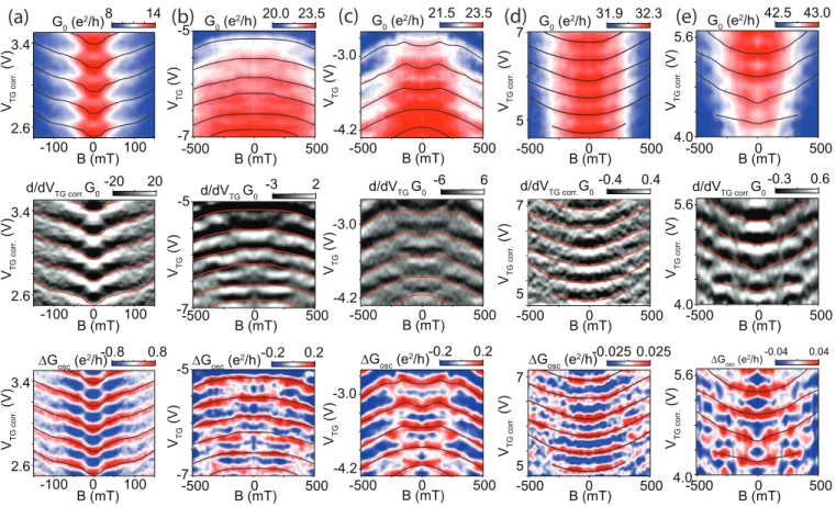
FIG. S1. Low magnetic field measurements of the FP resonances across the main and satellite DPs. First row is the net conductance, second row the numerical derivative along the gate-axis and third row the net conductance oscillation.
Columns (a) is the measurements across the main DP with n
in> 0 and n
out∼ −0.3 ·10
16m
−2, column (b,c) are measurements across the satellite DP with n
in< 0 where n
out∼ −0.7 · 10
16m
−2and n
out∼ −2.8 · 10
16m
−2, column (d,e) are measurements across the satellite DP with n
in> 0 where n
out∼ 2.1 · 10
16m
−2and n
out∼ 2.8 · 10
16m
−2.
Fabry-Perot (FP) resonances disperse towards higher doping (k values) with increasing magnetic field [1–6] as seen in Fig. S1a-c. This results from the resonance condition ∆θ
WKB+ Φ
AB= const. where ∆θ
WKBis the Wentzel- Kramers-Brillouin phase acquired on the path of the charge-carriers trajectory, and Φ
ABis the Aharonov Bohm phase [3, 7].
Furthermore one can determine the Berry’s phase acquired by a charge carrier encircling the origin in k-space. For single layer graphene with a staggered sublattice potential, which breaks its inversion symmetry [8], the Berry’s phase becomes exactly π as the gap approaches zero [9]. This has been observed experimentally in FP measurements [1]
and quantum Hall measurements [10]. In Fig. S1 we show low magnetic field measurements for FP oscillations across
the main DP (a) and the satellite DP in the hole (b,c) and electron (d,e) doped region. Each of the measurements
was plotted in three different ways showing the net conductance, the numerical derivative of the net condctance
and the net oscillation. The black/red lines in Fig. S1 were extracted numerically and track the peak-position of
the FP oscillations with magnetic field. For the FP resonances across the main DP we see the π-shift at roughly
B = 30 − 50 mT as shown in Fig. S1a. Following the previously given argument, one might expected as well a π-shift
for the FP resonances across the satellite DP on the hole side, since there the DOS drops to zero comparable to the
main DP. However, measurments at different n
out, shown in Fig. S1b,c, did not allow a conclusive statement whether
such a π-shift is present or not. It seems however that for both of the here preseneted situations an intriguing pattern
appears at low magnetic fields (i.e. B < 200 mT). At higher field, the FP oscillations disperse constantly. On the
electron side, i.e. n
in> 0, the situation is less clear. The pattern in the middle exhibits less strong variations.
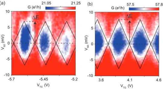
Bias-spectroscopy of Fabry-P´ erot resonances
(a)
-10 -5 0 5 10
4.6 4.1
3.6
G (e2/h) 57.5 57.8
VTG (V) VSD (mV)
-10 -5 0 5 10
-5.2 -5.7
G (e2/h)
VTG (V) VSD (mV)
(b)
∆E
-5.45
21.05 21.25
∆E
FIG. S2. Bias spectroscopy on FP resonances a, Measurement of FP resonances across the main DP (n
in< 0, n
out> 0) where an energy spacing corresponding to L = 300 nm is indicated. b, Comparable measurement for the satellite DP with n
in, n
out> 0. Energy spacing corresponds to L = 280 nm.
Bias spectroscopy of the FP resonances can be used as an alternative way to extract the cavity length. The resonance condition in a cavity is given by L = j · λ/2, or k
F= jπ/L, where j is an integer. For single-layer graphene in the absence of a Moir´ e superlattice, the energy spacing ∆E between two consecutive FP resonances is equidistant and given by
∆E = ~ v
F[(j + 1) − j] π L = ~ v
Fπ
L (2)
where ~ is the reduced Planck constant and v
F∼ 10
6m/s is the Fermi velocity. The size of the diamond corresponds to twice the level spacing, 2∆E, leading to:
L = ~ v
Fπ
∆E . (3)
The measurement of the bias spectroscopy across the main DP is in qualitative agreement with the extracted cavity
length using Equation (4). In Fig. S2a, an energy spacing corresponding to L ∼ 300 nm according to Equation (3)
is indicated. Similar results are found for the FP resonances across the satellite DP with n
in> 0, shown in Fig. S2b
where an energy spacing corresponding to L = 280 nm is indicated in the plot. Note that Equation (3) is based on
the energy-dispersion of unperturbed graphene, neglecting a modification of the band structure in the presence of a
Moir´ e superlattice. On the hole side, the pattern was too complex to extract any reasonable information.
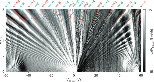
Quantum Hall Measurements
d/dVBG corr. G (e2/h)
0 2 4
-60 -40 -20 0 20 40 60
VBG corr. (V)
B (T)
6
-15 8 ν=-2 ν=-18ν=2 ν=-14ν=6 ν=-10ν=10 ν=-6 ν=14ν=-2ν=-18ν=18ν=2ν=-14 ν=6ν=-10 ν=10 ν=-6 ν=14ν=-2 ν=18 15
FIG. S3. Quantum Hall measurement in high magnetic field. Numerical derivative of the conductance as a function of the global back-gate and magnetic field reveals the expected filling-factors emerging at the main DP (red) and at the satellite DPs (cyan and green) as observed in Ref. [11, 12]
Measurement of the quantum Hall Effect in the unipolar regime reveals the emergence of the filling-factors associated with graphene from the main DP and the two satellite DPs, and similar results have been reported in Ref. [11, 12].
Thermal annealing of hBN-graphene-hBN heterostructures
(a) (b)
G (e2/h)20 40-30 -20 -10
VBG (V) 40 30
G (e2/h)20
-30 -20 -10
VBG (V) 30 40
G (e2/h)20 5
4
2
0-30 -20 -10
VTG (V) 3
1
VBG (V) 30
29 28 27 4.8 4.6 4.4 4.2 4.0 3.8 3.6 3.4 VTG corr. (V)
G (e2/h)
(c) (d)
FIG. S4. Self-cleaning properties of hBN-graphene-hBN heterostructures upon thermal annealing. a, Conduction map with FP resonances clearly visible in the bipolar region. b, Same map after degradation of the sample where the FP resonances are nearly absent. c, Most of the FP resonances are restored after thermal annealing at 200
◦C for 20 min (outside the cryostat). d, Linecuts as indicated in (a)-(c) in comparison.
As a result of applying high gate voltages the device quality degraded over a longer time period (2 weeks). The
degradation over time and the subsequent improvement upon thermal annealing was observed in several samples
independently. In between the maps shown in Fig. S4a and S4b, the global and local gates were swept over a wide
range (e.g. ±60 V for the global back-gate during the QHE measurement) for an extended time period (2 days). The sample shown in the main text was annealed at least 6 times outside the cryostat. No significant difference between annealing on a hotplate in air at 200 − 250
◦C or in a rapid thermal annealer under forming-gas atmosphere (Ar/H
2) at 300
◦C could be found. An example before and after thermal annealing is shown in Fig. S4a-c. In Fig. S4d an identical linecut of the original (red), degraded (green) and annealed (blue) sample are shown in comparison. We speculate that the decrease of the device quality might be due to the migration of contaminations when continuously sweeping the gates to high voltages. By applying a thermal annealing step, these contaminations are very likely to aggregate again in pockets resulting in larger areas of clean graphene [13, 14].
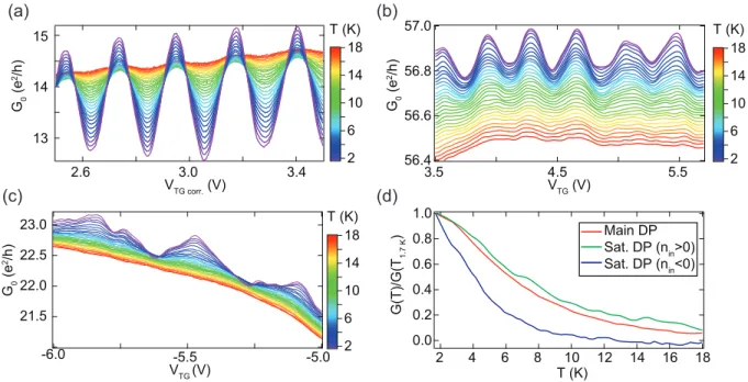
Temperature dependence of Fabry-P´ erot resonances
(a) (b)
(c)
15
14
13
3.4 3.0
2.6 3.5 4.5 5.5
G0 (e2/h)
57.0
56.8
56.6
56.4 G0 (e2/h)
VTG corr. (V) VTG (V)
-6.0 -5.0 23.0 22.5 22.0 21.5 G0 (e2/h)
VTG (V)
18 14 10 6 2 T (K)
-5.5
1.0 0.8 0.6 0.4 0.2
0.02 4 6 8 10 12 14 16 18
T (K) G(T)/G(T1.7 K)
18 14 10 6 2 T (K)
18 14 10 6 2 T (K)
(d)
Main DP Sat. DP (nin>0) Sat. DP (nin<0)
FIG. S5. Temperature dependence of the FP resonances FP resonances across the a, main DP and the two satellite DPs where b, n
in< 0 and c, n
in> 0 as a function of temperature. d, Oscillation amplitude as a function of temperature renormalized by the value measured at base temperature (T ∼ 1.7 K). While the FP resonances remains very fainth even at T ∼ 20 K for (a) and (b), it disappears already around T ∼ 10 K in the case of (c).
The temperature dependence of the various FP resonances are shown in Fig. S5. Across the main DP and the
satellite DP on the electron side (Fig. S5a,b), the temperature where the resonances disappear are in the order of
T ∼ 20 K (E ∼ 2 meV), which is on the same order of the level spacing obtained from bias spectroscopy. The
FP resonances across the satellite DP on the hole side seem to vanish at slightly lower temperatures (T ∼ 10 K,
E ∼ 1 meV).
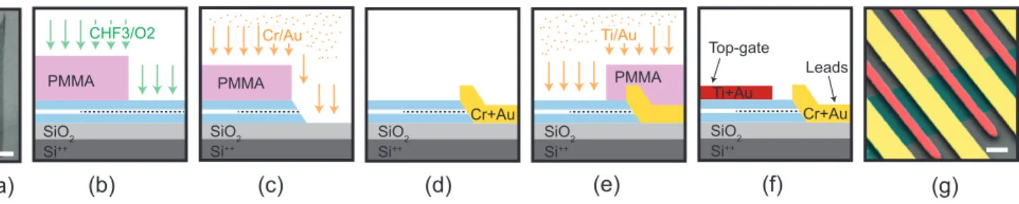
Fabrication
(a) (b) (c)
SiO2 Si++
PMMA CHF3/O2
SiO2 Si++
PMMA Cr/Au
SiO2 Si++
Cr+Au
(d)
SiO2 Si++
PMMA Ti/Au
(e)
SiO2 Si++
Cr+Au Ti+Au
Top-gate
Leads
(f) (g)
FIG. S6. Fabrication of a 2-terminal pnp-junction array. a, Exfoliated graphene flake having a width of ∼ 1.5 µm. Scale- bar equals 5 µm. b-d, The assembly of the hBN-graphene-hBN heterostructure and subsequent etching of the side-contacts follows mostly the procedure described in [15]. e,f, Establishing the local top-gates without the need to etch the encapsulated graphene. g, False-color SEM image with side-contacts (yellow), top-gates (red) and the graphene encapsulated between two layers of hBN (cyan). Scale-bar equals 500 nm.
The fabrication of the hBN-graphene-hBN heterostructure follows Ref. [15] in most steps with some variations and extensions as explained in the following. Exfoliation is done on a Si
++/SiO
2substrate with a 315 nm-thick oxide, using the scotch-tape technique. The chips were previously cleaned using Piranha solution (98% H
2SO
4and 30%
H
2O
2in a ratio of 3:1). For the assembly of the heterostructure, we choose only graphene-flakes having a width not exceeding 2 µm as shown in Fig. S6a. This is beneficial when fabricating the local top-gates. Next, self-aligned side-contacts are established to the graphene as shown in Fig. S6b-d. Self-aligned means that the same PMMA mask is used for etching the hBN-graphene-hBN heterostructure and subsequent evaporation of the Cr/Au (10 nm/50 nm) contacts. This leads to very transparent contacts (∼ 50 − 100 Ω · µm) since the exposed graphene edge never comes into contact with any solvent or polymer. It is worth mentioning that we use cold-development (T ∼ 3 − 5
◦C) with IPA:H
2O (7:3) to reduce cracking of the PMMA on hBN [16, 17]. In the last step, the local top-gates are evaporated (Fig. S6e). Since a narrow graphene flake was chosen in the very beginning of the fabrication, no etching step to shape the graphene is needed. The spacing between the top-gate and graphene is defined only by the top-hBN layer which can be chosen very thin. Therefore we can achieve high carrier concentrations and we are able to establish relativly sharp pn-junctions.
In order to fabricate the Moir´ e superlattice, straight edges of the graphene and the top-hBN are aligned with respect to each other [18]. With this technique, a rotation angle between top-hBN and graphene of less than 1 degree can be achieved with a corresponding superlattice period of ∼ 10 nm [19]. The aligned graphene-hBN stack is then placed down a large angular misalignment.
Theoretical Model
The transport simulation used in this study is identical to the one used in Ref. [4]. More information on the calculations are summarized in the supplementary information of Ref. [4] or in more detail in Ref. [20, 21]. We note that in order to have constructive/destructive interference, two interfaces with a non-zero reflection coefficient are required. Since the contacts dope the graphene in their vicinity into n type, we observe stronger oscillations in the pnp and ppp compared to the npn and nnn cases. The better visibility is due to the additional pn-junction close to the contact, which leads to larger reflectivity. This can be seen both in experiment and simulation.
Sharp vs. smooth pn-junction
A symmetric pn-junction is commonly regarded as sharp or smooth by the definition of λ
Fd or λ
Fd, respectively, where d is the transition region from n - to p-doping and λ
F= 2 p
π/n is the Fermi wavelength far from
the pn-junction, where the carrier density is homogeneous.
-4 0 4 d/dVBG G (e2/h)
-30 0
VBG (V) 15 30 -15
-20 0 20
d/dVBG G (e2/h)
-30 0
VBG (V) 15 30 -15
(a) (b)
pp’p
nn’n pnp
npn
pp’p
nn’n pnp
npn
x (nm)
−400 −200 0 200 400
−2
−1 0 1 2 3 4x10¹⁶
n(x) (m-2)
(c)
(Vtg,Vbg)=(1,-30)V (4,15)V
“sharper”
“smoother”
4 2 0 -2 -4 VTG (V)
4 2 0 -2 -4 VTG (V)
FIG. S7. Theoretical transport simulation. a, The numerical derivative of the conductance as a function of global back- gate and local top-gate of the experimental data. b, Comparable map as in (a) obtained from transport simulation which reproduces the experimental data very well. c, Calculated density-profiles throughout the sample for different gate-voltages as indicated in (b) with red.
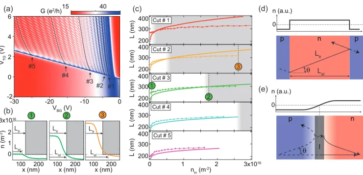
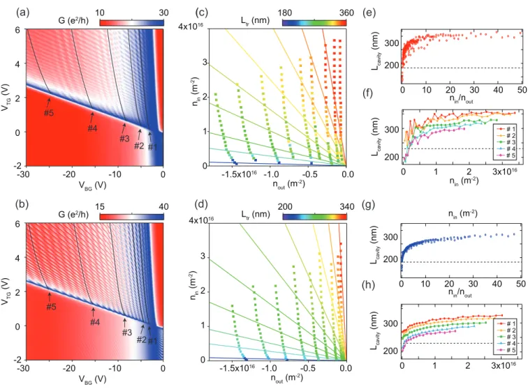
Definition of the cavity length
40 G (e2/h)15
6 4 2 0
-2-30 -20 -10 0
VBG (V) VTG (V)
#2 #1
#4 #3
#5
200
L (nm)
300 400
nin (m-2) 3x10¹⁶ 1
0 2
200
L (nm)
300 400200
L (nm)
300 400200
L (nm)
300 400200 300 400
L (nm)
Ltr Lel
0 n (a.u.)
n p
θ l
0 n (a.u.)
n
p p
L
elL
trθ
n (m-2) 3x10¹⁶
0 1 2
x (nm) 100 200
Ltr Ltr Lel Lel
1 2 3
(a) (c)
(b)
(d)
(e)
3
2 1
Cut # 1
Cut # 2
Cut # 4
Cut # 5 Cut # 3
x (nm) 100 200
x (nm) 100 200
FIG. S8. Definition of the cavity length. a, Transport simulation reproducing the Fabry-Perot pattern observed for the regular pnp-junction in the experiment. The linecuts indicated with 1-5 are at identical positions with those extracted from the experiment. b, Three different density profiles where L
tr> L
el, L
tr= L
eland L
tr< L
el. The inner cavity is centred around x = 0 nm. c, Comparison of the extracted cavity length from the transport simulation (L
tr) using Equation (4) (line + markers) and the cavity length extracted from electrostatic calculations (L
el, bold line) for different cuts as indicated in (a). Depending on the inner inner and outer cavity-doping, L
trcan be larger or smaller than L
el. The two models are in best agreement for high doping of n
inand n
outsuch as shown for cut 5. d,e, Further small corrections which are responsible that the extracted cavity length L
trdeviates from L
el.
In the main text, the cavity length was extracted from consecutive peaks of constructive interference in the mea-
surement. However, the extracted cavity length in this case does not correspond to the distance between the two
points of zero charge-carrier density of the left and right pn -interface, as one might think. Here we elaborate on the
difference between the cavity length extracted from transport measurements and from electrostatic considerations.
Furthermore, two additional aspects which account for minor corrections on the cavity length are discussed.
Cavity length from electrostatic calculations (L
el)
Probably the most straight-forward definition of the cavity length in a pnp-junction is by the distance between the two points where the charge-carrier density is zero. In the simulation, for every set of (V
BG,V
TG) a density profile along the x-axis (defined perpendicular to the pn-junction, x = 0 is centred in the middle of the top-gate) was calculated based on the quantum capacitance model for graphene[21] with classical self-partial capacitances simulated using FEniCS[22] and Gmsh[23].
Three exemplary profiles (zoom near the right pn-junction of the inner cavity) are shown in Fig. S8b and further examples can be seen in Fig.S7c. Finally the evolution of L
el(inner cavity) as a function of n
infor the linecuts indicated in Fig. S8a is shown in Fig. S8c (bold lines). The transport simulation in Fig. S8a is based on the same electrostatic model.
Cavity length from transport measurements (L
tr)
3 2 1
0
nout (m-2) nin (m-2)
-1.5x10¹⁶ -1.0 -0.5 0.0 Ltr (nm)
(a)
4x10¹⁶
Lcavity 200
(nm) 300
nin (m-2) 3x10¹⁶ 1
0 2
# 1 # 2 # 3 # 4 # 5 # 1 # 2 # 3 # 4 # 5
nin/nout 10
0 20
200 300 Lcavity (nm)
30 40 50
30 G (e2/h) 10
6 4 2 0
-2-30 -20 -10 0
VBG (V) VTG (V)
40 G (e2/h) 15
6 4 2 0
-2-30 -20 -10 0
VBG (V) VTG (V)
#2#1
#4 #3
#5
#2#1
#4 #3
#5
360 180
Ltr (nm) 200 340
3 2 1
0
nout (m-2) nin (m-2)
-1.5x10¹⁶ -1.0 -0.5 0.0 4x10¹⁶
Lcavity200
(nm) 300
nin (m-2)
3x10¹⁶ 1
0 2
nin/nout 10
0 20
200 300 Lcavity (nm)
30 40 50
(c)
( (e)
(f)
(b) (d) (g)
(h)
FIG. S9. Cavity length as a function of (n
in,n
out) or n
in/n
outfor experiment (top row) and theory (bottom
row). a,b, Conduction map as a function of V
BGand V
TG. Selected linecuts are indicated. c,d, L
tras a function of n
inand
n
out. The solid lines are a guide to the eye for a constant cavity length. e,g, The same data as in (c,d) plotted as the ratio
n
in/n
out. f,h, Selected linecuts as indicated in (a,b) at fixed n
out.
The cavity length extracted from the position of two neighbouring FP peaks, assuming a FP resonator with a hard-wall potential, is given by
L
tr=
√ π
√ n
j+1− √
n
j(4)
as derived in the main text. Using a box-shaped potential is an oversimplification and can lead to a difference compared to L
el. In Fig. S8b the calculated L
tris sketched in direct comparison with the calculated density-profile from electrostatics. In Fig. S8c L
tr(line + symbols) is plotted together with L
el(bold lines) where the shaded region account for L
el> L
tr.
The cavity length L
tris fixed for a given ratio of n
in/n
outas explained in the main text. The same is true for L
el, because if n
inand n
outare varied by a common factor, only the slope of the pn-junction changes, whereas the position of zero density remains constant. In Fig. S9 L
tris plotted (for experiment and theory) in various ways to see the different trends more clearly. In Fig. S9a/b the conduction map as a function of the global back-gate and local top-gate is given with selected linecuts indicated with #1 − #5. L
trextracted from various linecuts is plotted in Fig. S9c/d as a function of n
inand n
out, the positions of the corresponding FP resonances. The solid lines are a guide to the eye where L
tris constant. It can be easily seen that the condition L
tr(n
in/n
out) = const. is well fulfilled since the colors of the points showing L
trremain constant along the solid lines. The same information is replotted in Fig. S9e/g, where all points of Fig. S9c/d are plotted as a function of the ratio n
in/n
out. All values L
trfollow the same curve, independent of the position (n
in, n
out). In Fig. S9f/h selected linecuts (n
out= const., as indicated in Fig. S9a/b) are plotted against n
in. From these curves the trends of L
trfor fixed (i) n
outor (ii) n
inwas deduced as described in the main text.
Second order corrections
Besides the major difference of assuming a box-shaped hard-wall potential, there are further smaller corrections leading to a difference between L
trand L
el:
• Assume there is a density-profile as indicated in Fig. S8d. Since the trajectories contributing most to the FP signal have a finite incident angle θ (for θ = 0 one ends up with Klein-tunneling, thus no contribution to the FP [24–27]), the extracted L
tractually corresponds to the diagonal distance. Therefore the real cavity length (which is given in this case by L
el) is given by L
el= L
trcos(θ). In this case L
trover-estimates the real cavity size. Since the charge-carriers with a small incident angle (with respect to the pn-junction normal) account for most of the FP signal, this results only in a minor correction.
• As already mentioned before, the density profile is smooth and not abrupt. This leads to a bending of the charge-carrier near the n = 0 density line as sketched in Fig. S8e. Charge carrier are therefore reflected before they hit the n = 0 density line, which will make the effective cavity size shorter. The distance l can be calculated according to l = vp
y/E
x[28]. However, since the trajectories of the charge carriers are bent, and in addition the density is varying while approaching the pn -junction, it is hard to make any statements if this effect will lead to an over- or under-estimation of the cavity size.
Conclusion
Using Equation (4) to extract the cavity length from FP resonances, gives slightly different results than using the
definition based on simulated carrier densities. The extracted cavity lengths L
trand L
elare only in good agreement
(over a longer density range) when the outer and inner cavities are highly doped. In our experiment this condition
is best satisfied for Cut 5 as shown in Fig. S8c. This can be understood since at high doping the transition from p-
to n- region is sharper than for low doping, thus best resembling a box-potential. Nevertheless, using Equation (4)
for the whole gate/density range is justified by the fact that for both, experiment and theory, the same quantity is
extracted.
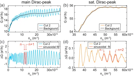
18 16 14 12 10
2 1 0 -1
nin (m-2) 30x1015 10
0 20
G (e2/h)∆G (e2/h)
Cut 2 Backgound
n n+1
main Dirac-peak sat. Dirac-peak
Cut 2 sinusoidal fit
56 55
54 Backgound
Cut 2
sinusoidal fit Cut 2 0.1
0.0
-0.1
nin (m-2) 60x1015 45
35 40 50 55
∆G (e2/h)G (e2/h)
n n+2
(a) (b)
(c)
nin (m-2)(d)
30x1015 10
0 20
nin (m-2) 60x1015 45
35 40 50 55
FIG. S10. Algorithm to extract the exact peak-position of the Fabry-Perot resonances of a pnp-junction. a, FP resonances (Cut 2, Fig. S9a) across the main DP (cyan) and the corresponding background (black) obtained by smoothening.
b, FP resonances across the satellite DP (orange) where the inner cavity is tuned above the satellite DP with the corresponding background (black). c,d, Net oscillations (∆G) with sinusoidal fit to extract the exact peak-positions.
Extracting the peak-position from Fabry-Perot resonances
In order to extract the exact position of the FP resonances, the background of the line-profiles was subtracted by smoothening the linecut sufficiently (black line in Fig. S10a,b). The net resonances (∆G) were fitted with a sinusoidal curve depicted in Fig. S10c,d respectively. Since the FP oscillation of the satellite DP is much weaker and reveals a higher signal-to-noise ratio (compared to the FP measured across the main DP) the fitting-range was enlarged.
Fabry-P´ erot in inner and outer cavity across the satellite Dirac Peak
-2 3 8x10¹⁶
d/dnout G (e2/h) d/dnin G (e2/h)-2 3x10¹⁶
5 4 2 7x10¹⁶
nout (m-2) nin (m-2)
36.6 43.7 G (e2/h)
25x1015 15 20
10 6
3
(a) (b) (c)
5 4 2 7x10¹⁶
nout (m-2) nin (m-2)
25x1015
15 20
10 6
3
5 4 2 7x10¹⁶
nout (m-2) nin (m-2)
25x1015 15 20
10 6
3
FIG. S11. FP resonances in the inner and outer cavities across the satellite DP. a, Conduction as a function of the charge-carrier density in the inner and outer cavity. The position of the satellite DP is indicated with the dashed, purple line.
Numerical derivative along b, n
outand c, n
inreveal the conduction resonances in the outer and inner cavity respectively. Two representative line profiles of the numerical derivative are shown in orange.
Compared to the FP resonances observed across the main DP (bipolar region), the visibility for the resonances in
the outer cavities is less pronounced compared to the one in the inner cavity. Extracting the cavity-length from the
linecuts indicated in Fig. S11b and S11c confirms that the observed FP resonances belong to resonances in the outer
and inner cavity respectively.
Energy scales in the Moir´ e mini-bands and residual doping
(d) (a)
E (ħvFb)
Model 1
0.5
0.0
-0.5
E~50 meV E~190 meV
0 1 2 3
DOS (b/(ħvF�))
E~225 meV
Model 2
E~0 meV E (ħvFb)
0.5
0.0
-0.5
0 1 2 3
DOS (b/(ħvF�))
E~217 meV
Model 3
E~90 meV E (ħvFb)
0.5
0.0
-0.5
0 1 2 3
DOS (b/(ħvF�))
(b) (c)
30 25
20
15
81014 2 4 6 8 2 4 6 8 1015 1016 l∆ninl (m-2)
G (e2/h)
lninl>lnsat. DPl lninl<lnsat. DPl