Supplemental Material for
Fabry-P´erot interference in gapped bilayer graphene with broken anti-Klein tunneling
Anastasia Varlet,1,∗Ming-Hao Liu (ddd),2Viktor Krueckl,2Dominik Bischoff,1Pauline Simonet,1Kenji Watanabe,3Takashi Taniguchi,3Klaus Richter,2Klaus Ensslin,1and Thomas Ihn1
1Solid State Physics Laboratory, ETH Z¨urich, 8093 Z¨urich, Switzerland
2Institut f¨ur Theoretische Physik, Universit¨at Regensburg, D-93040 Regensburg, Germany
3Advanced Materials Laboratory, National Institute for Materials Science, 1-1 Namiki, Tsukuba 305-0044, Japan (Dated: June 13, 2014)
I. THEORY
A. Electrostatic model for the device
We apply the parallel-plate capacitor model to deduce the top- and back-gate efficiencies for our bilayer graphene (BLG) device. The thicknesses of the top and bottom hexagonal boron nitride (h-BN) layers ared(top)h-BN=30 nm andd(bot)h-BN= 23 nm, respectively, and we adoptεrh-BN=3.0 as their dielec- tric constant. The topgate capacitance for area C is then given by
CTG
e =εrh-BNε0
ed(top)h-BN =5.53×1011cm−2V−1. (S1) Together with the SiO2 substrate with thickness dSiO2 = 285 nm and dielectric constantεrSiO2 =3.9, the backgate ca- pacitance is given by
CBG e =ε0
e
dh-BN(bot) εrh-BN+
dSiO2 εrSiO2
!−1
=6.53×1010cm−2V−1. (S2) Next, we deduce the intrinsic doping by inspecting the full conductance map. We assume that in regionX(X=L,C,R), the residual carrier density is uniformly described byn0X. In Fig. 1(d) of the main text, the conductance dip at VTG=
−2.1 V along theVBG=0 V horizontal line cut suggests n0C=CTG
e ×2.1 V=1.16×1012cm−2. (S3) For the outer areas L and R, the residual density is deduced from the two topgate-independent horizontal Dirac lines, one atVBG=−7.6 V, suggesting
n0L=CBG
e ×7.6 V=4.97×1011cm−2, (S4) and one atVBG=−14 V, suggesting
n0R=CBG
e ×14 V=9.15×1011cm−2. (S5)
∗varleta@phys.ethz.ch
Collecting Eqs. (S1)–(S5), we obtain the gate-dependent car- rier density:
nX(VTG,VBG) =
CTG
e VTG+CBG
e VBG+n0X, X=C CBG
e VBG+n0X, X=L,R .
(S6)
B. Asymmetry parameter
To calculate the gate-dependent asymmetry parameter for our device, we follow the review by McCann and Koshino [1]. Let us temporarily suppress the area indexX and con- sider the total carrier densityn=nt+nb+n0, wherentis the topgate contribution,nbis the backgate contribution, and the intrinsic doping is assumed to be equally distributed in the two graphene layers:nb0=nt0=n0/2. This assumption allows us to rewrite Eq. (65) of Ref.1as
Uext= γ1
n⊥Λ(nb−nt), (S7) where
Λ= c0e2n⊥ 2γ1εrε0
(S8) is the screening parameter, and
n⊥= γ12
πh¯2v2F (S9) is the characteristic carrier density. In Eqs. (S7)–(S9), γ1= 0.39 eV is the nearest-neighbor hopping for the interlayer cou- pling, c0≈0.335 nm is the interlayer spacing of the BLG, εr =1 is the effective dielectric constant between the two layers of BLG, andvF is the Fermi velocity of graphene re- lated to the tight-binding parameters through ¯hvF= (3/2)ta, t ≈3 eV being the nearest-neighbor intralayer hopping and a≈0.142 nm being the carbon-carbon bond length. Using Eq. (S7), Eq. (74) of Ref.1reads
n⊥u Λ(nb−nt)≈
1−Λ 2ln
|n| 2n⊥+1
2 s
n n⊥
2
+u 2
2
−1
, (S10)
2 whereu=U/γ1is defined. Finally, we rewrite Eq. (S10) as
u=Λ(nb−nt) n⊥
1−Λ 2ln
|n| 2n⊥+1
2 s
n n⊥
2
+u 2
2
−1
(S11) in order to avoid the divergence atnb=nt.
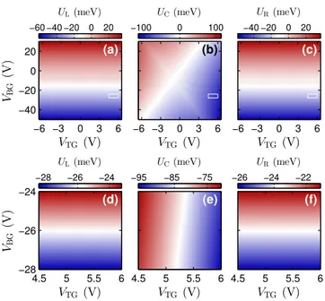
The nonlinear Eq. (S11) can be solved numerically to ob- tain the asymmetry parameterU =γ1u, when the inputsnt, nb, and n0 are given. Using Eqs. (S3)–(S6) we obtain the asymmetry parametersUXfor the respective areasX=L,C,R of our BLG device. Numerical results are shown in Fig.S1.
The actual size of the band gapUgis related withUthrough Ug=|U|γ1/q
γ12+U2.
C. Local energy band offset
From the calculated carrier densitynX and asymmetry pa- rameterUX based on the electrostatic model, the band offset VXfor areaXis given by
VTG (V)
VBG(V) (a)
−6 −3 0 3 6
−40
−20 0 20
UL(meV)
−60 −40 −20 0 20
VTG (V) (b)
−6 −3 0 3 6
UC(meV)
−100 0 100
VTG(V) (c)
−6 −3 0 3 6
UR(meV)
−40 −20 0 20
VTG (V)
VBG(V) (d)
4.5 5 5.5 6
−28
−26
−24
UL(meV)
−28 −26 −24
VTG (V) (e)
4.5 5 5.5 6
UC(meV)
−95 −85 −75
VTG(V) (f)
4.5 5 5.5 6
UR(meV)
−26 −24 −22
FIG. S1. Asymmetry parameterUX in regionX=L,C,R of the de- vice as a function top- and back-gate voltages. Panels (a)–(c) in the upper row show the full range, where the white boxes mark zoom-in range for panels (d)–(f) in the lower row.
VX=−sgn(nX) v u u tγ12
2 +UX2
4 +h¯2v2Fπ|nX| −γ1
2 s
γ12+ (2¯hvF)2π|nX|
1+UX2 γ12
, (S12)
which is obtained by replacing the two-dimensional wave vec- tork by p
π|nX| in the energy dispersionE(k) for gapped BLG [1] and by adding the minus sign. Application of Eq.
(S12) on the diagonal matrix elements of the model Hamilto- nian for transport calculation therefore fixes the global Fermi level at energyE=0, at which the transmission function is evaluated (linear-response transport).
D. Berry phase in gapped bilayer graphene
In order to take into account the characteristic band struc- ture of the BLG, we incorporate the Berry phase into the reso- nance condition of the Fabry-P´erot (FP) oscillations in Eq. (1) of the main text. Therefore, we describe the low energy exci- tations of BLG for a single valley by the Hamiltonian [1],
H=
U/2 hv¯ Fk− 0 0
¯
hvFk+ U/2 γ1 0 0 γ1 −U/2 ¯hvFk− 0 0 hv¯ Fk+ −U/2
, (S13)
using the layer coupling γ1, the asymmetry U and k± = kx±iky. Without losing generality we focus on a single val- ley, as the results of the second one can be obtained by time
reversal, leading to an inverted Berry phase. The four eigen- statesψσ(k)ofH can be associated with the different bands, which we label asσ=n2,n1,p1,p2 from high to low energy.
[For the present discussion, the relevant bands are the two in- ner bandsn1,p1 as those sketched in Fig. 1(f) of the main text.] Using these eigenstates, we can calculate the Berry cur- vature [2],
Aσ(k) =−ihψσ(k)|∇kψσ(k)i, (S14) and the corresponding Berry phase
Φσ= I
k=const
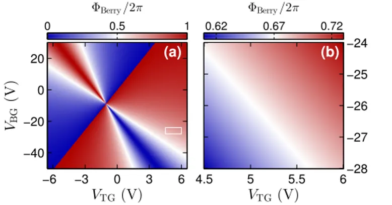
Aσ(k)·dk, (S15) which describes the additional phase the stateψσ(k)picks up upon traveling adiabatically one complete circle in momen- tum space. Since transport within the central area C in the pn’p regime is carried only by then1 band as sketched in Fig. 1(f) of the main text, FP oscillations pick up the Berry phaseΦBerry=Φσ=n1. This additional phase changes upon varying the top- and back-gate voltages in the whole possible range from 0 to 2π, as shown in Fig.S2(a). Also for the ex- perimental transport data presented in Fig. 2(a) of the main text, the Berry phaseΦBerry is not constant but takes values
3
VTG(V) VBG(V)
(a)
−6 −3 0 3 6
−40
−20 0 20
ΦBerry/2π
0 0.5 1
VTG(V) (b)
4.5 5 5.5 6
−28
−27
−26
−25
−24 ΦBerry/2π
0.62 0.67 0.72
FIG. S2. (a) Berry phase as a function of top- and back-gate voltages for the state closest to the avoided crossing at the Dirac point within the dual-gated area C of the device. (b) Zoom-in of the bipolar block indicated by the white box in (a).
between 1.22π and 1.46π, as presented in Fig.S2(b). Conse- quently, the Berry phase has to be included in the resonance condition in order to achieve a precise prediction of the con- ductance maxima.
II. EXPERIMENT
A. Oscillations: conductance VS transconductance signals In the manuscript, we characterized the FP oscillations by studying the measured transconductance signal. The reason is a better visibility in the signal. However, the oscillations are already visible in conductance, as shown in Fig. S3(a-c).
Their visibility is only weakened by the ascending slope (see Fig. S3(c)). The same analysis as the one done in the main manuscript could be performed with the conductance data.
B. Density dependence
As explained in [3], Fabry-P´erot interference should give rise to oscillations spaced in density by ∆n=2√πnC/LC, wherenC is the density in dual-gated area andLC the width of the cavity. In this case,LC=1.1µm. To confirm the origin of the oscillatory signal, we therefore study the peak spac- ing dependence, as done in the main text with Fig. 2(c), but on a broader range of voltages. To highlight the square root dependence, we show in Fig. S4(a) more data points: each color corresponds to a different backgate voltage value. We see that the observed behavior follows the expected behavior, represented with the black dashed line, reasonably well.
C. Temperature dependence of the Fabry-P´erot oscillations We observed in Fig. 4(c) of the main text that, at high tem- peratures, the oscillation amplitude saturates. This means that
4.5 5 5.5 6
9.2 9.6
VTG(V)
G(e²/h)
10 8,8 G(e²/h)
(a) (b)
(c) (d)
4.5 5 5.5 6
VBG(V)
4.5 5 5.5 6
-28 -27 -25 -24
15 -15 dG/dVTG(e²/h.V)
4.5 5 5.5 6
-15 -5 5 15
VTG(V) dG/dVTG(e²/h.V)
VBG=-26V VBG=-26V VTG(V) VTG(V)
FIG. S3. (color online). (a) Conductance map corresponding to the measurement shown in Fig. 2(a) of the main text: the oscillations are already visible. (b) Normalized transconductance map (same as Fig.
2(a) of the main text, for comparison): the oscillations appear more clearly. (c)/(d) Cut taken from (a)/(b) atVBG=−26 V.
part of the oscillations have a non-coherent origin and for fur- ther analysis, we subtract the highest temperature curve from each temperature signal.
To get a better insight in the observed temperature depen- dence, we consider the derivative of the Fermi-Dirac distribu- tion:
∂f
∂EF = 1 4kBT
1 cosh2
E−EF
2kBT
, (S16)
whereT is the fixed temperature (estimated from the recorded Allen-Bradley resistance value) andE=h¯2πnC/2m∗.
Convoluting each measured trace with the derivative of the Fermi-Dirac distribution atT =Tmeasured, we notice that we do not recover the full amplitude of the measured signal. This can be due to a wrong evaluation of the energy (maybe due to screening or deformation of the band structure by trigonal warping, which are not taken into account here). To correct this parameter, we fit the convoluted curve using the tempera- ture as a free parameter. The result is shown in Fig.S5(a).
Using these corrected temperatures, we now compare the standard deviation of each curve with the thermal damping term:
dG
dVTG∼A2π2kbT
∆E
1 sinh
2π2kbT
∆E
, (S17)
4 (a)
3.8 4 4.2 4.4 4.6 4.8 5 5.2
3 3.5 4 4.5 5 5.5 6
(x 1010cm-2)
∆n(x1010cm-2)
2
VBG= -20V VBG= -25,9 V VBG= -28 V VBG= -29 V VBG= -30,6 V
π nc Lc
FIG. S4. (color online). (a) Dependence of the peak spacing as a function of density for different backgate voltages (different colors).
The expected behavior is displayed in black dashed line.
(a)
(b)
0 1 2 3 4 5 6 7
0
Tmeasured Tfit
0 20 40 60 80
0 0.2 0.4 0.6 0.8 1
∆E/kBT
Thermaldamping
Data
Thermal damping term
2 4 6
FIG. S5. (color online). (a) Result of the temperature fit compared to the measured temperature. (b) Using the fitted temperature value, we compare the behavior of our signal with the thermal damping (black dashed line).
withAa scaling parameter and∆E is the averaged period of the oscillations on the studied interval. The result is displayed in Fig.S5(b), withA=0.2 and∆E=1.2 meV. We find good agreement between the data points and the model and there- fore attribute the damping of the oscillations as a function of temperature to thermal averaging.
[1] E. McCann and M. Koshino,Rep. on Progr. in Phys.76, 056503 (2013).
[2]M. V. Berry,Proc. R. Soc. Lond. A392, 45 (1984).
[3]A. L. Grushina, D.-K. Ki, and A. F. Morpurgo,Appl. Phys. Lett.
102, 223102 (2013).