Fabry-Pérot Interference in Gapped Bilayer Graphene with Broken Anti-Klein Tunneling
Anastasia Varlet,1,* Ming-Hao Liu (劉明豪),2 Viktor Krueckl,2 Dominik Bischoff,1 Pauline Simonet,1 Kenji Watanabe,3 Takashi Taniguchi,3 Klaus Richter,2Klaus Ensslin,1 and Thomas Ihn1
1Solid State Physics Laboratory, ETH Zürich, 8093 Zürich, Switzerland
2Institut für Theoretische Physik, Universität Regensburg, D-93040 Regensburg, Germany
3Advanced Materials Laboratory, National Institute for Materials Science, 1-1 Namiki, Tsukuba 305-0044, Japan (Received 13 June 2014; published 8 September 2014)
We report the experimental observation of Fabry-Pérot interference in the conductance of a gate-defined cavity in a dual-gated bilayer graphene device. The high quality of the bilayer graphene flake, combined with the device’s electrical robustness provided by the encapsulation between two hexagonal boron nitride layers, allows us to observe ballistic phase-coherent transport through a1-μm-long cavity. We confirm the origin of the observed interference pattern by comparing to tight-binding calculations accounting for the gate-tunable band gap. The good agreement between experiment and theory, free of tuning parameters, further verifies that a gap opens in our device. The gap is shown to destroy the perfect reflection for electrons traversing the barrier with normal incidence (anti-Klein tunneling). The broken anti-Klein tunneling implies that the Berry phase, which is found to vary with the gate voltages, is always involved in the Fabry-Pérot oscillations regardless of the magnetic field, in sharp contrast with single-layer graphene.
DOI:10.1103/PhysRevLett.113.116601 PACS numbers: 72.80.Vp, 73.23.-b
Interference of particles is a manifestation of the wave nature of matter. A well-known realization is the double-slit experiment, which cannot be described by the laws of Newtonian mechanics, but requires a full quantum descrip- tion. This experiment has been performed with photons [1,2], electrons[3], and even molecules[4]. Another setting widely used in optics is the Fabry-Pérot (FP) interferom- eter, where a photon bounces back and forth between two coplanar semitransparent mirrors. Partial waves transmitted after a distinct number of reflections within this cavity interfere and give rise to an oscillatory intensity of the transmitted beam as the mirror separation or the particle energy is varied.
In solid-state physics, graphene has proven to be a sui- table material for probing electron interference at cryogenic temperatures [5,6]. However, in single-layer graphene (SLG) the realization of FP interferometers is challenging.
The absence of a band gap and the Klein tunneling hamper the efficiency of sharp potential steps between then- and p-type regions, which play the role of the interferometer mirrors[7–9]. Theory suggests that smooth barriers enhance the visibility of interference[10,11]due to Klein collimation [12]. Recently, ultraclean suspended SLG devices have shown FP interference with stunning contrast using cavity sizes of more than1μm[13–15].
In bilayer graphene (BLG) potential steps between n- and p-type regions lead to evanescent interface states resulting in a zero-transmission at normal incidence, known as anti-Klein tunneling [7]. Furthermore, in BLG a band gap can be induced by a transverse electric field[16–19].
The Berry phase ofπ in SLG has been predicted[20]and observed[10]to cause a phase jump ofπin the FP fringes
at weak magnetic field (B). In gapless BLG the Berry phase is known to be2π, but it is yet to be understood how the Berry phase in gapped BLG influences the FP interference.
In this Letter, we investigate the FP interference in gapped BLG. Comparing experiment and theory, we reveal the roles played by the anti-Klein tunneling, the gap, and the Berry phase. We perform transport measurements on a locally dual-gated BLG encapsulated between hexagonal boron nitride (h-BN) flakes. The high quality of the dual- gated area allows us to observe FP interference in the bipolar regime. The origin of the measured oscillations is confirmed by ballistic transport simulations. The depend- encies of the interference patterns on the carrier density, the B field, the applied bias, and the temperature are inves- tigated. We consistently find signatures of ballistic phase- coherent transport over a1μm distance and highlight the very different tunneling behavior of BLG and SLG.
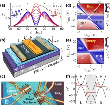
We first point out a simple but striking theoretical fact regarding a single junction. The perfect reflection across a bipolar potential step in BLG was predicted in Ref.[7], in the absence of the gap. Little attention has been paid, however, to the fact that the presence of the gap destroys the perfect reflection at normal incidence[21,22]. By calculat- ing the angle-resolved transmissionTðϕÞ(Green’s function method based on a tight-binding model as in Ref.[23]), we find that a nonzero normal incidence transmission can be recovered by introducing a gap. As illustrated in Fig.1(a), Tðϕ¼0Þ increases with the so-called asymmetry param- eter U defined as the on-site energy difference between the two graphene layers[24]. Here we consider transport through an ideal, symmetric, sharpn-p junction with the potential step height fixed at 0.2 eV andUincreasing from
zero to 0.1 eV. Because of the twofold valley degeneracy incorporated in the tight-binding model, the transmission functionT has a maximum possible value of 2 within the single-band regime (i.e., energy jEj≤γ1, γ1≈0.39eV being the nearest-neighbor interlayer hopping). As seen in Fig. 1(a), Tð0Þ ¼0 only when U¼0, which is the celebrated anti-Klein tunneling. It acquires finite values whenU≠0. Recovering a finiteTð0Þwith increasing band gap thus reveals the counterintuitive role played by U, which increases the transmission by suppressing anti-Klein tunneling.
The investigated device, sketched in Figs.1(b)and1(c) (right device), consists of a h-BN/BLG/h-BN stack deposited on a Si=SiO2substrate, prepared as presented in Ref.[25], using the transfer technique described in Ref. [26]. The measurements were performed at a temperature of 1.6 K in a two-terminal configuration (inner Ohmic contacts). Unless stated otherwise, a constant bias voltage was applied sym- metrically between the Ohmic contacts [SandDin Fig.1(b)]
and the current was measured. Modulating the top-gate voltage with an ac component enabled the measurement of the normalized transconductancedG=dVTG.
Our device consists of three areas: two outer areas (denoted as L and R, of length lL¼lR¼0.95μm) simultaneously tuned by the voltageVBG, and the central
area (denoted asC, lC¼1.1 μm) which is tuned by both top and back gate (VTG, VBG). The two-dimensional map presented in Fig.1(d)shows the conductance of the device measured as a function of bothVTGandVBG. Depending on the applied voltages, four different polarity combinations are possible: two with same polarities (pp0pandnn0n—the prime referring to region C) and two with opposite ones (np0nandpn0p). The charge neutrality point of the dual- gated area evolves along the so-called displacement fieldD~ axis. While increasingjD~j, the conductance at the charge neutrality point decreases because a gap is opened. This band gap has been characterized with temperature- dependent measurements, which provided the activated gap size ofEgap¼2meV at VBG ¼28V (corresponding toD~ ¼1.1V=nm). As previously reported[27–30], trans- port in the gap is dominated by hopping, preventing the experimental determination of the real gap size.
Our calculations for the gate-dependent conductance use a Green’s function formalism[13,31]based on the nearest- neighbor tight-binding model for BLG [32,33] with the on-site energy profile extracted from the gate-modulated carrier density. To relate the carrier density to the gate voltages in the respective areas, we adopt a parallel-plate capacitance model[34]. In areaX(X ¼L; C; R), the carrier densitynX¼nXðVTG; VBGÞis composed of top-gate con- tribution ntX (only for X¼C), back-gate contribution nbX, and intrinsic doping contribution n0X. Following the tight-binding theory of the gap[24], the inputs ofntX, nbX, n0X allow us to compute the asymmetry parameters UXðVTG; VBGÞ[34]. Finally, withnXandUX, the band offset for regionX to be added to the diagonal matrix elements (on-site energy) of the tight-binding Hamiltonian VX is calculated (see[34]for the expression ofVX): this fixes the global Fermi level at energyE¼0where linear-response transport occurs.
As an example illustrating the model, the band diagram at gate voltages ðVTG; VBGÞ ¼ ð5;−35Þ V is sketched in Fig.1(f), where the band offset levelVXtakes as inputsnX and UX. To keep the model as simple as possible, we neglect stray fields of the top gate and assume the potential profile to be ideally flat and sharp. We focus on the trans- port property of the dual-gated region, modelingLandR as semi-infinite leads and regarding C as the scattering region [with the only exception in Fig. 3(e); see below].
Such a simplified model taking into account the ideal band gap[24]turns out to work surprisingly well, as the main features of the measured conductance map [Fig.1(d)] are well captured by our calculation shown in Fig.1(e). Note that different from Ref.[13], throughout this work we will not worry about mode counting, and will concentrate only on the normalized conductanceg(with maximum of 2 due to valley degeneracy).
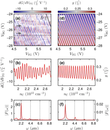
We now focus on thepn0pregime: Fig.2(a)depicts the normalized transconductance, showing a pronounced oscil- latory behavior (already visible in the conductance[34]).
FIG. 1 (color online). (a) Transmission T as a function of the incidence angle ϕ for an electron traversing a symmetric, sharp np junction, with changing asymmetry parameters U¼0;0.01;…;0.1eV. (b) Schematics of the device: a BLG flake is sandwiched between two h-BN layers. (c) Optical microscope image of two devices fabricated from the same flakes. The measurements were carried out on the right device.
(d) Conductance map measured at 1.6 K. (e) Normalized conductance map calculated based on the model depicted in (f) with the configuration marked by the star in (e).
These oscillations evolve parallel to the D~ axis [for comparison, the slope of the D~ axis is displayed in Fig. 2(a)as a black line], indicating that they are related to the dual-gated part. In Fig. 2(b), an example of a transconductance trace taken atVBG¼−26.7V is shown.
To confirm the origin of the oscillatory signal, we analyze the oscillation frequency of Fig.2(b)by first projecting the transconductance from the displayed density axis,nC, onto the wave-vector axis,k¼ ffiffiffiffiffiffiffiffiffiffiffi
πjnCj
p , and then performing the discrete Fourier transform from k to frequency ω space.
Since the main contribution to the FP interference is given by phase differenceΔΦ¼k2lC, the oscillation frequency is expected to be2lC¼2.2μm, which is in agreement with our observations in Fig. 2(c). Similar behavior has been observed for different density ranges in thepn0p regime, indicating the robustness of the phenomenon [34].
Figures2(d)–2(f) are the theory counterparts of exper- imental Figs.2(a)–2(c), except that the theoretical analysis is done from the normalized conductance (the calculation is ideally ballistic and therefore leads to a clear-enough
visibility). We emphasize that the calculation was done based on the simplified model illustrated in Fig.1(f), free of any tuning parameters. In Fig.2(f), additionally to the main peak, higher harmonics are visible at integer multiples of the fundamental period. The agreement between our theory and experiment is satisfactory, confirming the ballistic origin of the fringes reported in Fig.2(a)as FP interference in the dual-gated areaC.
To further understand the FP interference in BLG, we performed magnetotransport measurements and calculations in the lowB-field regime, where the feature of the conduct- ance is still dominated by FP interference without entering the quantum Hall regime. Figure3shows the measured gate- field map ofdG=dVTG(a) and the calculated one ofg(b).
Despite some differences in theB-field dependence of the FP fringes in the two maps for the field range ofjBzj≲20mT, (i) the number of oscillation periods and (ii) the field dependence for the range20mT≲jBzj≲60mT, are con- sistent. The former can be directly counted (both 17 stripes), while the latter can be more clearly seen by comparing Figs.3(c)and3(d)that are zoom-in plots from Figs.3(a)and 3(b), respectively, indicated by the dashed boxes therein.
To elucidate the peculiar field behavior observed only in the experimental map of Fig. 3(a) at jBzj≲20mT, we investigate the accumulated phases for a closed loop in the dual-gated cavity C given by a classical trajectory encircling, arising from backscattering at the interfaces, the area δA, as sketched in the inset of Fig. 3(b). The total phase can be decomposed into a kinetic part ΦWKB, the FIG. 2 (color online). (a) Measured transconductance and (d)
calculated normalized conductance in thepn0pregion. In (a), the gray arrows indicate faint horizontal patterns which originate from theLandRregions and the slope of theD~ axis is shown with a black line. (b) and (e) Cut along the dashed line in (a) and (d). By projecting from the density nC onto the wave-vector k axis, the discrete Fourier transforms FðωÞ of (b) and (e) are shown in (c) and (f), respectively, both of which exhibit a sharp peak at frequency ω¼2.2μm, which is precisely twice the cavity length2lC.
FIG. 3 (color online). (a) Measured and (b) calculatedB-field dependence of the FP oscillations atVBG¼−26.2V. Inset of (b) shows a closed loop considered in Eq.(1). Black and red dashed curves (sketched only for Bz≤0 for clarity) are numerical solutions to the resonance condition (1) with and without the Berry phase, respectively. (c) and (d) Zoom-in from (a) and (b), respectively, indicated by the black dashed boxes. (e) Calculated dg=dVTG map for a model with the scattering region simulating the fullL,C,R areas.
Aharonov-Bohm phase ΦAB ¼eBzδA=ℏ, and the Berry phase ΦBerry. Based on the phase difference between a transmitted and a twice reflected electron wave, we get the FP resonance condition
ΦWKBþΦABþΦBerry¼2πj; j∈Z; ð1Þ where theB-field dependence only enters through the first two terms. As shown in more detail in[34], our compu- tation of the Berry phase of BLG shows that it is only2πfor vanishing asymmetry UC and can generally take values between 0 and 2π depending on the carrier density nC and layer asymmetryUC. For the bipolar region presented in Fig. 2(a), ΦBerry is nearly constant, ranging between 1.22πand1.46π[34]. By numerically solving Eq.(1), we find a set of resonance contours well matching the periodicity of the FP fringes and being located quite closely to the conductance maxima [see black dashed contours in Fig.3(b)]. Furthermore, neglectingΦBerryin Eq.(1)leads to the red dashed contours, which do not coincide with the positions of constructive interference. We therefore con- clude that an effect of the Berry phase exists in the transport calculation, and is always involved independent ofBz. This is in sharp contrast to the case of SLG, where the Berry phase effect requires a weakB field in order to overcome the perfect transmission of Klein tunneling [20]. The experimentally observed phase jump of π in SLG [10]
was previously reproduced by two of us[31]based on the same method.
From the above discussion, the Berry phase can be ruled out as a possible reason for the peculiar B-field behavior observed for jBzj≲20mT in the experiment in Fig.3(a).
We next suspect that the effect originates from the outer areasLandR. While the fringes reported in Fig.2(a)have been confirmed to arise from FP interference in theCarea, theLandRareas that are independent ofVTGand slightly shorter thanCmay exhibit FP interference as well. Indeed, by a closer look at Fig. 2(a), one can identify a few horizontal patterns (see gray arrows) that are independent ofVTGand may be attributed to FP interference within the outer regions L and R. Taking the cavity length of lL¼lR ¼0.95μm, we estimate the expected voltage spacing to be around 0.6 V consistent with those horizontal patterns observable in Fig.2(a). By performing a ballistic calculation taking into account the total3μm length of the L, C, R areas, we show in Fig. 3(e) a gate-field map focusing on a smallerVTGrange. The peculiar behavior at low field close to zero is indeed recovered, supporting the idea that the outer areas are the main cause. The interplay between the different field dependencies of the FP inter- ference in the L, C, R cavities is, however, beyond the scope of the present discussion.
We now focus on the experimental bias dependence of the FP-modulated signal shown in Fig. 4(a). The oscillations undergo a linear shift as a function of the
source-drain bias. On top of this, their amplitude is modulated. To highlight this modulation, we calculate, at each bias value, the standard deviation from the mean of the signal [Fig.4(b)]. A modulation is seen, with two minima at∼0.6mV. This dependence reflects the energy aver- aging effect of the bias voltage. We may understand the situation by considering the oscillating transmission as a function of energy within the bias windoweVbias: each time the window encloses an integer number of oscillation periods, a minimum is reached in the signal.
Finally, we analyze the experimental effect of temper- atureT on the FP interference in Fig.4(c)with the range 1.37K≤T≤17.5K. We can distinguish two regimes: at low T, the effect of the temperature on the oscillation amplitude is strong; however, at higherT, the effect seems to saturate with some persistent oscillations. These almost temperature-independent features are not of coherent origin and we therefore subtract their contribution from the oscillations for the following analysis. We then convolute the lowest temperature curve with the derivative of the Fermi-Dirac distribution for the whole range of available temperatures to understand the behavior of the amplitude of the oscillations as a function of T [34]. We find that the behavior is well described by thermal damping of the oscillations:dG=dVTG∼AξcschðξÞ, withAbeing a scaling parameter,ξ¼2π2kbT=ΔEandΔE¼1.2meV being the averaged spacing of the oscillations in the studied interval.
In conclusion, we observed Fabry-Pérot oscillations in a 1-μm-long gapped BLG cavity. We characterized the origin of these oscillations studying their density, B-field, bias, and temperature dependencies. Our calculations were able to reproduce our observation and therefore demonstrated the importance of the tunable band gap, which leads to a FIG. 4 (color online). (a) Bias dependence of the FP oscil- lations. (b) Standard deviation of the oscillations as a function of the bias. (c) Temperature dependence of the oscillations.
lifting of anti-Klein tunneling. This allowed us to confirm the ballistic phase-coherent nature of transport through the dual-gated region. Our work combined with the recent advances in the quality of sandwiched structures[36]is a step towards future electron optics experiments in gapped BLG.
We thank Aleksey Kozikov, Fabrizio Nichele, and Stephan Baer for constructive comments and fruitful discussions. We also acknowledge financial support from the Marie Curie ITNsS3NANO and QNET, together with the Swiss National Science Foundation via NCCR Quantum Science and Technology, the Graphene Flagship, and the Deutsche Forschungsgemeinschaft within SFB 689 and SPP 1666.
*varleta@phys.ethz.ch
[1] G. I. Taylor, Proc. Cambridge Philos. Soc.15, 114 (1909).
[2] P. Grangier, G. Roger, and A. Aspect,Europhys. Lett.1, 173 (1986).
[3] G. Möllenstedt and H. Düker, Z. Phys.145, 377 (1956).
[4] M. Arndt, O. Nairz, J. Vos-Andreae, C. Keller, G. van der Zouw, and A. Zeilinger,Nature (London)401, 680 (1999).
[5] S. Russo, J. B. Oostinga, D. Wehenkel, H. B. Heersche, S. S. Sobhani, L. M. K. Vandersypen, and A. F. Morpurgo, Phys. Rev. B77, 085413 (2008).
[6] M. Huefner, F. Molitor, A. Jacobsen, A. Pioda, C. Stampfer, K. Ensslin, and T. Ihn,New J. Phys.12, 043054 (2010).
[7] M. I. Katsnelson, K. S. Novoselov, and A. K. Geim, Nat.
Phys.2, 620 (2006).
[8] A. Shytov, M. Rudner, N. Gu, M. Katsnelson, and L. Levitov,Solid State Commun.149, 1087 (2009).
[9] T. Tudorovskiy, K. J. A. Reijnders, and M. I. Katsnelson, Phys. Scr.2012, 014010 (2012).
[10] A. F. Young and P. Kim,Nat. Phys.5, 222 (2009).
[11] J. Velasco, Jr., G. Liu, W. Bao, and C. N. Lau,New J. Phys.
11, 095008 (2009).
[12] V. V. Cheianov and V. I. Fal’ko,Phys. Rev. B 74, 041403 (2006).
[13] P. Rickhaus, R. Maurand, M.-H. Liu, M. Weiss, K. Richter, and C. Schönenberger,Nat. Commun.4, 2342 (2013).
[14] A. L. Grushina, D.-K. Ki, and A. F. Morpurgo,Appl. Phys.
Lett.102, 223102 (2013).
[15] M. Oksanen, A. Uppstu, A. Laitinen, D. J. Cox, M. F. Craciun, S. Russo, A. Harju, and P. Hakonen,Phys.
Rev. B89, 121414 (2014).
[16] E. McCann,Phys. Rev. B74, 161403 (2006).
[17] T. Ohta, A. Bostwick, T. Seyller, K. Horn, and E. Rotenberg, Science313, 951 (2006).
[18] E. V. Castro, K. S. Novoselov, S. V. Morozov, N. M. R. Peres, J. M. B. Lopez dos Santos, J. Nilsson, F. Guinea, A. K. Geim, and A. H. Castro Neto, Phys.
Rev. Lett.99, 216802 (2007).
[19] J. B. Oostinga, H. B. Heersche, X. Liu, A. F. Morpurgo, and L. M. K. Vandersypen,Nat. Mater.7, 151 (2008).
[20] A. V. Shytov, M. S. Rudner, and L. S. Levitov,Phys. Rev.
Lett.101, 156804 (2008).
[21] S. Park and H.-S. Sim,Phys. Rev. B84, 235432 (2011).
[22] N. Gu, M. Rudner, and L. Levitov,Phys. Rev. Lett.107, 156603 (2011).
[23] M.-H. Liu, J. Bundesmann, and K. Richter,Phys. Rev. B85, 085406 (2012).
[24] E. McCann and M. Koshino,Rep. Prog. Phys.76, 056503 (2013).
[25] A. Varlet, D. Bischoff, P. Simonet, K. Watanabe, T. Taniguchi, T. Ihn, K. Ensslin, M. Mucha-Kruczynski, and V. I. Fal’ko, Phys. Rev. Lett.76, LR14382 (2014).
[26] C. R. Dean, A. F. Young, I. Meric, C. Lee, L. Wang, S. Sorgenfrei, K. Watanabe, T. Taniguchi, P. Kim, K. L. Shepard, and J. Hone, Nat. Nanotechnol. 5, 722 (2010).
[27] J. B. Oostinga, H. B. Heersche, X. Liu, A. F. Morpurgo, and L. M. K. Vandersypen,Nat. Mater.7, 151 (2008).
[28] S. Russo, M. F. Craciun, M. Yamamoto, S. Tarucha, and A. F. Morpurgo,New J. Phys.11, 095018 (2009).
[29] R. T. Weitz, M. T. Allen, B. E. Feldman, J. Martin, and A. Yacoby,Science330, 812 (2010).
[30] T. Taychatanapat and P. Jarillo-Herrero, Phys. Rev. Lett.
105, 166601 (2010).
[31] M.-H. Liu and K. Richter,Phys. Rev. B86, 115455 (2012).
[32] J. C. Slonczewski and P. R. Weiss, Phys. Rev. 109, 272 (1958).
[33] J. W. McClure,Phys. Rev. 108, 612 (1957).
[34] See Supplemental Material at http://link.aps.org/
supplemental/10.1103/PhysRevLett.113.116601for details of the electrostatic model, gate dependence of the asym- metry parameter and the Berry phase for the device, as well as more supporting experimental data. It includes Ref. [35].
[35] M. V. Berry,Proc. R. Soc. A392, 45 (1984).
[36] L. Wanget al.,Science342, 614 (2013).