The Scanning Tunneling Microscope
Fabian Natterer for PHYS 401, 10.12.2019
Fabian Donat Natterer – Curriculum Vitae
10 years of STM
What do you already know about
STM?
G. Binnig, H. Rohrer, RMP 71, S324 (1999)
Swiss Made in 1981 at
IBM
Rueschlikon
G. Binnig, H. Rohrer, RMP 71, S324 (1999) Researchgate.net
Scanning …
… Tunneling …
Julian Chen, Introduction to Scanning Tunneling Microscopy
Figure: Michael Schmid, TU Wien
… Microscope
Atomic resolution!
Why STM?
ibm.com
What’s the surface structure of Si(111)?
Settling a ~25 year old
debate in one STM image.
Si(111)- 7x7 reconstruction
G. Binnig, H. Rohrer, Ch. Gerber, and E. Weibel Phys. Rev. Lett. 50, 120 (1983)
Moving atoms
Crommie et al., Science 262, 218 (1993)
48 Fe atoms on Cu(111)
Kalff et al., Nat. Nanotechnol. 11, 926 (2016)
Cl vacancies on 2x2 Cl/Cu(100)
Density of States (DOS)
http://hoffman.physics.harvard.edu/research/STMintro.php
Approaching Sample and Tip
http://hoffman.physics.harvard.edu/research/STMintro.php
Quantum Tunneling
http://hoffman.physics.harvard.edu/research/STMintro.php
Barrier Penetration, 1 D case
𝛹 𝑡 𝛹 𝑏 𝛹 𝑠
0 𝑤
𝑧 𝐸𝑛𝑒𝑟𝑔𝑦
𝐸
𝑉 0
Ψ𝑡 = 𝐴𝑒𝑖𝑘𝑧 + 𝐵𝑒−𝑖𝑘𝑧 Ψ𝑏 = 𝐶𝑒−𝛼𝑧 + 𝐷𝑒𝛼𝑧 Ψ𝑠 = 𝐸𝑒𝑖𝑘𝑧
− ℏ
22𝑚
𝑑
2Ψ
𝑑𝑧
2+ 𝑈 𝑧 Ψ = 𝐸Ψ Solve Schroedinger Equation
𝑈 𝑧 = 0 𝑈 𝑧 = 𝑉0 𝑈 𝑧 = 0
𝑘2 = 2𝑚𝐸
ℏ2 𝛼2 = 2𝑚(𝑉0 − 𝐸)
ℏ2
𝑘2 = 2𝑚𝐸 ℏ2
Transmission through barrier
• From eqns before: Ψ(𝑧) = Ψ(0)𝑒 −𝛼𝑧 𝛼 2 = 2𝑚(𝑉
0−𝐸)
ℏ
2, with V
0is workfunction Φ of order 5 eV
• probability: Ψ(𝑧) 2 = Ψ(0) 2 𝑒 −2𝛼𝑧
• Current: 𝐼 𝑧 = 𝐼 0 𝑒 −2𝑎𝑧 , α = 5.1 Φ(𝑒𝑉)𝑛𝑚 −1
• Current changes by an order of magnitude for every 0.1 nm tip displacement
Julian Chen, Introduction to Scanning Tunneling Microscopy
Bardeen 1D case – understanding spectroscopy
• Ψ(𝑧) 2 = Ψ(0) 2 𝑒 −2𝛼𝑧
• 𝐼 = 4𝜋𝑒
ℏ −∞ ∞ 𝑓 𝐸 𝐹 − 𝑒𝑉 + 𝜀 − 𝑓 𝐸 𝐹 + 𝜀 ×
𝜚 𝑠 𝐸 𝐹 − 𝑒𝑉 + 𝜀 𝜚 𝑡 𝐸 𝐹 + 𝜀 𝑀 2 𝑑𝜀
• 𝑓 𝜀 = Τ 1 1 + 𝑒
𝜀ൗ
𝑘𝑏𝑇, Fermi-Dirac distribution
J. BardeenPhys. Rev. Lett. 6, 57 (1961)
‘Reasonable’ Approximations
• 𝐼 = 4𝜋𝑒
ℏ 0 𝑒𝑉 𝜚 𝑠 𝐸 𝐹 − 𝑒𝑉 + 𝜀 𝜚 𝑡 𝐸 𝐹 + 𝜀 𝑀 2 𝑑𝜀
• If kT smaller than required energy resolution, Fermi-Dirac approximated by step function
J. Bardeen
Phys. Rev. Lett. 6, 57 (1961)
‘Reasonable’ Approximations
• 𝐼 = 4𝜋𝑒
ℏ 0 𝑒𝑉 𝜚 𝑠 𝐸 𝐹 − 𝑒𝑉 + 𝜀 𝜚 𝑡 𝐸 𝐹 + 𝜀 𝑀 2 𝑑𝜀
• 𝑑𝐼 Τ 𝑑𝑉 ∝ 𝜚 𝑠 𝐸 𝐹 − 𝑒𝑉 𝜚 𝑡 𝐸 𝐹
• Differential conductance proportional to local density of states (LDOS)
J. Bardeen
Phys. Rev. Lett. 6, 57 (1961)
𝑅g = 2.5 × 10⁸Ω
Ti/Au(111): Jamnelaet al., Phys. Rev. B 61, 9990 (2000), Ti/Ag(100): Nagaoka et al., Phys. Rev. Lett.88, 077205 (2002), Ti/CuN/Cu(100): Otteet al., Nat. Phys. 4, 847 (2008).
Kondo features were found for Ti adatoms on:
𝑇K = (29 ± 3)K
𝑅g = 2.5 × 10⁸Ω
F. D. Natterer, F. Patthey, and H. Brune, Surf. Sci. 615, 80 (2013)
Measurement Modes:
Tunneling
Spectroscopy
STM Measurement modes: Spectroscopy and Topography Mapping
http://hoffman.physics.harvard.edu/research/STMintro.php
22
Sparse Sampling for STM
J. Oppliger and F.D. Natterer, arxiv 1908.01903
Up to ~50x faster measurements: days → hours
Measurement Modes: Spin-Polarized Tunneling
GMR and TMR concept
wiki.org Forrester et al., RSI 89, 123706 (2018)
Forrester et al., RSI 89, 123706 (2018)
Measurement Modes: Inelastic Electron Tunneling Spectroscopy
𝐼
ℏΩ
𝑒𝑉
𝑑𝐼ൗ 𝑑𝑉
ℏΩ
𝑒𝑉
𝑑2𝐼ൗ
𝑑𝑉2
ℏΩ
𝑒𝑉 ℏΩ 𝑒𝑉
Tip Sample
from Klein (1973)
Measurement Modes: Inelastic Electron Tunneling Spectroscopy
Single Molecule Vibrational Spectroscopy
Stipe et al., Science 280, 1732 (1998)
topo
C
2D
2𝐼
ℏΩ
𝑒𝑉
𝑑𝐼ൗ 𝑑𝑉
ℏΩ
𝑒𝑉
𝑑2𝐼ൗ
𝑑𝑉2
ℏΩ
𝑒𝑉 ℏΩ 𝑒𝑉
Tip Sample
from Klein (1973)
C
2H
2358mV
266 mV 311 mV
Measurement Modes: Inelastic Electron Tunneling Spectroscopy
Heinrich et al., Science 306, 466 (2004)
Single Atom Spin Flip Spectroscopy
Mn/Al
20
3𝐼
ℏΩ
𝑒𝑉
𝑑𝐼ൗ 𝑑𝑉
ℏΩ
𝑒𝑉
𝑑2𝐼ൗ
𝑑𝑉2
ℏΩ
𝑒𝑉 ℏΩ 𝑒𝑉
Tip Sample
from Klein (1973)
Measurement Modes: Pump-Probe Spectroscopy
Loth et al., Science 329, 1628 (2010) T1 = 87 ± 1 ns
29
Fe
STM ⚭ ESR
S. Baumann, W. Paul et al., Science 350, 417 (2015)
10 MHz energy resolution ≈ 40 neV 1’750 × better than NIST mK STM
30’000 × better than 4 K STM
Measurement Modes: Electron Spin
Resonance
S Baumann, W. Paul et al., Science 350, 417 (2015)
10 MHz energy resolution ≈ 40 neV 1’750 × better than NIST mK STM
30’000 × better than 4 K STM
Bz = 0.2T
f0
Zeeman
Bz Energy
hf0 = 2 µB g m Bz
f0
RF excitation
Temperature independent resolution
Measurement Modes: Electron Spin
Resonance
31
10 MHz energy resolution ≈ 40 neV 1’750 × better than NIST mK STM
30’000 × better than 4 K STM
Population
RF Frequency
f0 50:50
exp (-hf0/kbT)
Bz Energy
hf0 = 2 µB g m Bz
f0
Population driven to 50/50 at resonance Zeeman
ESR with STM
32
Measuring magnetic moments
Fe
B
extB
dipoleB
effective33
Fe
B
extB
dipoleB
effectiveMeasuring magnetic moments
34
Fe
B
extB
dipoleB
effectiveMeasuring magnetic moments
35
Calibrating the Fe sensor
23.0 23.1 23.2 23.3
0 5 10
ESR signal (fA)
Frequency (GHz)
f↑
f↓
Δf = f↓-f↑
Fe-Fe r ≈ 2.5 nm
1.2 1.4 1.6 1.8 2 2.2 2.4 2.6 2.8 3 0.1
1
f (GHz)
Fe-Fe distance (nm)
Δf = a mFemFe/r3
Calibrating Fe sensor atom m
Fe= (5.44 ± 0.03) µ
BT. Choi et al., Nat. Nano. 12, 450 (2017)
36
10 Å Fe Mg O
Nano GPS
Trilateration from known sensor atoms
T. Choi et al., Nat. Nano. 12, 450 (2017)
37
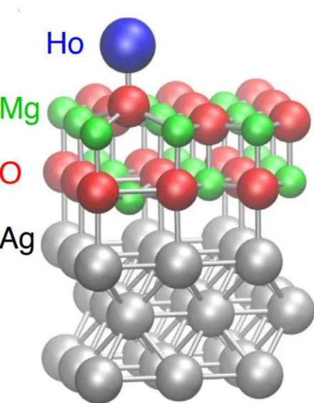
Model system: MgO on Ag(100)
Figure from: Donati et al. Science 352, 318 (2016)
top view
Science 352, 318 (2016)
What did we know about stable Ho magnets so far?
Prediction of a Ho moment of ~5.7µ
BOn 7 ML MgO
39
Measuring the Ho bit moment
ESR line only jumps after we deliberately switch the Ho atom
→Ho on MgO is a stable magnet
mHo = (10.1 ± 0.1) µB
F.D. Natterer et al., Nature 543, 226 (2017) f0 f↓
f↑
Δf = a mHomFe/r3
40
A two “Ho bit” memory
2 bit memory:
• Designed with dipole-dipole coupling to Fe sensor in mind
• read out via TMR and via Fe sensor
Fe (sensor)
Ho
SHo
F1 nm
y x
Ho
SHo
FF.D. Natterer et al., Nature 543, 226 (2017)
41
A four “Ho bit” memory
“multiplexing” allows reading of N bits simultaneously
Courtesy of William Paul
75 100 125 150 0.01
0.1 1 10
Switching rate (s-1 )
V (mV)
42
Tunnel Magnetoresistance on Ho
Magnetic Switching
0 20 40 60
24 25
I (pA)
Time (s)
10 100
0.01 0.1 1 10
Switching rate (s-1 )
I (pA)
Ho
Ho Fe
Ho
MgO/Ag(100) tip
Bz
I V
V = 150 mV I= 1.5 nA
V = 150 mV
Controlling the magnetic state
F.D. Natterer et al., Nature 543, 226 (2017)
IETS on magnetic atoms
Baumann et al., Phys. Rev. Lett. 115, 237202 (2015)
IETS on magnetic atoms
B=0T
Baumann et al., Phys. Rev. Lett. 115, 237202 (2015)
IETS on magnetic atoms
Baumann et al., Phys. Rev. Lett. 115, 237202 (2015) B=0T
B=4T
Instrumentation
• Vibrations
• Acoustic noise
• Low temperature
• Ultra-high vacuum
• RF cabling
• magnets
arXiv:1810.03887
47
IBM 1.2 K STM
48
-1000 -500 0 500 1000
0.0 0.5 1.0 1.5 2.0
dI/dV (normalized)
V (V)
Teff= 232 mK
ΔE = 3.3 kb T ≈ 70 µeV
Aluminum in a dilution refrigerator at 10 mK
Song et al. RSI 81, 121101 (2010)
Ultra low temperature STM
STM@EPFL
T
STM= 400 mK, B
zmax= ±8.5 T, B
vector= 0.8 T
Outlook: Atomic Details Matter
Stable Single Atom Magnet Paramagnetic Atom
Mgo Ho
How to access the individual magnets?
m
TiH= (1.004 ± 0.001) µ
BarXiv:1810.03887
Graphene Field Effect Device and Navigation
52 250 μm
MLG
BLG
SLG
1 nm
100 μm
5 μm
V
b53
Scanning Tunneling Microscopy on Graphene Devices
53
Empty States
Filled States
Tip DOS Graphene DOS
dI/dV
SiO2 h-BN
Graphene
V
gV
b- Scanning Tunneling Spectroscopy (STS)
• Density of state information
- Scanning Tunneling Microscopy (STM)
• Spatial information of samples
Tunneling current
E
DSiO2 h-BN
Graphene
V
gV
bGate Voltage as a Tuning Knob
54
dI /dV
dI /dV
dI /dV
E
DE
DE
DEF
EF EF
V
bV
bV
bHow to Compose a Spectroscopic “Gate Map” ?
55
-30 -20 -10 0 10 20 30 40
-300 -200 -100 0 100 200 300
Sample bias (mV)
Gate Voltage (V)
E
FdI/dV dI/dV
dI/dV
Unoccupied States
Occupied States
Color Coding dI/dV data for all Gate Voltages
56
-30 -20 -10 0 10 20 30 40
-300 -200 -100 0 100 200 300
Sample bias (mV)
Gate Voltage (V)
E
FdI/dV dI/dV
dI/dV
Unoccupied States
Occupied States
Fully Developed Gate Map with dI/dV data
57
E
FUnoccupied States
Occupied States
-30 -20 -10 0 10 20 30 40
-300 -200 -100 0 100 200 300
Sample bias (mV)
Gate Voltage (V)
Averaging only Helps with Noise…
58
-100 -50 0 50 100
-2 0 2
Vg=+45V L_42501
IETS signal
Bias (mV)
-100 -50 0 50 100
-2 -1 0 1 2
Vg=+25V L_42482
Bias (mV)
IETS, 3mVrms, 200ms, 135pts, SP: ±100mV/500pA (- for Vg<0)
11h 15h
Lots of Spectral Features…
59
-100 -50 0 50 100
-2 0 2
Vg=+45V L_42501
IETS signal
Bias (mV)
-100 -50 0 50 100
-2 -1 0 1 2
Vg=+25V L_42482
Bias (mV)
IETS, 3mVrms, 200ms, 135pts, SP: ±100mV/500pA (- for Vg<0)
Where are the phonons?
? ? ?
? ? ? ?
? ?
? ? ?
?
?
?
“There is no such thing as a free lunch.”
61
-30 -20 -10 0 10 20 30 40
-300 -200 -100 0 100 200 300
Sample bias (mV)
Gate Voltage (V)
condensing/averaging all spectra into one
The Bill:
no gate resolution
𝑑𝐼ൗ 𝑑𝑉
ℏω
𝑒𝑉
−ℏω
𝑑2𝐼ൗ
𝑑𝑉2
ℏω
−ℏω 𝑒𝑉
Inelastic excitations at constant threshold
ℏ𝜔
−ℏ𝜔
“There is no such thing as a free lunch.”
62
𝑑𝐼ൗ 𝑑𝑉
ℏω
𝑒𝑉
−ℏω
𝑑2𝐼ൗ
𝑑𝑉2
ℏω
−ℏω 𝑒𝑉
Inelastic excitations at constant threshold
Zoom into Exposed Excitations
63
Extracting threshold energies
How does it Compare to Phonon Dispersion and Density of States?
64
Excellent agreement with maxima in phonon DOS
ћ𝝎 IETS (meV) DFT (meV) Symmetry
1 56.8 ± 0.9 58 M3+
2 80.9 ± 1.3 78.1 M2±
3 152.8 ± 1.2 148.9 K5 4 176.9 ± 1.5 172.6 M3-
5 195 ± 2 198.7 Γ5+
6 359 ± 1 356.2 Γ5+ + K1
Flat dispersion→ large DOS
large electron-phonon coupling
Gate (Density) Resolved Phonon Spectroscopy
65
-40 -20 0 20 40
-500 -250 0 250 500
V b (mV)
Vg (V)
Natterer et al. Phys. Rev. Lett. 114, 245502 (2015) ℏ𝜔
1-2 1-2 3-5 6
3-5 6
We know where to look at:
Phonons appear as “faint” horizontal lines
ћ𝝎 IETS (meV) DFT (meV) Symmetry
1 56.8 ± 0.9 58 M3+
2 80.9 ± 1.3 78.1 M2±
3 152.8 ± 1.2 148.9 K5 4 176.9 ± 1.5 172.6 M3-
5 195 ± 2 198.7 Γ5+
6 359 ± 1 356.2 Γ5+ + K1
Phonon Intensities Show Asymmetries
66
Two asymmetries in phonon intensity:
• With respect to charge carrier concentration
• With respect to bias
-40 -20 0 20 40
-500 -250 0 250 500
V b (mV)
Vg (V)
-40 -20 0 20 40
-0.5 0.0 0.5 1.0
d2 I/dV2 (nS/V)-d2 I/dV2 (nS/V)
Vg (V)
-40 -20 0 20 40
-0.5 0.0 0.5 1.0
𝑉𝑏 = 359 meV
𝑉𝑏 = −359 meV
Natterer et al. Phys. Rev. Lett. 114, 245502 (2015)
Measuring Apparent Barrier Heights
• Current: 𝐼 𝑧 = 𝐼 0 𝑒 −2𝑎𝑧 , α = 5.1 Φ(𝑒𝑉)𝑛𝑚 −1
• 𝑑𝑙𝑛( ൗ
𝐼 𝐼0)
𝑑𝑧 = −2𝛼
• Φ = ℏ
28𝑚
𝑑𝑙𝑛( ൗ
𝐼 𝐼0) 𝑑𝑧
2
≈ 0.95 𝑑𝑙𝑛( ൗ
𝐼 𝐼0
) 𝑑𝑧
2
H 2 on h-BN/Ni(111)
Condensation around Ti atoms 3 × 3 𝑅30
°unit cell
5 nm 1 L H2, TD = 10 K, h-BN/Ni(111)
F. D. Natterer, F. Patthey, and H. Brune, Phys. Rev. Lett. 111, 175303 (2013)
Molecular Rotations
• Hydrogen dosing at 10 K
• 𝑇
𝑆𝑇𝑀= 4.7 K
10 Å
H
2Natterer et al., ACS nano 8, 7099 (2014)
Rotational Excitation Spectroscopy
𝑅g = 1 × 10⁹ Ω
F. D. Natterer, F. Patthey, and H. Brune, Phys. Rev. Lett. 111, 175303 (2013)
11% ≤ ∆𝜎 ൗ
𝜎 ≤ 37%
Scaling Behavior for Molecular Motion
𝑅g = 1 × 10⁹ Ω
Examining scaling of threshold
excitations with isotopic substitution
Vibrational Excitations:
➢ scale with √mass
-1Rotational Excitations:
➢ scale with mass
-1Stipe et al., Science 280, 1732 (1998)
C
2H
2C
2D
2STM - RES
F. D. Natterer, F. Patthey, and H. Brune, Phys. Rev. Lett. 111, 175303 (2013) See also Li et al. Phys. Rev. Lett. 111, 146102 (2013) for H2/Au(110)
Examining scaling of threshold
excitations with isotopic substitution
Vibrational Excitations:
➢ scale with √mass
-1Rotational Excitations:
➢ scale with mass
-1STM - RES
Examining scaling of threshold
excitations with isotopic substitution
Vibrational Excitations:
➢ scale with mass
-1Rotational Excitations:
➢ scale with mass
-1F. D. Natterer, F. Patthey, and H. Brune, Phys. Rev. Lett. 111, 175303 (2013) See also Li et al. Phys. Rev. Lett. 111, 146102 (2013) for H2/Au(110)
Rotational constant:
𝐵 = ℏ2ൗ 2𝐼
Homonuclear Diatomics
Ψ 𝑡𝑜𝑡 = Ψ 𝑒𝑙 Ψ 𝑣𝑖𝑏 Ψ 𝑛𝑢𝑐 Ψ 𝑟𝑜𝑡
𝐼𝑁 𝐼𝑁
Example: Hydrogen; nucleons are Fermions
Symmetric nuclear triplet state, 𝜳
𝒏𝒖𝒄➢ Antisymmetric rotational state, 𝜳
𝒓𝒐𝒕➢ Ortho-hydrogen
↑↑
(↓↓)
(↑↓+↓↑)/ 2
Antisymmetric singlet state, 𝜳
𝒏𝒖𝒄➢ Symmetric rotational state, 𝜳
𝒓𝒐𝒕➢ Para-hydrogen
(↑↓−↓↑)/ 2
are interdependent
→ Forbidden transition between ortho-para isomers
→ Molecules remain in their rotational subspace
Homonuclear Diatomics
Ψ 𝑡𝑜𝑡 = Ψ 𝑒𝑙 Ψ 𝑣𝑖𝑏 Ψ 𝑛𝑢𝑐 Ψ 𝑟𝑜𝑡
𝐼𝑁 𝐼𝑁
Example: Hydrogen; nucleons are Fermions
are interdependent
→ Forbidden transition between ortho-para isomers
→ Molecules remain in their rotational subspace
Energy Assignment in STM-RES
F. D. Natterer, F. Patthey, and H. Brune, Phys. Rev. Lett. 111, 175303 (2013) 76
➢ Excitations at 20.9±0.1, 32.8±0.4, and 43.8 ±0.1 meV are ∆𝐽 = 2 transitions of ortho-D
2, HD, and para-H
2➢ STM-RES energies equivalent to 3D rigid rotors in the gas phase
➢ Distinction of nuclear spin states Initial state ∆𝑱 = 𝟏 ∆𝑱 = 𝟐
p-H2 (𝐽 = 0) - 43.9 o-H2 (𝐽 = 1) - 72.8 o-D2 (𝐽 = 0) - 22.2 p-D2 (𝐽 = 1) - 36.9
HD (𝐽 = 0) 11.1 33.1
I. F. Silvera, Rev. Mod. Phys. 52, 393 (1980)