fields
Hiske Overweg, Hannah Eggimann, Anastasia Varlet, Marius Eich, Pauline Simonet, Yongjin Lee, Klaus Ensslin, and Thomas Ihn Solid State Physics Laboratory, ETH Z¨urich, CH-8093 Z¨urich, Switzerland
Ming-Hao Liu and Klaus Richter
Institut f¨ur Theoretische Physik, Universit¨at Regensburg, D-93040 Regensburg, Germany Kenji Watanabe and Takashi Taniguchi
Advanced Materials Laboratory, National Institute for Material Science, 1-1 Namiki, Tsukuba 305-0044, Japan Vladimir I. Fal’ko
National Graphene Institute, University of Manchester, Manchester M13 9PL, UK (Dated: December 23, 2016)
We report on the observation of magnetoresistance oscillations in graphenep-n junctions. The oscillations have been observed for six samples, consisting of single-layer and bilayer graphene, and persist up to temperatures of 30 K, where standard Shubnikov-de Haas oscillations are no longer discernible. We explain this phenomenon by the modulated densities of states in the n- andp- regions. A periodicity corresponding to a filling factor difference of 8 hints at a selection rule governing transitions between even and odd symmetry Landau levels.
The possibility to combine electron- and hole-like transport has led to the observation of a variety of in- teresting phenomena in graphenep-n junctions. In the absence of a magnetic field p-n junctions can give rise to Fabry-P´erot oscillations1–3, for which the oscillation period depends on the length of the cavity. In the pres- ence of an external magnetic fieldBperpendicular to the graphene plane this effect disappears when the cyclotron diameter becomes smaller than the characteristic length of the cavity. At low magnetic fields, in the range of B = 50 mT up to B = 2 T, depending on sample size and quality, snake states4,5 have been observed. Their periodicity is dictated by the length of thep-n interface.
In the quantum Hall regime the (partial) equilibration of edge channels6–10 and their shot noise11,12 have been studied.
We explore yet another phenomenon in graphene p-n junctions, in the magnetic field range below the onset of the quantum Hall effect. We observe magnetoresistance oscillations persisting up to temperatures as high as 30 K and occurring over a large density range. The oscil- latory pattern is the same for samples with one and two p-ninterfaces, monolayer and bilayer graphene, interface lengths ranging from 1 µm to 3 µm and is essentially particle-hole symmetric. The oscillations have been ob- served in a magnetic field range of B = 0.4 T up to B = 1.4 T. Their periodicity does not match the peri- odicity of the aforementioned snake states. In this paper we address this phenomenon and suggest a model which can quantitatively explain the oscillations.
Measurements were performed on six samples in to- tal, which all consist of a graphene flake encapsulated between two hexagonal boron nitride (h-BN) flakes on a Si/SiO2 substrate. They all show similar behavior. This
sample name A B C D E F
sample widthW (µm) 1.3 1.4 1.1 0.9 3 1.2 sample length L(µm) 3.0 1.4 1.0 2.3 3 2.8 top gate lengthLTG(µm) 1.1 0.7 0.55 1.2 1.0 1.0 distance to top gate(nm) 23 44 28 57 35 25 number of graphene layers 2 1 2 2 2 2
junction type npn pn npn pn npn npn TABLE I. Characteristics of samples A-F
paper focuses on measurements performed on one sam- ple (sample A), with the device geometry sketched in Fig. 1a. Specifications of the other five samples are sum- marized in table I. The bilayer graphene (BLG) flake was encapsulated with the dry transfer technique described in Ref. 13. A top gate was evaporated on the middle part of the sample, which divides the device into two outer regions, only gated by the back gate (single-gated re- gions), and the dual-gated middle region. The other five samples were made with the more recent van der Waals pick-up technique.14 Unless stated otherwise, the mea- surements were performed at 1.7 K. A constant voltage bias was applied symmetrically between the Ohmic con- tacts (‘source’ and ‘drain’ in Fig. 1a, inner contacts in Fig. 1b) and the current between the same contacts was measured. The transconductance dG/dVTG was mea- sured by applying an AC modulation voltage to the top gate.
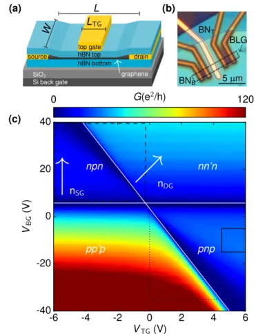
Figure 1c shows the conductance as a function of top gate voltage VTG and back gate voltage VBG. Charge neutrality of the single-gated regions shows up as a hori- zontal line of low conductance and is marked by a white line. The diagonal line of low conductance corresponds
arXiv:1612.07624v1 [cond-mat.mes-hall] 22 Dec 2016
to charge neutrality of the dual-gated region. The slope of this line is given by the capacitance ratio of the top and back gate. Together these lines divide the map into four regions with different combinations of carrier types:
two with the same polarities in the single- and dual-gated regions (pp’p andnn’n) and two with different polarities (npn and pnp). The conductance in the latter regions shows a modulation which is more clearly visible in the transconductance (see Fig. 2a). The oscillatory conduc- tance is caused by Fabry-P´erot interference of charge car- riers travelling back and forth in the region of the sample underneath the top gate. Their periodicity yields a cav- ity lengthLTG= 1.1µm, which is in agreement with the lithographic length of the top gate. The Fabry-P´erot os- cillations were studied in more detail in Ref. 3, which re- vealed the ballistic nature of transport in the dual-gated region.
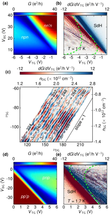
The Fabry-P´erot oscillations disappear in a magnetic field of B & 100 mT (see Fig. 2b-d). Yet at magnetic fields ofB = 0.4 T a new oscillatory pattern appears in thenpnandpnpregime. This can be seen in the conduc- tance and transconductance maps recorded atB= 0.5 T, shown in Figs. 3a,b,d,e. The oscillations follow neither the horizontal slope of features taking place in the single- gated region, nor the diagonal slope of the dual-gated region. They are therefore expected to occur at the in- terface between the p- and n-doped regions. This was confirmed by measurements on sample D, which had two contacts in the single-gated region and two contacts in the dual-gated region. For this sample, only the conduc- tance along paths involving the interface shows oscilla- tions.
On top of this novel oscillatory pattern the transcon- ductance of sample A in Fig. 3b(e) shows faint diagonal lines in the nn’n(pp’p) regime, which are Shubnikov-de Haas oscillations in the dual-gated region. The occur- rence of Shubnikov-de Haas oscillations shows that in this moderate magnetic field regime the Landau levels are broadened by disorder on the scale of their spacing, resulting in a modulation of the density of states.
Using a plate capacitor model described in the supple- mental material of Ref. 3, the gate voltage axes can be converted into density and filling factor axes, νX with X = SG,DG for the single- and dual-gated regions, re- spectively. The result of this transformation is shown in Fig. 3c. The oscillatory pattern has a slope of one, i.e. it follows lines of constant filling factor difference
∆ν =νSG−νDG. It appears that the oscillations can be described by:
G=hGi+A cos(2π∆ν
8 ) (1)
where A is the amplitude of the oscillations, which is on the order of 4 % of the background conductancehGi at T = 1.7 K. The distance between one conductance maximum and the next can therefore be bridged by ei- ther changing the filling factor in one region by 8, or by changing the filling factor in both regions by 4 oppositely.
(a) L
LTG
W
top gate hBN top hBN bottom
source drain
SiO2
Si back gate
graphene
←
(b)
BLG
← 5µm BNT
BNB
0 G(e2/h) 120
-6 -4 -2 0 2 4 6
VTG(V) -40
-20 0 20 40
VBG(V) (c)
nn’n npn
pp’p pnp
−→
nDG− →
nSG
FIG. 1. Characterization of the device. (a) Schematic of the device: a bilayer graphene flake is encapsulated between h- BN layers. It is contacted by Au contacts and a Au top gate is patterned on top, which defines the dual-gated region. (b) Optical microscope image of the sample. The four contacts, of which only the inner ones were used, appear orange. The top gate is outlined by a red curve. (c) Conductance of the sample at B = 0 T, T = 1.7 K. Four regions of different polarities are indicated. A zoom of the transconductance in the boxed region with a solid line is shown in Fig. 2. The dashed (dotted) box indicates the gate voltage range in which Figs. 3a,b (d,e) were measured.
It should be noted that Eq. (1) can be used to describe the oscillations in all six samples, regardless of the num- ber of graphene layers and the sample width (see table I).
The oscillations persist in magnetic fields up to B = 1 T for sample A and the periodicity scales with ∆ν for the entire magnetic field range. In higher magnetic fields the conductance is dominated by quantum Hall edge channels and takes on values below e2/h in the npn and pnp regimes, in agreement with observations by Amet et al.9
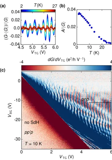
The oscillatory conductance is quite robust against temperature changes. Figure 4a,b show the decay of the amplitude as a function of temperature T. The oscilla- tory conductance in thepnpandnpnregime disappear at
-15 -10 -5
VBG(V) (a)
B= 0.0 T
(b)
B= 0.1 T
4.5 5 5.5 6
VTG(V) -15
-10 -5
VBG(V) (c)
B= 0.2 T
4.5 5 5.5 6
VTG(V) (d)
B= 0.3 T
-12 dG/dVTG(e2/h V−1) 12
FIG. 2. Disappearance of Fabry-P´erot oscillations with in- creasing magnetic field. The measurement was taken in the boxed region with solid lines in Fig. 1c. AtB = 0 T (a) the transconductance shows clear Fabry-P´erot oscillations. They disappear in a magnetic field ofB&0.1 T (b–d).
a temperature around 30 K. As can be seen in Fig. 4c, at T = 10 K the oscillations are still clearly present, while the Shubnikov-de Haas oscillations in the pp’p regime have already faded out.
The above discussed oscillations can be reproduced by transport calculations for an ideal SLG p-n junction at an intermediate magnetic field B, based on the scalable tight-binding model15. The ideal junction is modeled by connecting two semi-infinite graphene ribbons (oriented along armchair) with their carrier densities given by nL
in the far left andnRin the far right. A simple hyperbolic tangent function with smoothness 50 nm bridgingnLand nRis considered; see the inset of Fig. 5a for an example.
To cover the density range up to ±3×1012 cm−2 cor- responding to maximal Fermi energy of Emax≈0.2 eV, the scaling factor sf = 10 is chosen because it fulfills the scaling criterion15 sf 3t0π/Emax≈141 very well;
here t0 ≈ 3 eV is the hopping energy of the unscaled graphene lattice. Note that the following simulations considerW = 1µm for the width of the graphene ribbon, but simulations based on a different width show an iden- tical oscillation behavior (See Supporting Information for details), confirming its width-independent nature as al- ready concluded from our measurements.
The transmission function T(nR, nL) across the ideal p-njunction atB= 0.5 T is shown in Fig. 5a, where fine oscillations along symmetric bipolar axis (marked by the
0 40
G(e2/h)
-6 -5 -4 -3 -2 -1 VTG(V) 10
20 30 40
VBG(V)
nn’n npn
(a)
-12dG/dVTG(e2/h V−1)12
-6 -5 -4 -3 -2 -1 VTG(V) T = 1.7 K
SdH (b)
120 150 180 210
νDG
-100 -80 -60
νSG
slope
=1
∆ν=224
∆ν=232
∆ν=240
∆ν=248
∆ν=256
∆ν=264
∆ν=272
∆ν=280
∆ν=288
1.2 1.6nDG(×102.012cm−22.4) 2.8
-1.4 -1.2 -1.0 -0.8
nSG(×1012cm−2) -12 dG/dVTG(e2/h V−1) 12 (c)
0 G(e2/h) 40
0 1 2 3 4 5 6 VTG(V)
0 -10 -20 -30 VBG(V)
pp’p
pnp
(d) -12dG/dVTG(e2/h V−1)12
0 1 2 3 4 5 6 VTG(V)
SdH T = 1.7 K (e)
FIG. 3. Magnetotransport atB= 0.5 T. (a) Conductance of the sample at 0.5 T, showing an oscillatory pattern in thenpn regime. The measurement was taken in the dashed boxed re- gion of Fig. 1c. (b) The oscillatory pattern in thenpnregime is more clearly visible in the transconductance. Green dashed lines indicate the pattern expected for snake states. In the nn’n regime some faint lines can be distinguished, following the slope of the charge neutrality line of the dual gated region.
These are Shubnikov-de Haas oscillations. (c) Transconduc- tance atB= 0.5 T in thepnpregime as a function of charge carrier density (and filling factor) in the single- and dual- gated region. The oscillatory pattern follows the indicated line of slope one and can therefore be described by lines of constant filling factor difference ∆ν = νDG−νSG. (d),(e) Same as (a),(b), but with opposite charge carrier polarities.
The oscillations are essentially particle-hole symmetric.
2 T(K) 27
4.5 5.0 5.5 6.0 VTG(V) -0.04
-0.02 0.0 0.02 0.04
(G-hGi)/hGi
(a)
0 10 20
T (K) 0
0.02 0.04
A/hGi
(b)
-4 dG/dVTG(e2/h V−1) 4
0 2 4 6
VTG(V) -30
-20 -10 0
VBG(V) (c)
T = 10 K no SdH pp’p
pnp
FIG. 4. Temperature dependence. (a) Oscillatory part of the conductance as a function of top gate voltage and temperature measured along the line cut indicated by the black line in Fig. 4c. (b) Amplitude A of the oscillatory conductance as a function of temperature. The oscillations disappear around T = 30 K. (c) Transconductance atT = 10 K,B = 0.5 T in the pnp regime. Whereas Shubnikov-de Haas oscillations in thepp’p regime have faded out, the oscillatory pattern in the pnpregime persists.
blue arrows) from np to pn through the global charge neutrality point can be seen. Two regions marked by the white dashed boxes in Fig. 5a are zoomed-in and shown in Figs. 5b and d for a closer look and comparison with the measurements of sample B and E (Figs. 5c and e, respec- tively). Despite certain phase shifts (observed in Figs.
5b, d, and e) that are beyond the scope of the present study, good agreement between our transport simulation and experiment showing the oscillation period well ful- filling Eq. (1) can be seen.
Other works4,5 report on the formation of so called snake states along p-n interfaces in graphene. Snake states result in a minimum in the conductance whenever the sample widthW and the cyclotron radiusRc satisfy W/Rc = 4m−1 with m a positive integer. In the den- sity range of Fig. 3b,e this would lead to two resonances at most (indicated by green dashed lines in Fig. 3b,e),
which is far less than the observed number of resonances.
On top of that, snake states are inconsistent with the observed absence of a dependence on sample width. Fur- thermore, the tight-binding simulation also confirms that the observed effect is independent of the sample width and cannot be suppressed by introducing strong lattice defects in the vicinity of thep-njunction (see Supporting Information). We therefore rule out snaking trajectories as a possible cause of the observed oscillations.
Another process which could give rise to oscillations in a graphenep-n junction in a magnetic field is the inter- ference of charge carriers which are partly reflected and partly transmitted at the interface. When the charge car- rier densities are equal on both sides of the interface, elec- trons and holes will have equal cyclotron radii and there- fore the paths of transmitted and reflected charge carriers will form closed loops. For the case of equal density, this model predicts the right periodicity of the oscillations.16 Experimentally, however, the measured oscillations are still visible when the densities on both sides of thep-n interface are quite different: at the point (VBG,VTG) = (12,-6) V for example (see Fig. 3b), the cyclotron radii on thep andn side are respectively 0.36µm and 0.16 µm.
The path lengths hence differ by 2∆Rc= 0.40µm, which is more than seven times the Fermi wavelength (0.02µm and 0.05µm). It seems unlikely that interference between charge carriers on skipping orbits can still occur in this density regime. On top of that, the tight-binding simu- lations show that the oscillatory pattern is still present when introducing large-area lattice defects in the vicinity of thep-n junction, which destroy the skipping trajecto- ries (see Supporting Information). Thus the observed oscillations cannot be ascribed to interference of charge carriers on cyclotron orbits at thep-n interface.
Since the oscillations occur in both single-layer and bi- layer graphene, we exclude an explanation that relies on specific details of the dispersion relation. In the mag- netic field range where the oscillations are observed, the sample width is comparable to the classical cyclotron di- ameter. This excludes explanations based on classical electron flow following skipping orbit-like motion along edges.
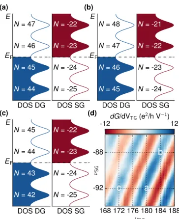
A mechanism which may cause the oscillations involves the alignment of the density of states (DOS) around the Fermi energy. Diagrams of the DOS in the single- and dual-gated regions are sketched in Figs. 6a-c. Figure 6d shows a zoom in the map of the oscillatory transcon- ductance of Fig. 3c. At pointa in this zoom the filling factor in the dual-gated regime isνDG= 180 andνSG= - 92 in the single-gated region. Because of the fourfold degeneracy of the Landau levels, Landau level numbers areN = 45 and N = -23 respectively, as shown in the DOS diagram of Fig. 6a. When following the oscilla- tory pattern from point a to point b, the two combs of DOS remain aligned with one another and only the Fermi level changes. This in contrast to what happens when moving from point a to point c: the DOSs shift with respect to one another and the transconductance oscil-
b d
-3 -2 -1 0 1 2 3
nR (1012 cm-2) -3
-2 -1 0 1 2 3
n L (1012 cm-2 ) 20
40 60 T
-200 0 200 x (nm) -10
1 2
n(x)
-180 -160 -140 -120 νR
140 160 180
ν L
25 30 35 40 45 T
-180 -160 -140 -120 νDG 140
160 180
ν SG
-12 0 12 G'
-140 -120 -100 -80 -60 -40 νR
60 80 100 120
10 20 30 T
-140 -120 -100 -80 -60 -40 νDG
60 80 100 120
-12 0 12 G' (a)
(b)
(c)
(d)
(e)
FIG. 5. (a) TransmissionT as a function of the carrier densities in the left,nL, and right,nR, for an ideal SLGp-n junction at a perpendicular magnetic fieldB= 0.5 T based on a tight-binding transport calculation (color range restricted for clarity).
Oscillations occur in the vicinity of the symmetric bipolar axis marked by blue arrows. Inset: an example of the considered carrier density profile corresponding to the white cross. White dashed boxes correspond to the density regions shown in panels (b) and (d), where the carrier density values are transformed in filling factors. (c)/(e) Transconductance G0 measured for sample B/E shown with the filling factor range same as (b)/(d).
lates. It could therefore be the case that the alignment of the DOS affects the conductance of thep-n interface in a way similar to the magneto-intersubband oscillations (MISO) of a two-dimensional electron gas (2DEG):17,18 the occupation of two energy subbands of a 2DEG can lead to enhanced scattering between the subbands when the DOSs of the subbands are aligned. A similar en- hancement of the coupling could occur in a graphenep-n junction. Just as for the oscillations we report on, MISO persist up to relatively high temperatures. The spacing predicted by this model lacks a factor of two compared to the experiment however: it would predict the argument of the cosine of Eq. (1) to be 2π∆ν/4. The explana- tion of the data requires the invocation of an even-odd asymmetry between the Landau levels to describe the measured periodicity: a coupling between Landau levels leading to higher/lower conductance when Landau levels of same/opposite parities are aligned, could account for the missing factor of two.
In conclusion, we have observed oscillations in the con- ductance of six graphene p-n junctions in the magnetic field range ofB= 0.4−1.5 T. The oscillations are inde- pendent of sample width and can be described by the fill- ing factor difference between the single- and dual-gated region. The oscillations are quite robust against tem- perature changes: they fade out only in the range of T = 20−40 K, whereas Shubnikov-de Haas oscillations decay belowT = 10 K. The oscillations can be well re- produced by tight-binding transport calculations consid- ering an ideal p-n junction at a constant magnetic field.
Up to a factor of two, the oscillatory pattern can be ex- plained by considering the density of states alignment of the single- and dual-gated regions.
ACKNOWLEDGEMENT
We thank P´eter Makk and Fran¸cois Peeters for fruit- ful discussions. We acknowledge financial support from the European Graphene Flagship and the Swiss National Science Foundation via NCCR Quantum Science and Technology. M.-H.L. and K.R. acknowledge financial support by the Deutsche Forschungsgemeinschaft within SFB 689.
DOS DG (a)
EF
E
N = 44 N = 45 N = 46 N = 47
DOS SG N = -25 N = -24 N = -23 N = -22
DOS DG (b)
EF
E
N= 45 N= 46 N= 47 N= 48
DOS SG N = -24 N = -23 N = -22 N = -21
DOS DG (c)
N = 42 N = 43 N = 44 N = 45
EF
E
DOS SG N = -25 N = -24 N = -23
N = -22 (d) -12dG/dVTG(e2/h V−1)12
168 172 176 180 184 188 νDG
-88
-92 νSG
a b
c
FIG. 6. (a-c) Schematics of the densities of states as a function of energy for the single- and dual-gated regions of the sam- ple at positions a-c of the measurement (d) Zoom in Fig. 3c.
The alignment of the densities of states can lead to an oscil- latory pattern with the right slope: along the line from point a to point b the two combs of densities of states stay aligned, whereas the combs shift with respect to one another when moving from point a to point c.
1 A. L. Grushina, D.-K. Ki, and A. F. Morpurgo, Applied Physics Letters102, 223102 (2013).
2 P. Rickhaus, R. Maurand, M.-H. Liu, M. Weiss, K. Richter, and C. Sch¨onenberger, Nature Communications 4, 2342 (2013).
3 A. Varlet, M.-H. Liu, V. Krueckl, D. Bischoff, P. Simonet, K. Watanabe, T. Taniguchi, K. Richter, K. Ensslin, and T. Ihn, Physical Review Letters113, 116601 (2014).
4 T. Taychatanapat, J. Y. Tan, Y. Yeo, K. Watanabe, T. Taniguchi, and B. ¨Ozyilmaz, Nature Communications 6, 6093 (2015).
5 P. Rickhaus, P. Makk, M.-H. Liu, E. T´ov´ari, M. Weiss, R. Maurand, K. Richter, and C. Sch¨onenberger, Nature Communications6, 6470 (2015).
6 J. R. Williams, L. Dicarlo, and C. M. Marcus, Science 317, 638 (2007).
7 B. ¨Ozyilmaz, P. Jarillo-Herrero, D. Efetov, D. A. Abanin, L. S. Levitov, and P. Kim, Physical Review Letters99, 2
(2007).
8 D. K. Ki, S. G. Nam, H. J. Lee, and B. ¨Ozyilmaz, Physical Review B81, 1 (2010).
9 F. Amet, J. R. Williams, K. Watanabe, T. Taniguchi, and D. Goldhaber-Gordon, Physical Review Letters112, 1 (2014).
10 E. T´ov´ari, P. Makk, P. Rickhaus, C. Sch¨onenberger, and S. Csonka, Nanoscale8, 11480 (2016).
11 N. Kumada, F. D. Parmentier, H. Hibino, D. C. Glattli, and P. Roulleau, Nature Communications6, 8068 (2015).
12 S. Matsuo, S. Takeshita, T. Tanaka, S. Nakaharai, K. Tsukagoshi, T. Moriyama, T. Ono, and K. Kobayashi, Nature Communications6, 8066 (2015).
13 C. R. Dean, A. F. Young, I. Meric, C. Lee, L. Wang, S. Sor- genfrei, K. Watanabe, T. Taniguchi, P. Kim, K. L. Shep- ard, and J. Hone, Nature Nanotechnology5, 722 (2010).
14 L. Wang, I. Meric, P. Y. Huang, Q. Gao, Y. Gao, H. Tran, T. Taniguchi, K. Watanabe, L. M. Campos, D. A. Muller,
J. Guo, P. Kim, J. Hone, K. L. Shepard, and C. R. Dean, Science342, 614 (2013).
15 M.-H. Liu, P. Rickhaus, P. Makk, E. T´ov´ari, R. Mau- rand, F. Tkatschenko, M. Weiss, C. Sch¨onenberger, and K. Richter, Physical Review Letters114, 1 (2015).
16 A. A. Patel, N. Davies, V. Cheianov, and V. I. Fal’ko, Physical Review B86, 1 (2012).
17 M. Raikh and T. Shahbazyan, Physical Review B49, 5531 (1994).
18 I. A. Dmitriev, A. D. Mirlin, D. G. Polyakov, and M. A.
Zudov, Reviews of Modern Physics84, 1709 (2012).
Oscillating Magnetoresistance in Graphene p-n Junctions at Intermediate Magnetic Felds
Hiske Overweg,1Hannah Eggimann,1Ming-Hao Liu,2Anastasia Varlet,1Marius Eich,1Pauline Simonet,1Yongjin Lee,1Kenji Watanabe,3Takashi Taniguchi,3Klaus Richter,2Vladimir I. Fal’ko,4Klaus Ensslin,1and Thomas Ihn1
1Solid State Physics Laboratory, ETH Z¨urich, CH-8093 Z¨urich, Switzerland
2Institut f¨ur Theoretische Physik, Universit¨at Regensburg, D-93040 Regensburg, Germany
3Advanced Materials Laboratory, National Institute for Material Science, 1-1 Namiki, Tsukuba 305-0044, Japan
4National Graphene Institute, University of Manchester, Manchester M13 9PL, UK (Dated: December 20, 2016)
Overview
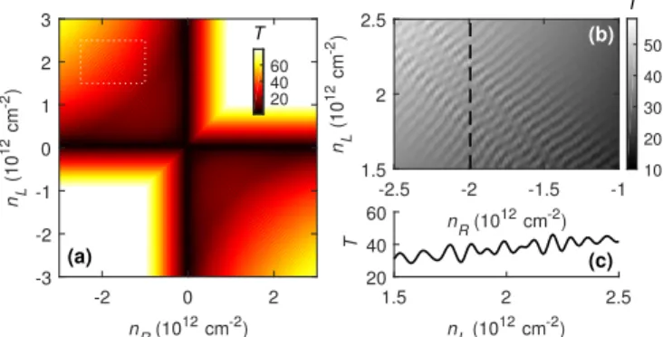
In the main text, we have shown a transmission map as a function of left and right carrier density, calculated using the real-space Green’s function method based on the scalable tight-binding model [1]. The considered graphene ribbon of widthW =1µm is subject to a model density function de- scribing an idealpnjunction with smoothness 50nm. The full map is repeated here in Fig.S1(a), with a white box marking the region plotted in Fig.S1(b).
In this Supporting Information, we show more numerical results in order to demonstrate that the observed oscillation is independent of the smoothness of thepnjunction and the width of the graphene ribbon, and is not related the current along thepnjunction. Instead, the oscillation is shown by the last numerical test to be closely related to the Landau levels away from thepnjunction.
For quantitative and systematic comparisons, we will focus on the density range shown in Fig.S1(b) and the line cut on it along the dashed line shown in Fig.S1(c). All calculations shown in the following consider the same density range and resolution as Figs.S1(b) and (c), which can be regarded as the reference panels of this Supporting Information. In particu- lar, the line cut of Fig.S1(c) will be repeatedly shown in the following results.
-2 0 2
nR (1012 cm-2) -3
-2 -1 0 1 2 3
nL (1012 cm-2) 2040
60 T
-2.5 -2 -1.5 -1
nR (1012 cm-2) 1.5
2 2.5
nL (1012 cm-2)
10 20 30 40 50 T
1.5 2 2.5
nL (1012 cm-2) 20
40 60
T(a)
(b)
(c)
FIG. S1. (a) Transmission mapT(nR,nL)same as Fig. 5(a) in the main text (smoothness 50nm and graphene widthW=1µm); white dashed box marks the region shown in (b), where a black dashed line indicates the line cut ofT(nL)at fixednR≈ −2×1012cm−2shown in (c).
-2.5 -2 -1.5 -1
nR (1012 cm-2) 1.5
2 2.5
nL (1012 cm-2)
20 40 60 T
1.5 2 2.5
nL (1012 cm-2) 20
40 60
T
(a) (b)
FIG. S2. (a) Transmission mapT(nR,nL)similar to Fig.S1(b) but with smoothness 25nm of thepnjunction. The red dashed line indi- cates the line cut shown as a red line in (b), where the black line is the reference line identical to Fig.S1(c) for the case with smoothness 50nm.
Smoothness dependence
Figure S2(a) presents the transmission map with smooth- ness of 25nm, showing a similar pattern seen in Fig.S1(b) where the junction smoothness is 50nm. A more quantitative comparison is shown in Fig.S2(b) for the line cuts of the two cases. Despite a slightly higherT obtained for the sharper junction due to the Klein collimation [2], i.e., the sharper the pnjunction, the wider the finite transmission probability of the angle distribution and hence the conductance, the gen- eral trend of the oscillation is shown to be independent of the smoothness.
In the rest of the numerical results, the smoothness will be fixed to 50nm.
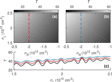
Width dependence
Figure S3 presents the transmission map based on a graphene ribbon withW =0.9µm shown in its panel (a) and W =0.8µm shown in its panel (b). Comparing the line cuts in Fig.S3(c), along with the reference line of Fig. S1(c) for the case ofW =1µm, the feature of the oscillation is clearly shown to be width-independent. On the other hand, the oscil- lation amplitude decreasing with the reduced graphene width implies that the oscillation may be closely related to the Lan- dau levels in the bulk away from thepnjunction, since the wider the graphene ribbon the better the Landau levels can develop.
-2.5 -2 -1.5 -1 nR (1012 cm-2) 1.5
2 2.5
n L (1012 cm-2)
20 40 60
T
-2.5 -2 -1.5 -1
nR (1012 cm-2)
20 40 60
T
1.5 2 2.5
nL (1012 cm-2) 20
40 60
T
(a) (b)
(c)
FIG. S3. Transmission mapsT(nR,nL)similar to Fig. S1(b) with the same smoothness of 50nm but with (a)W=0.9µm and (b)W= 0.8µm. Line cuts along the red/blue dashed line marked in (a)/(b) are compared in (c) together with the reference line (black) of Fig.S1(c) for the case ofW=1µm.
In the rest of the numerical results, the graphene width will be fixed asW=1µm.
Strong lattice defects
Next we show that the oscillation is not related to the cur- rent along thepnjunction. To this end, we consider large-area lattice defects located in the vicinity of thepnjunction. The basic idea is that if the oscillation came from any interference due to the current along thepn junction, such as the snake state [3], a large-area lattice defect at thepn interface or in the vicinity of it would act as a strong scatterer, destroying the interference and hence suppressing the oscillation. Contrarily, if the oscillation survives the introduced large defects, the cur- rent along thepnjunction will then be ruled out from possible origins of the oscillation.
We first consider a 50×400nm2defect in Figs.S4(a) and (b); the defect is placed in front of thepnjunction (at a dis- tance 150nm) in the former, and exactly on thepnjunction in the latter. Despite an additional modulating pattern observed in Fig. S4(a), the fine oscillation patterns remain visible in both cases. By increasing the defect area to 300×300nm2, the transmission map shown in Fig.S4(c) still exhibits the same oscillation pattern. A quantitative comparison of the line cuts summarized in Fig.S4(d) together with the reference line from Fig.S1(c) clearly shows that the oscillations observed in Figs.S4(a)–(c) belong to the same type as all those shown previously.
The fact that the strong defect introduced in the vicinity of the pnjunction cannot suppress the oscillation clearly indi- cates that any possible interference effect due to the current along thepnjunction cannot be the origin causing the oscilla- tion. Instead, the oscillation seems to depend only on the Lan-
-2.5 -2 -1.5 -1 nR (1012 cm-2) 1.5
2 2.5
nL (1012 cm-2)
15 20 25 30 T
-2.5 -2 -1.5 -1 nR (1012 cm-2) 10 15 20 25
T
-2.5 -2 -1.5 -1 nR (1012 cm-2) 15 20 25 30
T
1.5 2 2.5
nL (1012 cm-2) 0
50
T
(a) (b) (c)
(d)
FIG. S4. (a)–(c) Transmission mapsT(nR,nL)similar to Fig.S1(b) with the same smoothness of 50nm and widthW =1µm, but with a large-area defect represented by the black rectangle shown in the individual inset to the right of each panel, where the color back- ground depicts they-independent model functionn(x,y)describing the density variation of thepn junction. The size of the defect is 50×400nm2in (a,b) and 300×300nm2in (c). Line cuts along the red/blue/purple dashed line marked in (a)/(b)/(c) are compared in (d) together with the reference line (black) of Fig.S1(c) for the case without the defect.
dau levels that are well developed in the semi-infinite leads.
Fixed leads
So far, all the presented calculations are based on an infinite graphene ribbon with apnjunction in the middle, as described in the main text. Technically, this is achieved in numerics by considering a scattering region of sizeL×W attached to two leads from the left and right, both floating with the density profiles at the attaching edge of the scattering region. As long asLis much longer than the smoothness ofpnjunction (L= 400nm has been adopted in all the presented calculations), the density values at the left and right edges of the scattering region will saturate to a constant, and the entire open quantum system of the finite-size scattering region attached to the two floating semi-infinite leads will resemble an idealpnjunction in the middle of an infinitely long graphene ribbon, exhibiting anL-independent transmission behavior.
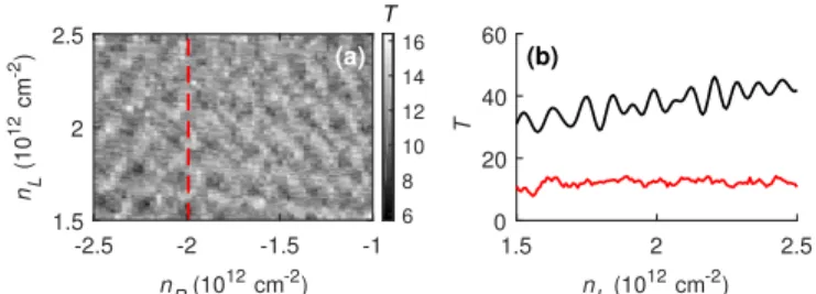
As a final and conclusive numerical test, we now fix the Fermi energies in the two semi-infinite leads at 0.1eV, and consider the same range and parameters as the reference panel of Fig. S1(b). The calculated transmission map is shown in Fig.S5(a), which no longer exhibits the fine oscillation.
The line cuts of fixed leads vs. floating leads compared in Fig.S5(b) clearly show that the oscillation completely van- ishes in the present case of fixed leads.
The vanishing oscillation is consistent with what we have speculated from the previously shown tests that the oscillation originates from the resonance between Landau levels well de- veloped in the far left and far right in the semi-infinite leads.
The present case shown in Fig.S5considers fixed Fermi ener-
-2.5 -2 -1.5 -1 nR (1012 cm-2) 1.5
2 2.5
nL (1012 cm-2)
6 8 10 12 14 16 T
1.5 2 2.5
nL (1012 cm-2) 0
20 40 60
T
(a) (b)
FIG. S5. (a) Transmission mapT(nR,nL)with the same range and parameters considered in Fig.S1(b) but with the two leads fixed at energyE=0.1eV. The red dashed line indicates the line cut shown as a red line in (b), where the black line is the reference line identical to Fig.S1(c) for the case with floating leads.
gies in the leads that no longer float with the densitiesnRand nL. Together with the fact that the lengthL=400nmW of the scattering region is too short for the Landau levels to form, the vanishing oscillation is therefore reasonably expected. By increasing the length of the scattering region to at leastL≈W, revival of the oscillation is expected for the case of fixed leads.
Note that the situation of fixed leads is actually closer to the
experiment, because the densities in graphene regions close to the contacts are rather pinned by the contact doping. However, the samples in our experiments (summarized in Table I in the main text) are long enough (several microns in all samples) for the Landau levels to develop well (with level spacing not far enough compared to disorder broadening in the magnetic field range we focus on) due to their cleanness and therefore exhibit the oscillation. Our numerical results based on floating leads correspond to the ideal case of infinitely long samples and therefore exhibit optimized oscillation.
[1] M.-H. Liu, P. Rickhaus, P. Makk, E. T´ov´ari, R. Maurand, F. Tkatschenko, M. Weiss, C. Sch¨onenberger, and K. Richter, Phys. Rev. Lett.114, 036601 (2015).
[2] V. V. Cheianov and V. I. Fal’ko,Phys. Rev. B74, 041403 (2006).
[3] P. Rickhaus, P. Makk, M.-H. Liu, E. T´ov´ari, M. Weiss, R. Mau- rand, K. Richter, and C. Sch¨onenberger,Nat. Commun.6, 6470 (2015).