Nuclear Instruments and Methods in Physics Research A 538 (2005) 384–407
Beam tests of ATLAS SCT silicon strip detector modules
F. Campabadal
a, C. Fleta
a, M. Key
a, M. Lozano
a, C. Martinez
a, G. Pellegrini
a, J.M. Rafi
a, M. Ullan
a, L. Johansen
b, B. Pommeresche
b, B. Stugu
b, A. Ciocio
c, V. Fadeyev
c, M. Gilchriese
c, C. Haber
c, J. Siegrist
c, H. Spieler
c, C. Vu
c, P.J. Bell
d,
D.G. Charlton
d, J.D. Dowell
d, B.J. Gallop
d, R.J. Homer
d, P. Jovanovic
d, G. Mahout
d, T.J. McMahon
d, J.A. Wilson
d, A.J. Barr
e, J.R. Carter
e, B.P. Fromant
e, M.J. Goodrick
e, J.C. Hill
e, C.G. Lester
e, M.J. Palmer
e, M.A. Parker
e, D. Robinson
e, A. Sabetfakhri
e, R.J. Shaw
e, F. Anghinolfi
f, E. Chesi
f, S. Chouridou
f, R. Fortin
f, J. Grosse-Knetter
f, M. Gruwe
f, P. Ferrari
f,
P. Jarron
f, J. Kaplon
f, A. Macpherson
f, T. Niinikoski
f, H. Pernegger
f, S. Roe
f, A. Rudge
f, G. Ruggiero
f, R. Wallny
f, P. Weilhammer
f, W. Bialas
g, W. Dabrowski
g, P. Grybos
g, S. Koperny
g, J. Blocki
h, P. Bruckman
h, S. Gadomski
h, J. Godlewski
h, E. Gornicki
h, P. Malecki
h, A. Moszczynski
h, E. Stanecka
h, M. Stodulski
h, R. Szczygiel
h, M. Turala
h, M. Wolter
h, A. Ahmad
i,
J. Benes
i, C. Carpentieri
i, L. Feld
i, C. Ketterer
i, J. Ludwig
i, J. Meinhardt
i, K. Runge
i, B. Mikulec
j, M. Mangin-Brinet
j, M. D’Onofrio
j, M. Donega
j, S. Moeˆd
j, A. Sfyrla
j, D. Ferrere
j, A.G. Clark
j, E. Perrin
j, M. Weber
j, R.L. Bates
k,
A. Cheplakov
k, D.H. Saxon
k, V. O’Shea
k, K.M. Smith
k, Y. Iwata
l, T. Ohsugi
l, T. Kohriki
m, T. Kondo
m, S. Terada
m, N. Ujiie
m, Y. Ikegami
m, Y. Unno
m, R. Takashima
n, T. Brodbeck
o, A. Chilingarov
o, G. Hughes
o, P. Ratoff
o, T. Sloan
o, P.P. Allport
p, G.-L. Casse
p, A. Greenall
p, J.N. Jackson
p, T.J. Jones
p, B.T. King
p,
S.J. Maxfield
p, N.A. Smith
p, P. Sutcliffe
p, J. Vossebeld
p, G.A. Beck
q, A.A. Carter
q, S.L. Lloyd
q, A.J. Martin
q, J. Morris
q, J. Morin
q, K. Nagai
q, T.W. Pritchard
q, B.E. Anderson
r, J.M. Butterworth
r, T.J. Fraser
r, T.W. Jones
r,
J.B. Lane
r, M. Postranecky
r, M.R.M. Warren
r, V. Cindro
s, G. Kramberger
s, I. Mandic´
s, M. Mikuzˇ
s, I.P. Duerdoth
t, J. Freestone
t, J.M. Foster
t, M. Ibbotson
t,
F.K. Loebinger
t, J. Pater
t, S.W. Snow
t, R.J. Thompson
t, T.M. Atkinson
u,
www.elsevier.com/locate/nima
0168-9002/$ - see front matterr2004 Elsevier B.V. All rights reserved.
doi:10.1016/j.nima.2004.08.133
Corresponding author. School of Physics, University of Melbourne, Victoria 3010, Australia.
E-mail address:gareth.moorhead@cern.ch (G.F. Moorhead).
G. Bright
u, S. Kazi
u, S. Lindsay
u, G.F. Moorhead
u,, G.N. Taylor
u,
G. Bachindgagyan
v, N. Baranova
v, D. Karmanov
v, M. Merkine
v, L. Andricek
w, S. Bethke
w, J. Kudlaty
w, G. Lutz
w, H.-G. Moser
w, R. Nisius
w, R. Richter
w, J. Schieck
w, T. Cornelissen
x, G.W. Gorfine
x, F.G. Hartjes
x, N.P. Hessey
x, P. de
Jong
x, A.J.M. Muijs
x, S.J.M. Peeters
x, Y. Tomeda
y, R. Tanaka
y, I. Nakano
y, O. Dorholt
z, K.M. Danielsen
z, T. Huse
z, H. Sandaker
z, S. Stapnes
z, P. Bargassaa
aa, A. Reichold
aa, T. Huffman
aa, R. Nickerson
aa, A. Weidberg
aa,
G. Doucas
aa, B. Hawes
aa, W. Lau
aa, D. Howell
aa, N. Kundu
aa, R. Wastie
aa, J. Bohm
bb, M. Mikestikova
bb, J. Stastny
bb, Z. Broklova´
cc, J. Brozˇ
cc, Z. Dolezˇal
cc,
P. Kodysˇ
cc, P. Kubı´k
cc, P. Rˇeznı´cˇek
cc, V. Vorobel
cc, I. Wilhelm
cc, D. Chren
dd, T. Horazdovsky
dd, V. Linhart
dd, S. Pospisil
dd, M. Sinor
dd, M. Solar
dd, B. Sopko
dd,
I. Stekl
dd, E.N. Ardashev
ee, S.N. Golovnya
ee, S.A. Gorokhov
ee, A.G. Kholodenko
ee, R.E. Rudenko
ee, V.N. Ryadovikov
ee, A.P. Vorobiev
ee,
P.J. Adkin
ff, R.J. Apsimon
ff, L.E. Batchelor
ff, J.P. Bizzell
ff, P. Booker
ff, V.R. Davis
ff, J.M. Easton
ff, C. Fowler
ff, M.D. Gibson
ff, S.J. Haywood
ff, C. MacWaters
ff, J.P. Matheson
ff, R.M. Matson
ff, S.J. McMahon
ff, F.S. Morris
ff,
M. Morrissey
ff, W.J. Murray
ff, P.W. Phillips
ff, M. Tyndel
ff, E.G. Villani
ff, D.E. Dorfan
gg, A.A. Grillo
gg, F. Rosenbaum
gg, H.F.-W. Sadrozinski
gg, A. Seiden
gg, E. Spencer
gg, M. Wilder
gg, P. Booth
hh, C.M. Buttar
hh, I. Dawson
hh, P. Dervan
hh, C. Grigson
hh, R. Harper
hh, A. Moraes
hh, L.S. Peak
ii, K.E. Varvell
ii,
Ming-Lee Chu
jj, Li-Shing Hou
jj, Shih-Chang Lee
jj, Ping-Kun Teng
jj, Changchun Wan
jj, K. Hara
kk, Y. Kato
kk, T. Kuwano
kk, M. Minagawa
kk, H. Sengoku
kk, N. Bingefors
ll, R. Brenner
ll, T. Ekelo¨f
ll, L. Eklund
ll, J. Bernabeu
mm,
J.V. Civera
mm, M.J. Costa
mm, J. Fuster
mm, C. Garcia
mm, J.E. Garcia
mm, S. Gonzalez-Sevilla
mm, C. Lacasta
mm, G. Llosa
mm, S. Marti-Garcia
mm, P. Modesto
mm, J. Sanchez
mm, L. Sospedra
mm, M. Vos
mm, D. Fasching
nn,
S. Gonzalez
nn, R.C. Jared
nn, E. Charles
nnaInstituto de Microelectronica de Barcelona, IMB-CNM, CSIC, Barcelona, Spain
bUniversity of Bergen, Bergen, Norway
cLawrence Berkeley Laboratory and University of California, Berkeley, CA, USA
dSchool of Physics and Astronomy, The University of Birmingham, Birmingham, UK
eCavendish Laboratory, Cambridge University, Cambridge, UK
fEuropean Laboratory for Particle Physics (CERN), Geneva, Switzerland
gFaculty of Physics and Nuclear Techniques, AGH University of Science and Technology, Cracow, Poland
hThe Henryk Niewodniczanski Institute of Nuclear Physics, Polish Academy of Sciences, Cracow, Poland
iFakulta¨t fu¨r Physik, Albert-Ludwigs-Universita¨t, Freiburg, Germany
jSection de Physique, Universite de Geneve, Switzerland
kDepartment of Physics and Astronomy, University of Glasgow, Glasgow, UK
lDepartment of Physics, Hiroshima University, Higashi-Hiroshima, Japan
mInstitute of Particles and Nuclear Studies (IPNS), KEK, Tsukuba, Japan
nKyoto University of Education, Fukakusa, Japan
oDepartment of Physics, Lancaster University, Lancaster, UK
pDepartment of Physics, Oliver Lodge Laboratory, University of Liverpool, Liverpool, UK
qDepartment of Physics, Queen Mary and Westfield College, University of London, London, UK
rDepartment of Physics and Astronomy, University College London, London, UK
sJ. Stefan Institute and Department of Physics, University of Ljubljana, Ljubljana, Slovenia
tDepartment of Physics and Astronomy, University of Manchester, Manchester, UK
uUniversity of Melbourne, Parkville, Victoria 3052, Australia
vMoscow State University, Moscow, Russia
wMax-Planck-Institut fu¨r Physik, Mu¨nchen, Germany
xNIKHEF, Amsterdam, The Netherlands
yPhysics Department, Okayama University, Okayama, Japan
zUniversity of Oslo, Oslo, Norway
aaDepartment of Physics, Oxford University, Oxford, UK
bbAcademy of Sciences of the Czech Republic (ASCR), Prague, Czech Republic
ccCharles University, Prague, Czech Republic
ddCzech Technical University, Prague, Czech Republic
eeInstitute of High Energy Physics (IHEP), Protvino, Russia
ffRutherford Appleton Laboratory, Chilton, Didcot, UK
ggSanta Cruz Institute for Particle Physics, University of California, Santa Cruz, California, USA
hhDepartment of Physics, University of Sheffield, Sheffield, UK
iiUniversity of Sydney, Sydney, Australia
jjInstitute of Physics, Academia Sinica, Taipei, Taiwan
kkInstitute of Physics, University of Tsukuba, Tsukuba, Japan
llUppsala University, Department of Radiation Sciences, Uppsala, Sweden
mmInstituto de Fisica Corpuscular (IFIC), Universidad de Valencia-CSIC, Valencia, Spain
nnDepartment of Physics, University of Wisconsin, Madison, Wisconsin, USA
Received 18 August 2004; accepted 31 August 2004 The ATLAS Semiconductor Tracker Collaboration
Available online 14 October 2004
Abstract
The design and technology of the silicon strip detector modules for the Semiconductor Tracker (SCT) of the ATLAS experiment have been finalised in the last several years. Integral to this process has been the measurement and verification of the tracking performance of the different module types in test beams at the CERN SPS and the KEK PS.
Tests have been performed to explore the module performance under various operating conditions including detector bias voltage, magnetic field, incidence angle, and state of irradiation up to 31014 protons per square centimetre. A particular emphasis has been the understanding of the operational consequences of the binary readout scheme.
r2004 Elsevier B.V. All rights reserved.
PACS:29.40
Keywords:ATLAS; Silicon; Micro-strip; Detector; Beam; Test
1. Introduction
The Semiconductor Tracker (SCT) will form the intermediate layers of the ATLAS [1] and Inner Detector[2]. It will provide four three-dimensional space-points on tracks at radial distances1 in the
range 27–56 cm. Good spatial resolution is required to provide a precise transverse momentum measure- ment in the bending direction of the 2 T magnetic field of the Inner Detector solenoid. The SCT consists of a central barrel consisting of four cylinders and two endcaps each consisting of nine
1The ATLAS geometry is best described in terms of a cylindrical coordinate system with its origin at the interaction
(footnote continued)
point and itsz-axis parallel to the beam line.
disks, covering a rapidity range up tojZjo2:5 with a half-length of 279 cm. The four barrel layers are 149 cm long covering the rapidity range up to jZjo1:0 with a transition to the endcaps byjZjo1:5:
The barrel and endcaps are populated with a total of 4088 silicon micro-strip detector modules.
The modules are constructed from two pairs of micro-strip sensors glued back-to-back with a 40 mrad stereo-angle providing a two-dimensional measurement. The sensors of the barrel modules are rectangular with strips nearly parallel to the beam axis. The endcap sensors are fan-shaped with strips nearly radial away from the beam axis. In both of these geometries the azimuthal angle f—
essential to the transverse momentum determina- tion—is measured with high precision. The barrel modules also provide a measurement with limited resolution in the coordinatezalong the beam axis, and the endcap modules in the radial distance R from the beam axis. In both cases the third coordinate is given by the sensor position. The barrel modules are all identical whereas the radial coverage of the endcaps requires three geometri- cally different versions[3,4].
All the silicon sensors are of 285mm thick n-type h1 1 1i material with a resistivity of 4–8 kOcm:
Each sensor has 768 active micro-strips formed by implanting pþ material. The strips on the barrel sensors have a pitch of 80mm;while the strip pitch on endcap modules varies from 54.4 to 94:8mm with the fan geometry. A detailed description of the sensors is given in Ref.[5].
The pþ implant is AC coupled to a metallized strip on the sensor surface which is connected to a channel of the readout electronics. The SCT front- end integrated circuit—the radiation-hard ABCD3T [6]—has 128 channels, and there are six chips on each side of the module. Each channel has preamplifier and shaper stages with a total shaping time of 20 ns. The SCT readout is binary: the amplified signal is discriminated on the chip, after which only one bit (on/off) of digital information remains. The digital information from all channels is sampled at the LHC clock frequency of 40 MHz and remains in a 128 bit wide pipeline on the chip during the trigger latency period of 3:2ms: On receipt of a level one accept (L1A), the hit pattern in the relevant pipeline cell is
shifted into an output buffer, compressed, and despatched serially to the data acquisition system.
The tracking performance of the SCT modules has been measured systematically in beam tests throughout their development. In this article we summarise beam measurements over the last several years during the final stages of develop- ment and qualification. These measurements have typically occurred several times a year at the H8 beamline of the Super Proton Synchrotron (SPS) at CERN. In 1999 and 2000, additional tests were carried out at the p2 beamline at the 12 GeV Proton Synchrotron at KEK. In the H8 beamline several secondary beam types and energies are available, the most commonly used for this work being 180 GeV charged pions. In the KEK tests a 3–4 GeV pion beam was used.
Modules are tested in the H8 beamline in batches of 10–12, mounted in-line along the beam axis. Modules of all four SCT geometries are tested together. The modules are contained in individual test boxes to simplify safe mounting and cooling, and surrounded by a common environ- mental enclosure. Extraneous material in the beamline is minimised. A separate set of silicon micro-strip detectors is used to provide reference tracking. A pair of scintillation counters provide a fast trigger signal which is delayed to the pipeline length of the SCT modules.
A beam test typically consists of a large number of short runs during which the front-end discrimi- nator threshold is scanned in steps through the expected signal range, resulting in an efficiency ‘‘s- curve’’ from which the collected charge distribu- tion can be recovered. The 12 or 16 runs of the threshold scan are repeated for each combination of the operating parameters of interest such as the silicon sensor bias voltage, the applied magnetic field, the angle of incidence on the silicon, the trigger timing, the position of the beam around the module, and the operating modes of the ABCD3T.
The effect of a strong magnetic field is tested by inserting the complete setup in the superconduct- ing 1.56 T Morpurgo magnet. This magnet pro- vides a vertical field over a volume large enough to contain the entire assembly. The modules are mounted with strips parallel to the field and normal to the incident beam, emulating the
configuration of barrel modules atZ¼0 inside the 2 T Inner Detector solenoid. The deviation of the charge carriers due to the Lorentz effect has been studied in detail yielding a precise measurement of the Lorentz angle.
A major design concern for the SCT is radiation tolerance during the lifetime of the experiment in the LHC. Modules have been systematically irradiated at the T7 proton irradiation facility at the CERN Proton Synchrotron [7–9] to fluences up to 31014protons=cm2;well in excess of that expected in 10 years of LHC operation. The performance of most of these irradiated modules was then studied extensively in the beam test program.
Recent testbeam results have been published in internal notes and conference proceedings[10–17].
Results from test beams prior to 1999 can be found in Refs.[18–22]. In this article, we describe the experimental set-up (Section 2), the offline analysis including the definition of the most important single-module tracking performance characteristics (Section 3), and the main results (Section 4.)
2. Set-up
The CERN 400–450 GeV SPS provides second- ary beams to the H8 beamline. The usual beam for SCT tests is 180 GeVpþ with a small fraction of mþ: Particles are extracted into the beamline during a spill of several seconds in a repeating cycle some 14–17 s long.2The intensity is roughly constant during the spill. The beam is parallel through the length of the assembly, and is about one centimetre in diameter.
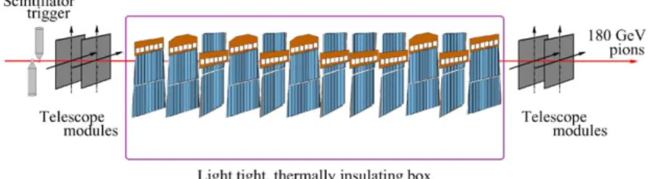
A typical arrangement, that of August 2002, is illustrated in Fig. 1 consisting of a scintillator trigger, a beam telescope and environment cham- ber containing the modules under test. The telescope and modules under test are mounted on
a granite table sitting on a trolley on a set of rails permitting insertion into the active volume of the magnet.
2.1. Trigger and timing
Two scintillator detectors sensed by photo- multiplier tubes are used to detect the passage of beam particles and trigger the readout system. The trigger signal timing jitter is around 1–2 ns. The acceptance of the scintillators is 22 cm2; large enough to contain typical beam spots and compar- able in size to the acceptance of the beam telescope. As the SCT modules have a sensitive area around 612 cm2 only a small region is tested at any one position of the module in the beam.
In ATLAS the readout of the detectors will be synchronised with the bunch crossings of the LHC. The SCT timing will be carefully optimised to ensure that the signal is sampled at the peak of the charge response curve. In most test beams, however, the beam and readout clock are not synchronised.3 The beam particles and therefore the trigger signal arrive with random phase with respect to the 40 MHz readout clock. Since electronics designed for the LHC has typically a short rise-time comparable to the 25 ns clock period, this random arrival time would have a severe effect on the apparent performance. There- fore the time between the raw trigger from the scintillators and the next rising edge of the clock is measured using a Time to Digital Converter (TDC),4 allowing the dependence of the perfor- mance on trigger phase to be evaluated off-line.
2.2. Beam telescope
A beam telescope is used to measure the trajectories of beam particles independently of the devices under test. The telescope modules consist of two perpendicular silicon micro-strip
2In recent years the SPS has been operated at 400 GeV. This reduced energy has allowed the total cycle length to be increased from 14.4 to 16.8 s with the spill increased from 2.58 to around 4.8 s, significantly reducing the integrated dead time between spills.
3In certain periods the SPS has been operated with an ‘‘LHC- like’’ bunch structure which has been used to test SCT modules under more stringent timing conditions. In this case the readout clock was synchronised to the accelerator RF bunches using the LHC timing distribution system.
4CAEN model V488.
sensors providing an X–Y space point. The sensors have a strip pitch of 50mm and are read out by VA2 analogue multiplexer chips with a peaking time of around 1ms: The modules are rigidly mounted on the same massive granite table as the modules under test, two before and two after the environment chamber. A spatial resolution better than 5mm is obtained. The analogue signal is digitised by flash ADC VME modules which also perform pedestal subtraction and cluster finding using on-board DSPs, significantly reducing the data volume. The dead time of this system, 13 ms, is the dominant limitation to the total event rate.
While the beam telescope provides a track with good spatial resolution compared to the SCT modules under test, it does so with a much longer shaping time. In order to ensure that a track detected in the telescope corresponds in time with the much shorter sensitive time window of the SCT modules, one of the SCT modules is also used to provide a reference hit. This ‘‘anchor’’ module does not undergo threshold or bias scans but is kept at constant settings selected for high effi- ciency and low noise occupancy. The requirement that the anchor module records a hit matching the telescope track also effectively eliminates residual inefficiencies due to clock and readout glitches, and since it is located among the modules under test, helps eliminate badly reconstructed or widely scattered tracks.
2.3. Control, readout and power supply
The SCT modules are powered, controlled and read out during the test beam measurements by a suite of custom VME cards which has been
developed specifically for small-scale SCT test systems[23–26].
A clock and control card (CLOAC) provides a common 40 MHz system clock to all detector modules and to the readout system. It is also used to distribute ‘‘fast’’ commands—resets and trig- gers—which are simultaneously transmitted to all modules during active data-taking, thus providing the global synchronisation. An important function of the CLOAC is to delay the prompt trigger signal by an amount equal to the pipeline length less any cable and gate delays, and then to issue a level-one accept synchronised to the next clock edge.
Slow command generator cards (SLOG) are used to assemble the long bit strings unique to each module which configure the many registers of the 12 ABCD3T chips. These ‘‘slow’’ commands are transmitted outside active data-taking. The SLOG modules also fan-out the clock and the fast commands to the individual modules, six modules per unit.
‘‘MuSTARD’’ cards receive the serial bit stream output data from the modules. Each MuSTARD reads out the two data links of six modules, 12 links in total. It performs header and trailer detection, making individual event data available over VME to the data acquisition system. It also provides fast on-board hit pattern decoding and occupancy histogramming with error detection.
In ATLAS the clock, command and data signals to and from the SCT will be carried by optical fibres. However, in the beam tests, optical readout has not been used. Instead, the LVDS electrical signals on the module are buffered nearby and transmitted by 25 m shielded twisted-pair cables to the control room.
Fig. 1. Arrangement of SCT prototype modules in the H8 beamline during the August 2002 beam test.
SCT low voltage VME cards (SCTLV3) provide the high-current analogue and digital power to the front-end chips on the modules as well as several low-current control voltage and temperature monitoring channels. The high-current voltage levels are compensated for ohmic voltage drops on the cable by a four-wire sensing scheme. Each SCTLV3 powers two modules.
SCT high voltage VME cards (SCTHV) provide the silicon detector bias voltage, up to 500 V at 5 mA, extreme values which may be required after high radiation doses. Each SCTHV supplies four modules.
2.4. Module calibration
A full characterisation of the module front-end parameters such as gain and noise is made in situ prior to the beam test using the ABCD3T’s in-built calibration circuit [6]. A voltage step across the calibration capacitor (Ccal) results in accumulated charge being injected into the front-end of the chip. The amplitude of the calibration charge is controlled by a DAC which can be configured through the range 0–13 fC. The response to the calibration charge is obtained by scanning the discriminator threshold, resulting in an occupancy
‘‘S-curve’’ histogram for each channel. A comple- mentary error function is fitted to this histogram yielding the median 50% point efficiencyðvt50Þand from the Gaussian spread the output noise. This process is repeated for several calibration charge amplitude settings from 0.5 to 8 fC covering the expected signal range. The graph ofvt50 threshold settings versus calibration charge amplitude de- scribes the response of each channel. The response is summarised at 2.0 fC by the gain, determined from the slope, the offset from the intercept, and the input noise determined by dividing the output noise by the gain.
The discriminator threshold setting is common to all channels within one chip. Any spread in the response among the different channels of a chip results in a spread of the efficiency and noise occupancy which degrades effective performance, particularly after irradiation. The ABCD3T has therefore been designed with threshold trim adjustments for each channel to allow the spread
to be minimised. This is a lengthy procedure which must be carried out before the final response can be measured.
In addition to the standard electrical procedure described above, further optimisation is required for irradiated modules as described in Ref. [27].
Modelled as a transimpedance amplifier with a bipolar input transistor, the front-end circuit of unirradiated ASICs have nominal values for collector (pre-amplifier) and shaper currents of 220 and 30mA; respectively. As a consequence of the b factor degradation, the optimum values of these currents decrease with irradiation. Two 5-bit DACs are therefore implemented in the ABCD3T to adjust the pre-amplifier and shaper currents[6].
Each chip is independently optimised. Typical values for irradiated modules are around 120 or 140mA for the input transistor current and 27 or 30 mA for the shaper bias. In 2002, beam tests of irradiated modules with different current config- urations were performed to study the variation of signal-to-noise with respect to pre-amplifier and shaper current.
Digital timing performance has also been observed to degrade with irradiation. It has been found that the number of slow channels can be significantly reduced by increasing the analogue voltage, Vcc; supplied to the chips. Set-up effects such as these are avoided by running the final response curve calibration in situ under the same conditions as for the beam measurements. For example, the temperature differences of the chips may also have a 5% effect on the noise measure- ment [28].
2.5. Cooling
The modules under test are mounted in a light- tight, thermally insulating chamber. The chamber is flushed with cold nitrogen gas to ensure a dry atmosphere. Each of the modules is contained in its own aluminium test box to which it is thermally coupled through its designed cooling contact surfaces. The test boxes, of various designs according to the particular module type, are cooled by water/ethanol chilled to around 15C:Each module dissipates up to 7 W power.
The resulting temperatures, measured by thermis-
tors mounted on the electronics hybrid of the module, are monitored continuously. Hybrid temperatures range between 5 and 5C: The detector leakage current of heavily irradiated detectors is in the range from 1 to 3 mA, depending on the cooling which is not as efficient as expected in ATLAS. Non-irradiated modules have currents of the order of 1mA:
3. Off-line and analysis
During the beam test, data from all sub- systems—telescope modules, SCT binary modules, TDC—are assembled into events and written to data files. To facilitate the analysis, these raw data are processed off-line into summary files. These present the data in an easily accessible n-tuple format. Off-line processing includes the internal alignment of telescope and module planes and the reconstruction of tracks using the measurements of the beam telescope.
3.1. Alignment
The beam telescope provides four very precise measurements in two perpendicular space coordi- nates. The reconstruction of the track and the interpolation to the plane of the module under test require a precise knowledge of the relative align- ment of all detectors in the set-up.
The positions of telescope and SCT modules, though stable, are only approximately fixed by the mounting frames. A precision measurement of the relative alignment of all planes is obtained using the tracks in a large number ð10,000) of events.
The alignment procedure minimises the alignment error by iteratively varying the alignment para- meters.
As a first step in the alignment procedure, the position of the global telescope frame is fixed by identifying X- and Y-axis with, respectively, the horizontal and vertical coordinates measured by the first telescope module, and theZ-axis with the beam direction. Once the global system is defined, the remaining telescope detectors are aligned by minimising the distance of their hits to tracks reconstructed from the outer two modules. At this
stage only two space points are used to define a track. Ambiguities due to noise hits are effectively avoided by rejecting events in which all four planes under consideration do not have exactly one hit.
After the internal alignment of the telescope, full three or four space point information from the telescope can be used to reconstruct tracks projected through the modules under test. The alignment parameters of each of the two planes of the test modules are varied until the difference between the interpolated track position and the measurement by the plane converges to a mini- mum. The two planes of each module are aligned independently.
When a magnetic field is applied, the tracks have a significant curvature. Moreover, the Lorentz effect leads to a displaced position measurement.
For data taken in the magnetic field the alignment procedure described above—with straight tracks—
is nevertheless applied. The effects of the magnetic field are thereby absorbed in the effective module positions. This procedure allows the interpolation of the track to the modules because all tracks have closely the same momentum.
The alignment procedure was repeated each time the set-up is physically accessed or whenever the magnetic field is changed.
3.2. Track reconstruction
The off-line pre-processing of the data includes the reconstruction of the tracks using the space points measured by the telescope.
The measurements of the two perpendicular planes of each telescope module are combined into three-dimensional space points. Track segments are constructed by combining the space points from the most upstream and most downstream modules. The track is then refined by including the space points from the intermediate telescope modules if the distance between the track and the space point is within 50mm:Events are included if the track contains at least three space points after this cut.
A number of track quality indicators are available to select a sample of tracks with a predefined efficiency and purity. The most im- portant are: the number of space points in the
track fit, thew2 of the fit, the track gradients with respect to the beam axis, and whether a hit is recorded in the anchor module. In the H8 beam tests the position where the tracks are incident on each module is interpolated from the telescope hits with a precision of approximately 5mm including the alignment error. The dominant error is due to multiple scattering within the module array.
3.3. Event selection
A run consists of the order of 10,000 events collected under a fixed set of operating conditions including discriminator threshold. The first step in the analysis is the selection of the event sample. To select a sample of clean, unambiguous events, a number of selection criteria are applied:
Single track events. In a small fraction of events (depending on the beam intensity, generally of the order of 5%) more than one track is reconstructed from the telescope information due to its relatively long shaping time. As the integration time of the binary modules is much shorter the second track is generally not detected in the binary system. However, to avoid ambiguities, events with more than one telescope track are rejected from the analysis, as are events where no telescope track has been accepted. Track quality. From the remaining sample, only those events are accepted where the telescope track satisfies quality criteria. Most analyses require that the track quality criteria listed above be fulfilled. Moreover, a hit close to the track in the anchor module is required. This combination of cuts efficiently removes fake tracks and tracks suffering a large deflection due to multiple scattering. The loss of statistics in this stage depends on the values of the cut, but is in general of the order of 10–30%. Masked channels. During the characterisation of the modules faulty channels, for example dead, stuck or particularly noisy channels, are identi- fied. These channels are configured to be masked in the ABCD3T chips so that they are never read out. Events in which the track points to one of these ‘‘bad’’ channels or theirimmediate neighbours are rejected from the analysis of that particular module. In recent modules the fraction of masked channels is below 1%. The loss of statistics in this step is therefore small.
Time window. A final cut removes those events where the random trigger phase falls outside an optimum window. This window is optimised separately for each module to account for small cable length differences. The window is nor- mally set to 10 ns incorporating the peak response time, making it particularly expensive in terms of statistics as only 40% of the events are retained. In the special LHC-like bunch structured beams this cut is not necessary as in that case the non-random trigger timing is adjusted into phase with the 25 ns clock.A further subtlety is implicit in the last mentioned cut. The binary data output by the ABCD3T actually takes into account hit informa- tion from the preceding and succeeding time bins as well as that centred on the trigger time, three bits in total. The compression algorithm can be configured to operate in one of several modes of increasing severity, reducing noise occupancy but also potentially impacting efficiency. In ‘‘anyhit’’
mode, a hit in any of the three time bins (1XX, X1X or XX1) results in the three bits being read out. In ‘‘level’’ mode, a central hit (X1X) is required. In ‘‘edge’’ mode, a central hit preceded by the absence of a hit (01X) is required. It is expected that the SCT will normally be operated in one of the latter modes. However, in the beam tests the anyhit mode was normally used to maximise the recorded information. The time window cut, however, requires a hit in the central time bin, effectively simulating level mode opera- tion of the chips.
4. Results
4.1. Efficiency and noise occupancy
The most important benchmarks for SCT binary module performance are the efficiency and the noise occupancy at the operating threshold,
nominally 1 fC. A detector plane is considered efficient if a binary cluster centre is located within 150mm of the interpolated telescope track posi- tion. Typical residual distributions are shown in Section 4.2. Note that in our definition, the efficiency of good strips is measured. The ineffi- ciency due to dead sensor or electronics channels is not accounted for, nor is the inactive area between sensors (see Section 4.6 for the latter source of inefficiency).
The noise occupancy is measured by counting all hits in special flagged events taken in the periods between accelerator spills, during which there is no beam occupancy. As these events are interleaved with beam events the operating condi- tions are identical. The noise occupancy is defined as the probability to find a hit due to noise in one channel in one clock cycle.
Fig. 2 shows the efficiency for a number of threshold settings around the design operating threshold of 1 fC. The noise occupancy corre- sponding to each threshold is shown on the logarithmic axis on the right of the same figure.
The results correspond to a non-irradiated barrel module and a module of the same type irradiated up to the reference fluence of 3 1014protons=cm2: All modules are operated in the same test beam reference conditions: the detector bias voltage is set to 150 V for the non- irradiated modules and to 450 V for the irradiated
modules, the beam is incident perpendicularly on the modules and no magnetic field is applied.
When the modules are operated with sufficient over-depletion, there is a long plateau where efficiencies over 99% are obtained. The noise occupancy, on the other hand, is a rapidly falling, nearly Gaussian, function of threshold, indepen- dent of bias voltages high enough to deplete the detector. The occupancies are found to coincide rather accurately with the expectation from the equivalent noise charges measured during the characterisation. After irradiation, the noise occu- pancy is considerably higher for a given threshold, in agreement with the increased noise charge. The efficiency for irradiated modules is seen to fall off at a lower threshold than for similar non- irradiated modules.
The SCT specifications require over 99% track- ing efficiency5and a noise occupancy of less than 5104: Both requirements are indicated as dashed lines in the figure. The operating range is defined as the range in thresholds where the efficiency and noise occupancy specifications are both met. For non-irradiated modules, of all four geometrical types, the operating range extends Corrected threshold (fC)
0.7 0.8 0.9 1.1 1.2 1.3 1.4
Efficiency
0.9 0.91 0.92 0.93 0.94 0.95 0.96 0.97 0.98 0.99 1
Noise Occupancy
10-6 10-5 10-4 10-3 10-2 10-1 1
Corrected threshold (fC) 0.7 0.8 0.9 1 1.1 1.2 1.3 1.4
Efficiency
0.9 0.91 0.92 0.93 0.94 0.95 0.96 0.97 0.98 0.99 1
Noise Occupancy
10-6 10-5 10-4 10-3 10-2 10-1 1
1
Fig. 2. Results under the reference conditions of the efficiency (left axis) and noise occupancy (right axis) versus corrected threshold in fC in the region near the nominal 1.0 fC operating point. The horizontal dashed lines indicate the module specifications for efficiency (499%) and noise occupancyðo5104Þ:The vertical lines indicate the threshold interval where both specifications are met: the operating region. The leftmost figure corresponds to a non-irradiated module, the rightmost figure to a module uniformly irradiated to the reference fluence of 31014protons=cm2:
5The efficiency measurement and specification discussion here are limited to ‘‘good’’ strips. The maximum tolerable number of defective channels is defined in a separate specifica- tion.
from 0.8 up to 1.5 fC. After irradiation, the operating range is significantly narrower for all modules. The lower limits range from 1.0 to 1.2 fC, whereas the upper limit is generally around 1.2 fC.
In detectors with analogue readout the charge on multiple consecutive strips is measured and the position is determined from the properties of the cluster. The clustering procedure yields a quasi- continuous position measurement. In the binary readout scheme, however, the signal in most cases is over threshold on only one strip for tracks at normal incidence. Thus, only a discrete measure- ment is available. This could lead to non- uniformities in the response depending on the position of the track with respect to the two closest strips, particularly in the inter-strip region.
Fig. 3 show the efficiency versus inter-strip position for perpendicularly incident tracks on a non-irradiated and an irradiated barrel module.
The position is expressed in units of the read-out pitch: inter-strip position 0.5 corresponds to telescope tracks crossing the detector at equal distances from the two strips and inter-strip positions of 0 and 1 correspond to tracks that are incident on the centre of the readout strip. In the central region diffusion of the charge carriers leads to increased charge sharing. The lower signal on each of the strips is reflected in the reduced efficiency at high threshold. However, at the operating threshold the efficiency is uniformly over 99% for all inter-strip positions. Note that the distribution is smeared by the uncertainty in
the position of the interpolated track that becomes significant at this level.
4.2. Spatial resolution
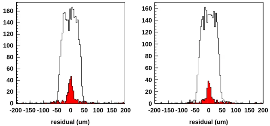
The spatial resolution is obtained as the width of the residual distribution—the distribution of the difference between the extrapolated track position and the centre of cluster.6
Typical residual distributions are shown in Fig.
4. The outline histograms show the result using only single strip clusters: the residuals form a uniform distribution fromp=2 top=2;wherepis the readout pitch, characteristic for binary read- out. The spatial resolution due to single-strip clusters is given by the RMS of a uniform distribution with a width equal to the pitch:
s¼p= ffiffiffiffiffi p12
23mm: The contribution from two- strip clusters is shown in the filled histograms. As the multi-strip clusters predominantly occur in a narrow region in the central region between two strips the resolution of the multi-strip clusters is better than that of single-strip clusters.7Note that the residuals distributions are smeared by the uncertainty on the interpolation of the telescope tracks, approximately 5mm:
interstrip position (pitch) 0 0.1 0.2 0.3 0.4 0.5 0.6 0.7 0.8 0.9 1
efficiency
0 0.2 0.4 0.6 0.8 1
1.0 fC 1.5 fC 2.0 fC 2.5 fC 3.0 fC 4.0 fC
interstrip position (pitch) 0 0.1 0.2 0.3 0.4 0.5 0.6 0.7 0.8 0.9 1
efficiency
0 0.2 0.4 0.6 0.8 1
1.0 fC 1.5 fC 2.0 fC 2.5 fC 3.0 fC 4.0 fC
Fig. 3. Efficiency as a function of the inter-strip position of the incident particle for a non-irradiated (a) and irradiated barrel module (b).
6For endcap modules the residuals are rescaled by the ratio between the barrel pitchð80mmÞand the local pitch to facilitate comparison.
7See the discussion in the next section.
For tracks of normal incidence the fraction of multi-strip clusters is small and the resolution is close to 23mm, independent of the operating parameters. Also, no significant change is observed in the residuals at a threshold of 1 fC after irradiation. The effect of the bias voltage and the incidence angle on charge sharing are discussed in Sections 4.4 and 4.5, respectively.
The residual distribution ofFig. 4is a measure- ment of the spatial resolution of a single detector plane. The stereo angle of 40 mrad between the two detector planes of the SCT module allows the determination of a two-dimensional space point.
The intersection of two 80mm wide strips defines a rhombus with short axisp=cosa=2 and long axis p=sina=2;wherepis the readout pitch andais the stereo angle. The short axis corresponds to theX- axis of the global coordinate system in the test beam, while the long axis is identified with theY- axis. Projecting the uniform distribution in the rhomb on both axes yields the triangular distribu- tions of Fig. 5. A Gaussian fit yields widths of 16mm in X and 850mm in Y. More detailed results on the single module resolution are reported in Ref.[12].
4.3. Median charge
In the binary readout scheme, it is necessary to scan the discriminator threshold through the
charge distribution in order to reconstruct the full signal distribution. The curve of efficiency as a function of threshold, the ‘‘s-curve’’, measures the integrated charge distribution. The collected charge distribution is described by the Landau distribution of the deposited charge convoluted with the Gaussian noise distribution and the effect of charge sharing between neighbouring strips.
The median charge is measured as the charge corresponding to the threshold where 50% effi- ciency is obtained. In practice, the threshold is expressed in equivalent charge and the value for the median charge is obtained directly from a fit with a skewed error function, as in Ref. [13]:
¼maxf x 1þ0:6exxexx exxþexx
(1) wherefdenotes the complementary error function.
The median chargem;the widths;the skewxand the maximum efficiency max are free parameters and x¼ ðqthrmÞ= ffiffiffi
p2
s: This parameterisation describes the data quite accurately.
InFig. 6the ‘‘s-curves’’ of a non-irradiated and an irradiated module are shown for reference operating conditions. Each point corresponds to the efficiency measured on a single run of15,000 events. The lines represent the fit with the function of Eq. (1).
The error on the median charge is dominated by the uncertainties in the calibration. The variation
residual (um)
-200 -150 -100 -50 0 50 100 150 200 0
20 40 60 80 100 120 140 160
residual (um)
-200 -150 -100 -50 0 50 100 150 200 0
20 40 60 80 100 120 140 160
Fig. 4. Single plane residuals with respect to the position interpolated from the beam telescope measurements. The outline histograms correspond to single-strip clusters, the filled histogram to two-strip clusters. Two modules irradiated to 31014protons=cm2: a barrel module (left) and an endcap outer module (right). The discriminator threshold is set to 1 fC. For the endcap module the residuals have been rescaled to the equivalent of a pitch of 80mm:
of the calibration from one chip to the next is evaluated in the beam test by pointing the beam to areas of the detector read out by different chips and measuring the median charge of each chip separately. For non-irradiated modules the chip- to-chip spread in the median charge is of the order of 4%. After irradiation the spread increases to nearly 10% on some modules[28]. Correcting the charge of each chip by measurements of the calibration DAC output improves the uniformity, suggesting that the spread in median charges is due to variations in the components of the calibration circuit[29].
The random error of a single median charge measurement is therefore of the order of 0.1 fC for
non-irradiated modules and 0.3 fC for irradiated modules. In practice, comparison between differ- ent modules is greatly facilitated by the use of the signal-to-noise ratio, the ratio of median charge and the equivalent noise charge.
The average median charge of a significant number of recent unirradiated barrel and outer endcap modules is 3:50:1 fC at a bias voltage of 300 V. Division of the median charge by the equivalent noise charge, which is measured as part of the electrical characterisation of the module, yields a signal-to-noise ratio of 14. For inner endcap modules with shorter, 6 cm strips the lower capacitive load at the amplifier leads to an improved noise performance, yielding a S=N of 20.
A theoretical expectation for the signal height is obtained from a GEANT4 simulation8 of the energy deposition by 180 GeV charged pions in 285mm of silicon. The number of electron–hole pairs created along the track is obtained by dividing the deposited energy by the average energy required to produced an electron hole pair, 3.63 eV [30]. From a detailed simulation of the charge transport and signal induction on the strip the electron contribution to the signal is expected to be small[10,31]. Ignoring the electron contribu- tion, the signal induced on the readout strip is taken to be the sum of the charges of the holes.
single module X residual (cm) -0.01 -0.005 0 0.005 0.01 0
50 100 150 200 250
single module Y residual (cm) -0.2 -0.1 0 0.1 0.2 0
20 40 60 80 100 120
Fig. 5. Residuals of the space point reconstructed on a single, irradiated barrel module with respect to the position interpolated from the beam telescope measurements:X, perpendicular to the long axis of the module (left) andY, parallel to the long axis of the module (right). The discriminator threshold is set to 1 fC.
Threshold (fC)
0 2 4 5
Efficiency
0 0.2 0.4 0.6 0.8 1
1 3 6 7
Fig. 6. Typical efficiency versus threshold ‘‘s-curves’’ for a non- irradiated (solid) and an irradiated (dashed) module under reference conditions (defined in Section 4.1).
8GEANT4 is expected to give a rather accurate prediction for the median deposited energy. For details, see Ref.[10].
Under this assumption the median signal is expected to be 4.0 fC[10,31].
The observed median charge is clearly lower.
Less than 0:1 fC of this difference can be attributed to the measurement procedure, indicating a discrepancy between the deposited and collected charge.
Charge shared between neighbouring strips cannot be re-clustered in the binary readout scheme as it is predominantly below threshold.
The effect of different charge sharing mechanisms on the median collected charge sharing is investi- gated in Ref.[10]. Diffusion of the charge carriers while they drift toward the readout plane can be studied using the position predicted by the telescope. Test beam measurements indicate that the loss of median charge due to diffusion is 0.13–0.16 for all module types. Cross-talk between neighbouring channels is expected to be respon- sible for a charge loss of 6%, i.e.0.26 fC. Finally, the charge carried to neighbouring strips by d- electrons can be quite substantial. However, GEANT4 model calculations show that even though this effect leads to a less pronounced high-energy tail in the charge distribution, the median charge is not significantly affected.
The total charge loss due to the three charge sharing mechanisms is thus expected to amount to 0.4 fC. Thus, charge sharing accounts for most of the discrepancy between the observed median charge, 3.5 fC, and the expected charge deposition, 4.0 fC.
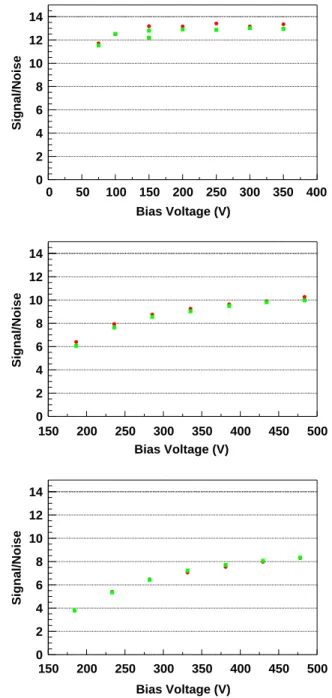
4.4. Detector bias voltage
The bias voltage of the detectors is an important operating parameter. In ATLAS, the maximum voltage is limited by the detector breakdown voltage (greater than 500 V for SCT detectors), the limit of the power supplies (500 V), and the limit imposed by the cooling system. The bias voltage dependence of the performance has there- fore been studied in detail.
Fig. 7 shows the typical dependence of the signal-to-noise ratio on the detector bias voltage for modules before and after irradiation. For non- irradiated modules, of all types, the median signal- to-noise ratio is nearly constant,S=N13, above
Bias Voltage (V)
0 50 100 150 200 250 300 350 400
Signal/Noise
0 2 4 6 8 10 12 14
Bias Voltage (V)
150 200 250 300 350 400 450 500
Signal/Noise
0 2 4 6 8 10 12 14
Bias Voltage (V)
150 200 250 300 350 400 450 500
Signal/Noise
0 2 4 6 8 10 12 14
Fig. 7. Median signal-to-noise ratio versus bias voltage. Top figure: non-irradiated module (all types are similar.) Central figure: irradiated barrel module. Bottom figure: irradiated endcap outer module. In all figures, the round and square markers correspond, respectively, to the readings on the front and back wafers of the module. In cases where the area of the sensor hit by the beam was read out by more than one chip, the results of each chip are indicated separately.
150 V. The charge difference between 150 V and the highest voltage, 300 V, is 0.15 fC. As the bias voltage is decreased towards the depletion voltage (around 75 V in these detectors) the signal gradually decreases. This can be explained as a ballistic deficit of the shaper circuit, i.e. the integration window of the front-end electronics is no longer large compared to the charge collection time of the detector, leading to charge loss. The drift time of the holes becomes comparable to the peaking time of the shaper at a bias voltage of around 100 V. For a detailed discussion of charge collection times, see Refs.[32,33].
The relation between signal and bias voltage for irradiated modules is more complicated. The actual bias voltage on the silicon is lower than the supplied voltage by up to 30 V due to the voltage drop in the hybrid bias resistor, in turn due to the much higher, and strongly temperature dependent, leakage current. The horizontal axes in Fig. 7 have been corrected for this effect. After irradiation the depletion voltage has significantly increased, estimated to be around 250 V for these detectors. Above the depletion voltage the col- lected charge continues to rise slowly. The signal collected at a bias voltage of 350 V is approxi- mately 90% of that at the maximum bias voltage of nearly 500 V.
Due to the increased noise, the signal-to-noise ratio of irradiated modules does not reach the pre- irradiation value, even at the highest available bias voltage. Barrel and endcap modules irradiated to 1:61014protons=cm2; around half the reference fluence, have a median signal-to-noise ratio of 110:5 at 500 V. For modules irradiated to the maximum fluence, 31014protons=cm2;the mea- surements are scattered between values 7 and 11.
The large spread between modules is not com- pletely understood but may partly be due to dose uncertainty. The endcap modules tend to have signal-to-noise ratios that are in the lower part of the distribution, but the limited statistics does not exclude systematic effects due to ABCD batch variations.
Various explanations exist for the high over- depletion needed to approach full charge collec- tion. Measurements by the ROSE collaboration [34]indicate that there is considerable charge loss
due to trapping of the charge carriers in radiation- induced lattice defects. Assuming a constant trapping probability per unit time, the effect is bias voltage dependent through the charge collec- tion time. For small over-depletion, the different field distribution across the silicon in type-inverted bulk material may lead to a ballistic deficit of the shaper.
In irradiated, type-inverted pþn detectors the junction forms at the backplane, between the nþ material of the backplane and the p-bulk. Thus, if the bias voltage is lower than the depletion voltage the depleted region does not reach the readout side of the detector. A small signal is nevertheless induced on the strips across the dead region.
4.5. Incidence angle and magnetic field
In ATLAS the SCT modules will be situated within a 2 T magnetic field. Also, tracks will not generally be perpendicularly incident on the detector plane. Therefore, an important subject of study is the influence of the magnetic field and incidence angle on the performance of the modules.
In the August 2001 beam test [12] threshold scans were performed at various angles, both without magnetic field and in the 1.56 T field of the Morpurgo magnet. In this section the dependence of the most important parameters—efficiency at the operation threshold, median collected charge and spatial resolution—on the incidence angle and field is discussed.
Two orthogonal orientations have been studied.
First, the simpler case is considered where the projection of the particle trajectory on the read- out plane is parallel to the strips,9the longer path length through the silicon leads to an increase of the median charge with 1=cosðaÞ:This behaviour has been confirmed in beam tests up to angles of 16 in 2001[12]and in a second measurement at 35in 2002[28](see the leftmost figure ofFig. 8).
9In the SCT this angle is determined by the detector geometry. The angle reaches quite large values (up to 70o) for the most forward modules on the barrel and for the disk closest to the interaction point.
In the second orientation the projection of the particle trajectory is perpendicular to the strips.
For a particle from the ATLAS interaction point non-perpendicular incidence arises from the de- flection of particles in the solenoidal magnetic field, the tilt of the module, and the range of angles which the module subtends. The incidence angle in this orientation is generally smaller: the tilt angle of the barrel modules is10;of the same order as the deflection angle of a 1 GeV particle.
The longer path length again leads to a small increase of the signal. But, in this orientation the projection of the particle trajectory on the readout plane is perpendicular to the readout strips. For large incidence angles the projected distance becomes significant compared to the pitch and charge sharing between neighbouring strips be- comes important. The net effect is a decrease of the median collected charge on a single strip as shown at right inFig. 8.
In a strong magnetic field the Lorentz force deviates the drifting carriers.Fig. 9shows how the Lorentz force is equivalent to a rotation by a small angle YL¼mHB¼rHmB; where mH the Hall mobility, the conduction mobilitym multiplied by the Hall scattering factorrH:In pþn type sensors, the signal is predominantly due to holes and the Lorentz angle is of the order of a few degrees.
In August 2001 the combined effect of incidence angle and magnetic field was studied in an
orientation representative for barrel modules at Z¼0: The modules were biased to nominal bias voltages: 150 V for non-irradiated modules, and 350 V after the full expected dose. The modules are naturally classified in two groups: irradiated and non-irradiated modules. The results are presented as averages over all (non-) irradiated barrel modules, the errors representing the variation between different modules.
A sensitive measure of charge sharing is the average cluster size. Here, the cluster size depen- dence on angle in a magnetic field is used to determine the Lorentz angle. Noise clusters are degrees
5 10 15 20 25 30 35 40
Q/Q(0)
1 1.05 1.1 1.15 1.2
2002 test beam B053
2001 test beam B029
degrees
-20 -10 0 10 20 30 40
Median Charge (fC)
1.5 2 2.5 3
3.5 2001 test beam
B018
2002 test beam KB-105
Fig. 8. Leftmost figure: median charge versus incidence angle in theR–zorientation. The points are normalised with respect to the 0 result. The continuous line is the function 1=cosacorresponding to the simple geometric behaviour expected from the increased path length. Rightmost figure: median charge versus incidence angle in theR–fplane. The continuous line corresponds to a fit with a parabola. In both figures, the 35point is a result from the 2002 test beam, while the other measurements refer to a barrel module measured in 2001. The detector bias voltage is 150 V.
+ + + + ++
++ + + + +
+ + ++
+ + +
+ +
+ +
P+
n+ B
Beam Beam
α ΘL
Fig. 9. Representation of the effect of the incidence angle and the application of a magnetic field. The angleais the incidence angle of the beam particle, yL is the Lorentz angle of the drifting carriers.
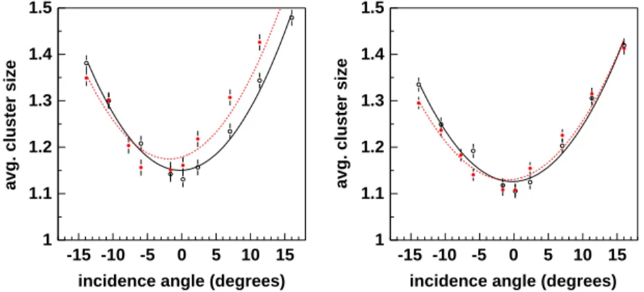
excluded by placing a 200mm window around the track position predicted by the telescope. Fig. 10 shows the average cluster size as a function of incidence angle (filled markers). The open markers show the same measurement in a 1.56 T magnetic field.
The increase of cluster size at non-perpendicular incidence reflects the increased charge sharing. The effect of the magnetic field is a shift of the distribution by the Lorentz angle.
The value of the Lorentz angle is determined as the minimum of the cluster size versus angle curve.
The measurements from all modules in both groups have been combined. The statistical error is taken to be the standard deviation of the measurements of a group. As a cross check, the fit results for data taken without magnetic field have been calculated. The result Y0¼0:40:2 reflects the overall uncertainty in the angle scale.
The Lorentz angle obtained for both groups, non- irradiated and irradiated modules, is then:
YLð150 V;non-irradiatedÞ ¼3:30:3 (2) YLð350 V;irradiatedÞ ¼2:10:4: (3) As the irradiated modules are biased at a higher voltage, the observed difference could be due to an electric field dependence of the Lorentz angle or a change in the properties of the charge carriers due to irradiation. In the literature, the effect of proton
irradiation on the mobility and thus Lorentz angle of holes is found to be compatible with no effect [32,35,36]. The difference in voltage, i.e. the electric field inside the detector, has an effect on YL through the electric field dependence of the carrier mobilitym[35,37–39]. Applying the theore- tical model of Ref. [39] to beam test conditions (silicon temperature T ¼261 K; thickness d ¼ 285mm and field B¼1:56 T) a prediction of YLð150 VÞ ¼3:3 and YLð350 VÞ ¼2:4 is ob- tained. The predictions agree within errors with our measurements.
In the range of angles ½14;16 studied in the beam test no significant effect on the efficiency is observed at a threshold of 1 fC. For irradiated modules a small effect becomes visible when the discriminator threshold is raised to 1.2 fC. Still, the efficiency is over 97% for all angles.
As discussed in Section 4.2 the spatial resolution with binary readout depends on the number of strips in the cluster. An increase in the number of multi-strip clusters is expected to lead to a better resolution. In Fig. 11 the effect of the incidence angle on the spatial resolution of non-irradiated (leftmost figure) and irradiated modules (right- most figure) is shown. The difference between the worst (0) and the bestð15Þresolution is around 2mm:Again the magnetic field causes a shift by the Lorentz angle.
incidence angle (degrees) -15 -10 -5 0 10 15
avg. cluster size
1 1.1 1.2 1.3 1.4 1.5
incidence angle (degrees) -15 -10 -5 0 10 15
avg. cluster size
1 1.1 1.2 1.3 1.4 1.5
5 5
Fig. 10. Cluster size versus angle for non-irradiated modules at 1 fC (left) and irradiated at 1 fC (right). The filled markers represent measurements with a magnetic field of 1.56 T, the open markers correspond to the same measurement without field. Both sets of measurements have been fit with a parabola (continuous line for the data with magnetic field, dashed line without field) to guide the eye.