The Barrel Modules of the ATLAS SemiConductor Tracker
A. Abdesselam22, T. Akimoto31, P.P. Allport15, J. Alonso14, B. Anderson32, L. Andricek18, F. Anghinolfi5, R.J. Apsimon27, G. Barbier9, A.J. Barr4,32, L.E. Batchelor27, R.L. Bates10,
J.R. Batley4, G.A. Beck26, P.J. Bell5,16, A. Belymam26, J. Bernabeu34, S. Bethke18, J.P. Bizzell27, J. Bohm24, R. Brenner33, T.J. Brodbeck13, Z. Broklova23, J. Broz23, P. Bruckman De Renstrom6,22, C.M. Buttar10, J.M. Butterworth32, C. Carpentieri8, A.A. Carter26, J.R. Carter4*, D.G. Charlton3, A. Cheplakov10, E. Chesi5, A Chilingarov13,
S. Chouridou28, M.L. Chu30, V. Cindro11, A. Ciocio14, J.V. Civera34, A. Clark9, P. Coe22, A-P. Colijn19, T. Cornelissen19, D.P. Cosgrove28, M.J. Costa5, W. Dabrowski7, J. Dalmau26, K.M. Danielsen21, I. Dawson29, B. Demirkoz22, P. Dervan29,15, Z. Dolezal23,
M. Donega9,5, M. D’Onofrio9, O. Dorholt21, J.D. Dowell3, Z. Drasal23, I.P. Duerdoth16, M. Dwuznik7, S. Eckert8, T. Ekelof33, L. Eklund33, C. Escobar34, V. Fadeyev14, L. Feld8,
P. Ferrari5, D. Ferrere9, L. Fiorini4, R. Fortin5, J.M. Foster16, H. Fox8, T.J. Fraser32, J. Freestone16, R. French29, J. Fuster34, S. Gadomski6, B.J. Gallop3,27, C. García34,
J.E. Garcia-Navarro34, M.D. Gibson27, S. Gibson22, M.G.D. Gilchriese14, J. Godlewski5,6, S. Gonzalez-Sevilla34, M.J. Goodrick4, A. Gorisek5, E. Gornicki6, A. Greenall15, C. Grigson29, A.A. Grillo28, J. Grosse-Knetter5, C. Haber14, K. Hara31, F.G. Hartjes19, D. Hauff18, B.M. Hawes22, S.J. Haywood27, N.P. Hessey19, A. Hicheur27, J.C. Hill4, T.I. Hollins3, R. Holt27, D.F. Howell22, G. Hughes13, T. Huse21, M. Ibbotson16,
Y. Ikegami12, C. Issever22, J.N. Jackson15, K. Jakobs8, P. Jarron5, L.G. Johansen2, T.J. Jones15, T.W. Jones32, P. de Jong19, D. Joos8, P. Jovanovic3, S. Kachiguine28, J. Kaplon5, Y. Kato31, C. Ketterer8, H. Kobayashi31, P. Kodys23, E. Koffeman19, Z. Kohout25, T. Kohriki12, T. Kondo12, S. Koperny7, G. Kramberger11, P. Kubik23,
J. Kudlaty18, T. Kuwano31, C. Lacasta34, D. LaMarra9, J.B. Lane32, S.-C. Lee30, C.G. Lester4, M. Limper19, S. Lindsay17,15, M.C. Llatas9, F.K. Loebinger16, M. Lozano1, I. Ludwig8, J. Ludwig8, G. Lutz18, J. Lys14, M. Maassen8, D. Macina9,5, A. Macpherson5,
C. MacWaters27, S.J. McMahon27, T.J. McMahon3, C.A. Magrath19, P. Malecki6, I. Mandić11, M. Mangin-Brinet9, S. Martí-García34, G.F.M. Martinez-Mckinney28,
J.M.C. Matheson27, R.M. Matson27, J. Meinhardt8, B. Mikulec9, M. Mikuž11, M. Minagawa31, J. Mistry26, V. Mitsou34, P. Modesto34, S. Moëd9, B. Mohn2, G. Moorhead17, J. Morin26, J. Morris26, M. Morrissey27, H-G. Moser18, A.J.M. Muijs19,
W.J. Murray27, K. Nagai26, K. Nakamura31, Y. Nakamura31, I. Nakano20, A. Nichols27, R. Nicholson29, R.B Nickerson22, R. Nisius18, V. O'Shea10, O.K. Oye2, M.J. Palmer4, M.A. Parker4, U. Parzefall8, J.R. Pater16, S.J.M. Peeters19, G. Pellegrini1,
H. Pernegger5, E. Perrin9, A. Phillips4, P.W. Phillips27, K. Poltorak7, S. Pospisil25, M. Postranecky32, T. Pritchard5, J.M. Rafi1, P.N. Ratoff13, P. Reznicek23, R.H. Richter18,
D. Robinson4, S. Roe5, F. Rosenbaum28, A. Rudge5, K. Runge8, H.F.W. Sadrozinski28, H. Sandaker21, D.H. Saxon10, J. Schieck18, K. Sedlak22, A. Seiden28, H. Sengoku31,
*Corresponding author. Tel.: +44-1223-337235; fax: +44-1223-353920; e-mail:jrc1@hep.phy.cam.ac.uk (J.R. Carter)
A. Sfyrla9, S. Shimma31, K.M. Smith10, N.A. Smith15, S.W. Snow16, M. Solar25, A. Solberg2, B. Sopko25, L. Sospedra34, E. Spencer28, E. Stanecka6,5, S. Stapnes21,
J. Stastny24, M. Stodulski6, B. Stugu2, R. Szczygiel6, R. Tanaka20, G. Tappern27, G. Taylor17, P.K. Teng30, S. Terada12, R.J. Thompson16, M. Titov8, B. Toczek7, D.R. Tovey29, A. Tricoli22, M. Turala6, P.R. Turner15, M. Tyndel27, M. Ullán1, Y. Unno12,
E. Van der Kraaij19, I. van Vulpen19, G. Viehhauser22, E.G. Villani27, V. Vorobel23, M. Vos34, R. Wallny5, M.R.M. Warren32, R.L. Wastie22, M. Weber27, A.R. Weidberg22,
P. Weilhammer5, P.S. Wells5, M. Wilder28, I. Wilhelm23, J.A. Wilson3, M. Wolter6.
1Centro Nacional de Microelectrónica CNM-IMB (CSIC), Barcelona, Spain.
2Department of Physics and Technology, University of Bergen, N 5007 Bergen, Norway.
3School of Physics and Astronomy, University of Birmingham, Birmingham B15 2TT, UK.
4Cavendish Laboratory,University of Cambridge, J.J. Thomson Avenue, Cambridge, CB3 0HE, UK.
5European Laboratory for Particle Physics (CERN), 1211 Geneva 23, Switzerland.
6Institute of Nuclear Physics PAN, Cracow, Poland.
7Faculty of Physics and Applied Computer Science, AGH University of Science and Technology, Cracow, Poland.
8Fakultät für Physik, Albert-Ludwigs-Universität, Freiburg, Germany.
9DPNC, University of Geneva, CH 1211 Geneva 4, Switzerland.
10Department of Physics and Astronomy, University of Glasgow, Glasgow, UK.
11Jožef Stefan Institute and Department of Physics, University of Ljubljana, Ljubljana,Slovenia.
12KEK, High Energy Accelerator Research Organisation, Oho 1-1, Tsukuba, Ibaraki 305-0801, Japan.
13Department of Physics and Astronomy, University of Lancaster, Lancaster, UK.
14Lawrence Berkeley National Laboratory, Berkeley, California, USA.
15Oliver Lodge Laboratory, University of Liverpool, Liverpool, UK.
16The School of Physics and Astronomy, University of Manchester, Manchester M13 9PL, UK.
17University of Melbourne, Parkville, Victoria 3052, Australia.
18Max-Planck-Institut fűr Physik (Werner-Heisenberg-Institut), Főhringer Ring 6, D-80805 Műnchen, Germany.
19NIKHEF, Amsterdam, The Netherlands.
20Okayama University, The Graduate School of Natural Science and Technology, Tsushima-naka 3-1-1, Okayama 700-8530, Japan.
21Department of Physics, P.O. Box 1048 Blindern, N-0316 Oslo, Norway.
22Physics Department, University of Oxford, Keble Road, Oxford OX1 3RH, UK.
23Charles University in Prague, Faculty of Mathematics and Physics, V Holesovickach 2, CZ 18000 Prague, Czech Republic.
24Institute of Physics of the Academy of Sciences of the Czech Republic, Na Slovance 2, CZ 18221 Prague 8, Czech Republic.
25Czech Technical University in Prague, Zikova 4, CZ 16636 Prague 6, Czech Republic.
26Department of Physics, Queen Mary University of London,, Mile End Road,London E1 4NS, UK.
27Rutherford Appleton Laboratory, Chilton, Didcot, Oxfordshire OX11 OQX, UK.
28Santa Cruz Institute for Particle Physics, University of California, Santa Cruz, California, USA.
29Department of Physics and Astronomy, University of Sheffield, Sheffield, UK.
30Institute of Physics, Academia Sinica, Taipei, Taiwan.
31University of Tsukuba, Institute of Pure and Applied Sciences, 1-1-1 Tennodai, Tsukuba, Ibaraki 305-8571, Japan.
32Department of Physics and Astronomy, University College London, Gower Street, London WC1E 6BT, UK.
33Uppsala University, Department of Nuclear and Particle Physics, P.O. Box 535, SE-75121 Uppsala, Sweden.
34Instituto de Física Corpuscular (IFIC), Universidad de Valencia-CSIC, Valencia, Spain.
Abstract
This paper describes the silicon microstrip modules in the barrel section of the SemiConductor Tracker (SCT) of the ATLAS experiment at the CERN Large Hadron Collider (LHC). The module requirements, components and assembly techniques are given, as well as first results of the module performance on the fully-assembled barrels that make up the detector being installed in the ATLAS experiment.
PACS: 29.40
Keywords: ATLAS; SCT; silicon; microstrip; barrel; module; LHC
1. Introduction
The ATLAS experiment [1] is being constructed to explore the physics of 14 TeV proton-proton collisions at the CERN Large Hadron Collider (LHC) [2], with first beam expected in 2007. The ATLAS Inner Detector (ID) [3] tracks charged particles coming from the interaction region, and consists of a pixel detector (Pixel), surrounded by the SemiConductor Tracker (SCT), which is itself surrounded by a gaseous/polypropylene foil transition radiation tracker (TRT). The overall ID is 2.3 m in diameter and 7 m in length. For analyzing the momenta of charged particles, a 2 Tesla uniform magnetic field is provided by a superconducting central solenoid [4] which is integrated inside the cryostat of a liquid argon electromagnetic calorimeter. A quadrant view of the ID together with the solenoid is shown in Fig. 1. Because of the high energy of the proton-proton collisions, large numbers of particles are generated in one interaction, and multiple interactions are expected in one crossing of the proton bunches. The main requirements for the ID are precision tracking of charged particles in the environment of numerous tracks, capability of bunch-crossing identification, tolerance to large radiation doses, construction with the least possible material, and a capability for electron identification within the ID.
The ID consists of barrel and endcap regions in order to minimize the material traversed by particles coming from the interaction region at its centre. The barrel region is made of co-axial cylindrical layers and the endcap of disk layers. The Pixel and SCT detectors use silicon semiconductor technology for precision measurement.
In the barrel region there are three Pixel and four SCT layers, each of which is able to read out a position in two dimensions. This paper describes the SCT detector modules of the barrel region. The SCT endcap modules are described elsewhere [5].
SOLENOID COIL
TRT TRT
SCT (Barrel) SCT (Endcap)
PIXEL
PPB1
PPF1 CRYOSTAT
CRYOSTAT
PIXEL SUPPORT TUBE
BEAM PIPE
eta=1.0 eta=1.5
746847.5 934
1084 1262 1377
1747 2072 2462 2727
R299 R371 R443 R514
R50.5 R88.5 R122.5
R230 R559
R1080 R1150
401 495
580 650
R150 R89
R560
R270
R338
R408 R439
R36 eta=2.0
eta=2.5 Y
(R)
Z 715
0 0
RADIUS R635
R999 839 2713
Fig. 1 A quadrant view of the inner detector (ID) together with the central solenoid inside the cryostat of the liquid argon electromagnetic calorimeter.
2. Design specifications
2.1. Overview of SCT Barrel Module Requirements
The four SCT cylinders in the barrel region (termed Barrels 3, 4, 5 and 6) have radii between 299 mm and 514 mm and a full length of 1492 mm. Their surface areas are tiled with segmented detector elements, the SCT barrel modules, to provide complete four-layer digitization coverage for particles coming from a length of ± 76 mm about the nominal interaction point on the central axis. This is the expected ± 2 sigma length of the beam interaction point. The barrel cylinder parameters and the numbers of modules are summarized in Table 1. The design adopted for the barrel module, illustrated in Fig. 2, is to use four near-square silicon microstrip sensors, two on the top and two on the bottom side, with the readout hybrid placed near the centre of the unit. The design has minimum structure near the end edges to allow overlap of the sensitive regions of adjacent modules on a barrel. A core sheet, known as the module baseboard, provides the thermal and mechanical structure. It is sandwiched between the top and the bottom sensors, and extends sideways to include the beryllia facing regions shown in Fig. 2. The hybrid assembly bridges over the sensors and is held clear of their surfaces by feet that are glued to the beryllia facings. The module is attached to the support structure at three points, two in the large (cooling side) and one in the small (far side) facing regions. The large facing contacts a cooling element that runs along the length of the modules on a barrel.
The required tracking precision is obtained using silicon microstrip sensors with a readout pitch of 80 µm and a binary (on-off) readout scheme. The back-to-back sensor pair in a module has a stereo rotation angle of 40 mrad. A module is mounted on a barrel with its strips on one side parallel to the barrel axis (z), resulting in a precision of 17 µm in the r-phi coordinate and 580 µm in the z coordinate from the correlation obtained through fitting. The mechanical tolerance for positioning sensors within the back-to-back pair must be better than 8 µm transverse to the strip direction.
The high accumulated radiation levels at the LHC have severe consequences for silicon sensors, causing increased leakage current and type inversion, and give rise to the need to operate the sensors at about –7 oC.
The maximum expected integrated fluence after 10 years of operation in the SCT is ~2x10¹⁴ 1 MeV-neutron-equivalent/cm2 (at the upper limit of uncertainty of 50% coming from the total cross section and particle multiplicity). The corresponding sensor bias voltage required for high charge collection efficiency will be in the range 350-450 V, depending upon SCT warm-up scenarios. This will result in a total leakage current of ~ 0.5 mA for an individual sensor operated at –7 oC at a bias voltage of 450 V. The leakage current is strongly dependent on temperature, roughly doubling every 7 oC. The heat generation is therefore a strong function of the temperature of the sensors in the module. The power consumption of the front-end ASICs is expected to be
~5.5 W nominal and ~7.5 W maximum per module. These values are larger than originally anticipated [3], and have been amongst the driving factors in a significant evolution of the overall SCT design, and in particular that of its cooling system.
Thermal considerations, and especially the danger of thermal run-away, lead to a module design where the effective in-plane thermal conductivity must be increased beyond that of silicon. This is achieved by the use of high thermal conductivity material in the baseboard, which is laminated as part of the detector sandwich. The SCT will undergo temperature cycling over the range -20 oC to +25 oC in a controlled sequence, and it must survive, in the event of cooling or local power fluctuations, up to temperatures approaching 100 oC. This requires the module to have a small coefficient of thermal expansion and to be capable of limited elastic deformation, as the precision of the tracking measurement depends on the return to a stable profile after changes in operating conditions. The SCT modules are in the tracking volume and are therefore required to have minimal mass.
Table 1: SCT barrel cylinder parameters and the number of modules
Barrel cylinder Radius (mm) Length (full) (mm) Tilt angle in phi (deg) Number of modules
Barrel 3 299 1492 11 384
Barrel 4 371 1492 11 480
Barrel 5 443 1492 11.25 576
Barrel 6 514 1492 11.25 672
Total 2112
Note: Tilt angle is the angle of the modules relative to the local tangent to the surface of their supporting cylinder.
Fig. 2: A 3D-view of the ATLAS SCT barrel module. The overall length of the module is 128 mm.
2.2. Specifications of the components to provide the necessary module performance
2.2.1. Silicon microstrip sensors
Full details of the SCT barrel silicon microstrip sensors are given elsewhere [6,7]. Their final specification was reached after several years of R&D. The principal requirements were to match the parameters of the chosen binary readout electronics [8] (section 2.2.3), to accommodate the high levels of radiation within ATLAS, to maximize the sensitive area of the sensor, to minimize material and to provide modules with very high tracking efficiency and low noise occupancy, both before and after irradiation. The design was also required to be simple, using single-sided processing, for economic reasons. The choice was p-in-n microstrip sensors. All 10,650 SCT barrel sensors were provided by Hamamatsu Photonics [9] and made from standard high resistivity 4-inch silicon wafers. The sensors are identical throughout the barrel SCT, with a rectangular geometry and 768 AC-coupled readout strips at a pitch of 80 µm. Table 2 summarizes their principal parameters, pre- and post-irradiation. The sensors are to be operated at about 150 V bias voltage initially. After 10 years of LHC operation, those in the innermost regions are expected to be operated at about 450 V bias voltage, with over 90%
charge collection efficiency.
A corner detail of a sensor is shown in Fig. 3, where the polysilicon bias resistors, the bond pad layout and the edge bias and guard structures are visible. Some of the fiducial marks used for the mechanical alignment of sensors during module assembly (section 3.2.1) are also shown. Apart from pads used for bonding and probing, the front sides of the sensors are fully passivated. The passivation, together with stringent requirements on the quality of the cut edge (the latter being at the backplane bias voltage), are important to reduce the risk of creating accidental high voltage shorts during module construction or operation.
During pre-series production, both <111> and <100> orientations for the silicon substrate were evaluated, and found to be equally good for use in the SCT. The series production was with <111> silicon, for reasons of availability of supply. Pre-series sensors were used to make 61 (2.6%) of the SCT barrel modules. Passivation in the edge region was increased between the pre-series and main series sensor production.
Table 2: The major parameters of the SCT barrel silicon microstrip sensors
Parameter Value and description
Length 63960 ± 25 μm finish (64 mm nominal centre cutting line to cutting line) Width 63560 ± 25 μm finish (63.6 mm nominal centre cutting line to cutting line) Edge Quality No edge chip or crack to extend inwards by > 50 µm
Thickness 285 ± 15 μm
Uniformity of thickness within a sensor 10 μm
Flatness Flat when unstressed to within 200 μm
Wafer n-type, >4 kΩ high resistivity silicon, <111> or <100> orientation Implanted strips 768 + 2 strips, p-implant, < 200 KΩ/cm
Read-out strips 768 strips, aluminium, < 15Ω/cm, capacitively coupled with implant strips
Strip pitch 80μm
Implant strip width 16 µm
Read-out strip width 22 μm
Bias resistors Polysilicon, 1.25 ± 0.75 MΩ
Rinter-strip >2×RBIAS at operating voltage after correcting for bias connection
Interstrip Capacitance (pre-irradiation) Nearest neighbour on both sides, < 1.1 pF/cm at 150 V bias measured at 100 kHz Interstrip Capacitance (post-irradiation) Nearest neighbour on both sides < 1.5 pF/cm at 350 V bias, measured at 100 kHz
Ccoupling ≥ 20 pF/cm, measured at 1 kHz.
Reach-through protection 5 to 10 μm gap from end of implanted strip to grounded implant Sensitive region to cut edge distance 1mm
High Voltage Contact Large metalised contactable n-layer on back.
Read-out pad 200 × 56 μm bond pads, ≥ two rows, daisy-chainable Passivation Passivated on the strip side and un-passivated on the backplane Identification Every 10th strip, starting at 1 for the first read out strip
Maximum operating voltage 500 V
Total Leakage Current (pre-irradiation) < 20 μA at 15 oC up to 350 V bias voltage
Total Leakage Current (post-irradiation) < 250 μA at –18 oC up to 450 V bias voltage (on the sensor) Microdischarge (pre-irradiation) None below 350 V bias
Microdischarge (post-irradiation) < 5% increase in the noise of any channel with bias increase from 300 V to 400 V Bad strips (pre-irradiation) A mean of ≥ 99% good readout strips per sensor, with all sensors having > 98% good strips Bad strips (post-irradiation) Number of bad strips at 350 V bias satisfying the above pre-irradiation bad strip specification
Fig. 3: Photograph of a corner of an SCT barrel silicon microstrip sensor, showing the guard structure, a selection of fiducial alignment marks, the bias ring, polysilicon resistors, and the metallization above implant strips, including wire-bonding pads.
2.2.2. Baseboards
The baseboard is the central element of the module, providing its thermal management, mechanical integrity and precision attachment to the barrel. Within the module the baseboard is sandwiched between the two planes of silicon sensors. To minimize the overall material within a module, the baseboard is designed to have the least possible mass compatible with both the mechanical requirements, and with providing the necessary internal heat transfer and the interface to the external heat sink. The thermal load comes from the 12 ASICs and, after irradiation, the silicon sensors (sections 2.1 and 2.3.2).
The requirements are well met by the customized thermal-mechanical baseboard shown in Fig. 4(a) and Fig.
4(b), developed specifically for this project using new processes [10]. These include directly encapsulating 380 µm thick anisotropic thermal pyrolytic graphite sheets [11] with epoxy, and at the same time interfacing 250 µm thick beryllia facing plates [12] into the structure. The highly ordered graphite crystal plane is parallel to the baseboard surface, providing the high thermal conductivity path for the heat flow, and the intrinsic fragility of such graphite plates is circumvented by the encapsulation process. The result is a baseboard with the necessary robustness, mechanical integrity and external electrical insulation, and one that is easily handled in the module construction process. The production of some 3,000 baseboards for the ATLAS SCT project was carried out at CERN by a collaboration of ATLAS members [13]. Details of the baseboard fabrication and processing are given in [14].
The larger of the two pairs of beryllia facing plates within each baseboard have holes that are aligned with similar holes in the graphite substrate to provide through-holes for attaching modules to the cylinders that support them within ATLAS. The precision alignment in the overall SCT structure comes from aluminium washers that are attached with epoxy to the upper beryllia facing plate of the baseboard. The washers are positioned above the through-holes using jigs that set the relative separation of their centres and also the orientation of their line of centres [14]. One washer has a circular hole of diameter 1.800 mm, tolerance (−0.005, + 0.010) mm, which determines a precise spatial location for the module, and the second washer maintains similar precision in the direction perpendicular to the module sensor strips while its opening is slotted in the other direction to provide for mechanical tolerances in assembly. These washers can be seen in Fig. 4(a). Module attachment to the cylinder within ATLAS is completed through a clamped third mounting point at the edge of the small beryllia facing.
Electrical high voltage bias contact to the back surface of the attached silicon wafers is through areas where the encapsulation is removed from the baseboard surfaces during production, and electrically conducting epoxy is applied during the wafer attachment process (section 3.2.1). The bias connectivity is completed using the electrical conductivity of the graphite core, via small holes, filled with electrically conducting epoxy [14], in the small and large facings within the upper surface of the baseboard (see Fig. 4(a)). The holes in the beryllia facings have gold-plated surround pads that subsequently allow connection to be made with wire-bonds to the bias potential supplied from the module hybrid (section 3.2.4). These features can be seen in the picture of the upper side of a baseboard in Fig. 4(a), while beryllia facings without bias contacts or washers are shown on the lower-side of the baseboard in Fig. 4(b), and are inclined by 40 mrad with respect to those on the upper surface for purposes of silicon sensor mounting (section 2.3.1).
When assembled in the SCT, the conducted heat leaves the module via the larger beryllia facing on the baseboard lower surface, which is interfaced to an aluminium block via a layer of thermal grease, approximately 100 µm thick, and a copper-kapton shunt-shield. The block itself is soldered to a cooling pipe in which the heat is used as latent heat to evaporate liquid C3F8 at temperatures close to −25 0C.
The baseboard properties are summarized in Table 3.
Table 3: Specifications of the SCT barrel baseboard
Parameters Central Value Tolerance Limit
Thermal pyrolytic graphite substrate:
(i) in-plane thermal conductivity (ii) transverse thermal conductivity
1650 W/m K at 20 °C
~6 W/m K
>1450 W/m K at 20 °C
Encapsulated baseboard thickness in sensor area 430 µm ± 50 µm Baseboard thickness in beryllia facing area 930 µm ± 70 µm Beryllia facing thermal conductivity ~280 W/m K at 20°C
Fig. 4: (a) Baseboard Upper surface (b) Baseboard Lower Surface
2.2.3. ASICs
The ABCD3TA chip provides all functions required for processing the signals from 128 strips of a silicon strip detector in the ATLAS experiment. It is a single chip implementation of a binary readout, using DMILL technology. The main functional blocks are front-end, input register, pipeline, de-randomizing buffer, command decoder, readout logic, and threshold and calibration control sections. The die size of the ABCD3TA chip is 6550 μm x 8400 μm. The full details of the ASIC are described elsewhere [8].
The main requirements of the chip are summarized in Table 4 and the pad layout is shown in Fig. 5. The front-end section performs charge integration, pulse shaping and amplitude discrimination. The threshold value for the amplitude discrimination is provided as a differential voltage from an internal programmable DAC. The outputs of the discriminators are latched either in the edge-sensing mode or in the level-sensing mode. At the start of each clock cycle the chip samples the outputs from the discriminators and stores these values in a pipeline until a decision can be made on whether to keep the data. Upon receipt of a Level 1 Trigger signal the corresponding set of values, together with their neighbours in time, are copied into the readout buffer serving as a de-randomizing buffer. The data written into the readout buffer are compressed before being transmitted off the chip. Transmission of data from the chip is by means of token passing. The chip incorporates features that, with the hybrid circuit, enable the system to continue operating in the event of a single chip failure. It is a system requirement that less than 1% of data will be lost due to the readout buffer on the chip being full, provided that the average occupancy of the silicon strip detectors is below 2% at an average trigger rate of 100 kHz. This is to be compared with the expected worst case strip occupancy averaged over strips and time, which is only 1%.
The ABCD3TA design provides uniformity of thresholds, a critical parameter for the binary architecture, by implementation of an individual threshold correction in every channel using a 4-bit digital-to-analogue converter (TrimDAC) per channel. The TrimDAC has four selectable ranges to cope with the spread of threshold offsets, which increases by a factor of three after a fluence of 3 × 10¹⁴ protons/cm2.
Each channel has an internal Calibration Capacitor connected to its input for purposes of simulating a hit strip.
The Calibration Capacitors are charged by an internal chopper circuit that is triggered by a command. Every fourth channel can be tested simultaneously, with group selection determined by two binary coded Calibration Address inputs. The voltage step applied to the Calibration Capacitors by the chopper is determined by an internal DAC. A tuneable delay of the calibration strobe with respect to the clock phase covers approximately two clock periods.
Table 4: Requirements of the ABCD3TA chip
Parameter Description Signal polarity Positive signals from p-type strips
Input protection voltage step of 450 V of either polarity with a cumulative charge of 5 nC in 25 ns Gain at the discriminator input 50 mV/fC
Peaking time 20 ns
Noise (ENC) on fully populated modules Typically 1500 electrons rms for an unirradiated module Typically 1800 electrons rms for an irradiated module Noise occupancy at 1fC threshold < 5x10⁻⁴
Threshold setting range 0 fC to 12.8 fC with 0.05 fC step
Timewalk 16 ns (1.25 fC to 10 fC with 1fC threshold)
Double Pulse Resolution 50 ns for a 3.5 fC signal followed by a 3.5 fC signal Power consumption (of fully populated module) < 6 W nominal
8400
6550
131 input pads: 43x120 pitch in rows: 96 row separation: 80
VDDDGND
tokenout0Btokenout0datain0Bdatain0clk0Bclk0
clk1 clk1B
id<4>id<3>id<2>id<1>id<0>mastercom1Bcom1com0Bcom0selectresetBledBleddataout0dataout0Btokenin0tokenin0BDGNDDGND
VDD
VDD
VDD DGND ring_a
GNDA VCC
tokenoutBPB tokenoutBP datainBPB datainBP tokeninBPB
tokeninBP dataoutBPB dataoutBP
pads: 120 x 180 pitch: 330
spare pads for testing only pads: 120 x 180
pitch: 330
pads: 200 x 180pitch: 270
pads: 120 x 180pitch: 180
pads: 160 x 180pitch: 200
pads: 120 x 180pitch: 180
pads: 160 x 180pitch: 200
pads: 120 x 180pitch: 180
pads: 200 x 140 pitch: 300
to be bonded to analog gnd
VTHN VTHP
IP_PR IS_PR
ABCD3TA
D_ISH detgnd
external decoupling of ISH line
pads: 100 x 140 pitch: 200
ring_a GNDA VCC VTHN VTHP
cal1 cal2 cal0 detgnd
cal3
to be bonded to analog gnd
pads: 100 x 140 pitch: 200 pads: 200 x 140 pitch: 300
detgnd detgnd
Fig. 5: The pad layout of the ABCD3TA chip.
2.2.4. Hybrids
The SCT barrel hybrid carries electrical circuitry and 12 ABCD3TA readout chips, 6 on the top side (termed link0) and 6 on the bottom side (link1). It is also required to have mechanical rigidity, a high thermal conductivity for transferring generated heat from the ASICs, and a small fraction of a radiation length of material.
Since the hybrid is bridged over the sensors, with a gap in between, the bridge material must be rigid enough to make ultrasonic wedge bonding of aluminium wire possible.
The design uses a Cu/Polyimide flexible circuit for the electrical functions and a carbon-carbon substrate for the mechanical and thermal functions. The Cu/Polyimide flexible circuit technology has been widely used in
industry. The use of laser vias and build-up layers allows the hybrid to be both small and thin. A benefit of using a flexible circuit is that it enables the hybrid and cable sections to be made as a continuous piece so that vulnerable connections between the two are eliminated. The technology used in this hybrid is described in detail elsewhere [15].
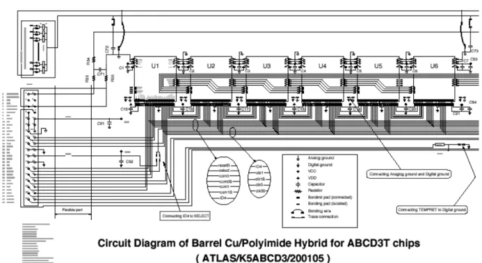
The dimensions of the SCT barrel hybrid are displayed in Fig. 6. The electrical schematics are shown in Fig.
7 and Fig. 8, where Fig. 7 is for the 6 chips on the top side of the module, link0, and Fig. 8 for the 6 chips on the bottom side of the module, link1. Each link has one master chip, which is responsible for the transmission of data off the module. The last chip of a link is set to an end function, and the rest of the chips are set to a slave function. The data and tokens are passed between the adjacent chips with "datain0/dataout0" and
"tokenout0/tokenin0" pads at the back-end of the chips (Fig. 5). In the case of a failure, a chip is skipped by using the "datain1/dataout1" and "tokenout1/tokenin1" pad connections at its side. The digital and analogue ground connections are made on the hybrid, at the side of every ASIC.
The hybrid is made of four copper layers, whose functions are summarized in Table 5. The middle two layers, L2 and L3, extend through the flexible circuit from the connector to the far-end of the hybrid, and L3 is continuous to make the resistivity of the grounds as small as possible. The thickness of the copper is 12 μm.
The ground and power planes of layers L1 and L4 are meshed with 50% openings to compensate for an increase in material from the metallization of through-holes and vias causing thickening to 30 μm. The thickness of the flexible circuit at the hybrid section is 280 μm.
Fig. 6: Dimensions (in mm) of the SCT barrel hybrid
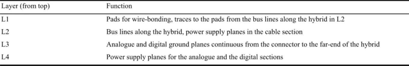
Table 5: Function of each of the four Cu layers of the SCT barrel hybrid
Layer (from top) Function
L1 Pads for wire-bonding, traces to the pads from the bus lines along the hybrid in L2 L2 Bus lines along the hybrid, power supply planes in the cable section
L3 Analogue and digital ground planes continuous from the connector to the far-end of the hybrid L4 Power supply planes for the analogue and the digital sections
Fig. 7: Circuit diagram of SCT barrel hybrid (connector and link0 circuitry)
Fig. 8: Circuit diagram of the SCT barrel hybrid (link1)
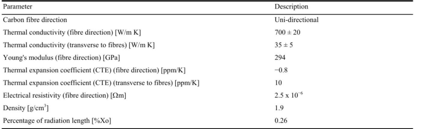
The Cu/Polyimide flexible circuit is reinforced with a bridge to provide good thermal conductivity and high Young's modulus, with only a small fraction of a radiation length of material. The bridge substrate is made of carbon-carbon material with uni-directional fibres along the length of the hybrid to maximize the thermal conductivity. It is connected electrically to the ground of the hybrid and ASICs. The properties of carbon-carbon are summarized in Table 6 and the specification of the bridge is shown in Fig. 9. The surface of the bridge is coated with a polymer, Parylene, to a thickness of 10 μm, to provide insulation and improve reliability for handling. The surface of this coating is roughened with a laser where adhesion is required, and the coating is removed where electrical and thermal conduction are necessary.
The pitch of the input pads of the ASIC is 48 μm, whereas that of the silicon microstrip sensors is 80 μm. In order to make simple parallel wire-bonding, a pitch-adapter is used in front of the ASICs. Because of the fine pitch, the pads and traces are fabricated on a glass substrate with a thin aluminium deposition. The size of the pitch adapter is 63 mm (long) x 2.7 mm (wide) x 0.2 mm (thick). The thickness of aluminium is in the range 0.9 μm to 1.0 μm. The fabrication details for the pitch-adapter are described in [15].
In order to transfer the heat from the ASICs and to connect their ground to the carbon-carbon bridge, a set of 17 through-holes per chip is placed in the hybrid ASIC analogue section. The through-holes are 300 μm in diameter, plated with Cu of 20 μm thickness, and filled with silver-loaded electrically conductive adhesive. The effective thermal conductivity of these "pillars" is estimated to be about 40 W/m K.
Two thermistors, one per link, are equipped to monitor the temperature of the hybrid. The temperature is readily calculated from the measured resistance, R, as
R = R25 exp(B(−1/T+1/T25)) (1) where the temperature, T, is given in Kelvin and R25 and T25 are the nominal resistance and the temperature (in
Kelvin) at 25 oC, respectively. The thermistors have R25 = 10 kΩ ± 1% and B = 3435 K ± 1%.
2.3
72.9 74.6±0.2
8.9 7.5 21±0.1
0.8 ± 0.05
4±0.2 (66.6) 4±0.2
2-ø1.8
(1.74)
T=0.30±0.03 11.7
4 10.24
5x10.24=51.2 11.7
2 5.6
Openings for electrical contact 6 - 2 mm x 4 mm
Surface roughened 21mm x 74.6 mm
Surface roughened 2 sections 2 - 4 mm x 21 mm
Fig. 9: Specification of the hybrid carbon-carbon bridge (dimensions in mm).
Table 6: Properties of the hybrid carbon-carbon substrate material
Parameter Description
Carbon fibre direction Uni-directional
Thermal conductivity (fibre direction) [W/m K] 700 ± 20
Thermal conductivity (transverse to fibres) [W/m K] 35 ± 5
Young's modulus (fibre direction) [GPa] 294
Thermal expansion coefficient (CTE) (fibre direction) [ppm/K] −0.8 Thermal expansion coefficient (CTE) (transverse to fibres) [ppm/K] 10
Electrical resistivity (fibre direction) [Ωm] 2.5 x 10⁻⁶
Density [g/cm3] 1.9
Percentage of radiation length [%Xo] 0.26
2.2.5 Adhesives
The barrel modules are constructed from the four major components described above; the silicon microstrip sensors, baseboards, ASICs and hybrids. They are joined together with thermally conductive and electrically conductive epoxy adhesives. Epoxy adhesives are chosen since they are known to be radiation-tolerant up to a very high fluence.
A thermally conductive adhesive is required in order to transfer the heat generated in the sensors into the baseboard. This is critical, especially after accumulating a large fluence of particles which damage the silicon bulk and induce an increase of many orders of magnitude in the leakage current, together with increased full depletion voltage. The sensors may run away thermally through positive feedback of the leakage current and the temperature unless the heat from the sensors is transferred to the baseboard efficiently. Thermally conductive epoxy is also used for other joints where thermal conduction is required, such as the attachment of the hybrid to the beryllia facings of the baseboard (section 2.2.2).
An electrically conductive epoxy is required because the baseboard, made of carbon, is used for the electrical conductive path from the bias line on the hybrid to the backplane of the sensors. The readout ASICs are also attached to the hybrids with electrically conductive epoxy.
The thermally conductive epoxy used is a two part, room temperature curing epoxy, known as Araldite 2011 [16]. In order to enhance its thermal conductivity, a boron-nitride (BN) filler is added [17]. Boron-nitride was chosen in preference to alumina for this filler as tests with alumina showed that some increase was caused in the leakage current of the glued sensors. The resin, hardener and filler are mixed by weight in the proportions 38.5%, 30.75% and 30.75%, respectively. The thermal conductivity of the mixture is estimated to be about 1 W/m K.
The electrically conductive epoxy used is a two part, low temperature curing epoxy, Eotite p-102 [18].
Although the listed curing temperature is above 50 oC for this product, the epoxy will cure at room temperature after sufficient time (for example, 24 h at 23 oC).
2.3. Specifications for the assembled module
2.3.1. Mechanical specification
Each barrel module contains four 63.96 mm x 63.56 mm (cut-edge to cut-edge) single-sided silicon microstrip sensors. The geometrical alignment of the two sensors on one side, to form a 128 mm long unit, is shown in Fig. 10. The strips of the two sensors are wire-bonded to form 126 mm long strips in a later stage of the assembly (section 3.2.4). The pitch of the strips is 80 µm and there are physically 770 strips, with the first and the last being connected to the strip bias potential for electric field shaping and for defining the strip boundary.
The sensors have been designed to have a minimum guarding region around their edges, consistent with their high voltage performance requirements. The distance between the sensor cut edge and sensitive region is 1 mm (section 2.2.1), which results in a dead region of ~2 mm length in the centre of the module.
Some principal barrel module parameters are summarized in Table 7. The sensors and hybrid on the two sides are rotated around the "module physics centre", by ± 20 mrad. The "module physics centre" is the geometrical centre of the four sensors. The support structure of the module on the barrel cylinder rotates the module around the "module physics centre" by a further ± 20 mrad so that strips on one side of the module are parallel to the axis of the barrel cylinder and those on the other side are at ± 40 mrad to the axis, the sign alternating for successive barrels.
The nominal thicknesses of the module are: 1.15 mm in the sensor area, 0.93 mm in the beryllia facing area, 3.28 mm in the blank hybrid area, 6.28 mm in the highest hybrid component area, 4.48 mm in the ASIC area, and 5.08 mm in the highest wire-bond area. Since wire-bonds have height variations, at least a 1 mm stay-clear distance is required in elevation, and so the module stay-clear thickness in the highest wire-bond area is 7.08 mm.
The wrap-around part of the hybrid interconnect cable extends to a distance of between 40.0 mm and 41.22 mm from the module centre, depending on the shape at the wrap-around.
63.560 61.440
63.960 62.000
63.960 62.000 126
0.130
Fig. 10: Geometrical alignment of the two silicon microstrip sensors in the SCT barrel module. The shading represents their sensitive area.
Units are in mm.
Table 7: Some SCT barrel module mechanical, electrical and thermal specifications Parameter Description Silicon outer dimension 63.56 mm x 128.05 mm (cut-edge)
Construction Four 63.56 mm x 63.96 mm p-in-n single-sided sensors to form back-to-back glued sensors
Mechanical alignment tolerance back-to-back: < 8 μm (in-plane lateral, X), < 20 μm (in-plane longitudinal, Y), < 70 μm (out-of-plane, Z, deviation from the average profile)
Fixing point: < 40 μm (X), < 40 μm (Y) Strip length 126.09 mm (2.090 mm dead in the middle) Strip directions ±20 mrad (0, ±40 mrad on support structure) Number of readout strips 768 per side, 1536 total
Strip pitch 80 μm
Hybrid one-piece hybrid wrapped around the module
Hybrid power consumption 5.5 W nominal, 7.5 W maximum
Maximum sensor bias voltage 460 V (on the detector), up to 500 V in the module Operating temperature of sensor −7 oC (average)
Uniformity of silicon temperature < 5 oC Maximum irradiated sensor power
consumption
1 W total at −7 oC, Heat flux (285 µm): 120 µW/mm2 at 0oC
There is a maximum error of about 500 µm in the connector position on the hybrid ‘pigtail’ cable (Fig. 2), coming from both the error in the connector placement within the hybrid and that of the hybrid placement in the module. The flexible pigtail cable has to connect to a less flexible opto-harness on the barrel cylinder [19].
The hybrid pigtail cable is sufficiently long to allow its route to be adjusted to achieve the correct mating between the two connectors.
The cut edge of the sensor is conductive and at the high voltage of the backside of the sensors. Thus conducting debris between the cut edge and ground could cause high voltage shorts. A stay-clear distance of at least 1 mm is imposed between the sensor edge and any other ground potential when the module is mounted on the barrel, which assures a high voltage breakdown of 3 kV to ground at sea level in air [20]. The centres of adjacent modules are separated by 2.8 mm in height on the cylinders. This distance leaves a nominal stay-clear distance of 1.65 mm between a cut edge and the opposing sensor surface, after allowing for 400 μm in thickness tolerances and 200 μm in non-planarity tolerance of overlapping modules.
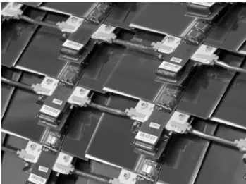
The layout of modules mounted on a barrel is illustrated in Fig. 11. The visible features include the overlap of the silicon of neighbouring modules, the stereo angle of the lower silicon sensors within a module and the hybrid pigtail connection.
Fig. 11: A photograph of modules mounted on a barrel cylinder. The large beryllia facings of the modules are connected mechanically by PEEK clips and thermally by grease to heat sinks, which are aluminium blocks with copper-kapton shunt-shields, soldered to the visible Cu/Ni cooling pipes (which have 70 μm wall thickess).
2.3.2. Thermal Specification
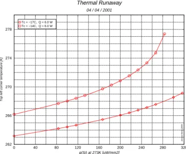
The module design must be safe against thermal runaway of the silicon sensors throughout the lifetime of the SCT. The requirement is also to maintain the sensors at a uniform temperature of about –7 0C to reduce the reverse annealing of the silicon and the bulk leakage current after radiation damage (section 2.1). The module design was therefore developed with the help of thermal Finite Element Analysis (FEA) simulations. The bulk heat generation after 10 years of operation at LHC is estimated to be 120 µW/mm2 at 0 oC in the silicon microstrip sensors in the worst case (Table 7). The calculated thermal profile of the module is shown in Fig. 12 for a hybrid power consumption of 6.0 W and a heat sink temperature of –14 oC at the cooling contact (which is the large beryllia facing that contacts the cooling block on a barrel, Fig. 11, through thermal grease and a copper-kapton shunt-shield). The highest temperature of the module is at the ASIC in the middle of the hybrid, and is about 20 oC above the heat sink temperature. The maximum (Tsimax) temperature of the silicon sensors is about 10 oC above the heat sink temperature, at the top left corner of the sensor. The Tsimax temperature as a function of the bulk heat generation, normalized at 0 oC, is shown in Fig. 13 for a hybrid power consumption of 6.0 W and heat sink temperatures of –14 0C and –17 oC. The simulation shows that thermal runaway of the silicon sensor would occur at 280 µW/mm2 at −14 oC heat sink temperature, which gives a safety factor of 2.3 against thermal runaway for the estimated final heat generation of 120 µW/mm2. For a hybrid power consumption of 8 W, in excess of the anticipated maximum of ~ 7.5 W, a slightly lower heat sink temperature of –17 oC is required to give a similar safety factor, with thermal runaway at 290 µW/mm2. A temperature of –17
oC at the module cooling interface can be achieved by operating the SCT evaporative cooling system at –25 oC, which is within its design specification.
2.3.3. Mass specification
The module has to be designed to minimize the material presented to particles. The target figure within the initial overall ATLAS detector design was 1.2% of a radiation length, averaged over the module area, for particles at normal incidence to the silicon [3]. The calculated radiation length fractions and masses of the components for the final module design are summarized in Table 8. The actual weights of components have been measured and the results match the estimated values to within a few percent. The maximum contribution comes from the silicon sensors, and their thickness was reduced from a standard 300 µm to 285 µm (section 2.2.1) to reduce the material budget (and also the full depletion voltage). The overall mass of the module is 25 g and the percentage radiation length averaged over the silicon sensor area is 1.17% Xo. This therefore matches the ATLAS requirement for the module. The total material in the as-built SCT barrel detector averages ~3% Xo
per layer, and is dominated by the module services.
Fig. 12: An FEA simulation of the thermal profile of the SCT barrel module, with the maximum heat generation in the silicon microstrip sensors, 120 μW/mm2, a hybrid power consumption of 6 W, and a heat sink temperature of –14 0C at the cooling contact. The highest and the lowest temperatures are +5.7 0C and –13.8 0C, respectively.
0 40 80 120 160 200 240 280 320
q(Si) at 273K [uW/mm2]
262 266 270 274 278
Top left corner temperature [K]
Thermal Runaway
04 / 04 / 2001
Tc = −17C, Q = 6.0 W Tc = −14C, Q = 6.0 W
Jerome Morin,QMW
Fig. 13: Temperature of the hottest point in the sensors as a function of heat generation for a hybrid power of 6 W, with the heat sink temperatures of –14 0C (upper curve) and –17 0C (lower curve).
Table 8: Radiation length percentages and masses estimated for the SCT barrel module Component Percentage of a radiation
length [%Xo]
Mass [g] Fraction of total module mass [%]
Silicon sensors and adhesives 0.612 10.9 44
Baseboard and BeO facings 0.194 6.7 27
ASICs and adhesives 0.063 1.0 4
Cu/Polyimide/CC hybrid 0.221 4.7 19
Surface mount components 0.076 1.6 6
Total 1.17 24.9 100
2.3.4. Electrical performance
The criteria for the module to be classified as electrically good are shown in Table 9. The strip
‘micro-discharge’ criterion relates to the fact that the anticipated radiation levels during ATLAS running are a factor of two larger for Barrel 3 than for Barrel 6. After 10 years of ATLAS operation (with the LHC as presently approved) and the corresponding radiation damage and type inversion of the silicon sensors, it is expected that the modules on Barrel 3 will need to be operated at ~ 450 V bias for ~90% charge collection efficiency, while those on Barrel 6 will operate at ~ 250 V bias. The initial operation within ATLAS is expected to be at 150 V bias for all barrels. The electric field configuration and high voltage properties of sensors are different after type inversion following irradiation. All SCT sensors are specified to operate up to 500 V post-irradiation (section 2.2.1), without strip micro-discharge breakdown [6] and this has been verified by sampling measurements. The initial sensor leakage currents on delivery are, however, specified only up to 350 V, and ~ 1.5 % of sensors have some micro-discharge between 350 V and 500 V in their initial state. This micro-discharge arises from the initial high electric field region close to the edges of the implanted strips in the sensors causing local breakdown, which rapidly decays with time, the plateau value of the current being similar to that for a normal sensor. The definition of acceptable micro-discharge (as opposed to other mechanisms, such as bonding damage, resulting in high currents) used by the SCT is that the current approaches a plateau of less than 1 µA within an hour when held under bias at the onset of the micro-discharge voltage.
The presence of micro-discharge between 350 V and 500 V bias has no implication for the operation of a module at the initial bias of 150 V within ATLAS. However, modules need to be tested during the assembly of the SCT up to their final bias voltage anticipated after 10 years of ATLAS operation to ensure that there is no high voltage breakdown coming, for example, from conducting debris shorting to ground. Thus the modules are grouped into two electrical categories on the basis of their leakage current characteristics:
(a) Good for any Barrel - modules with good IV characteristics (module leakage current for the sum of the four sensors versus bias voltage) up to 500 V bias after construction, which can therefore be tested initially for HV integrity up to 500 V and so are suitable for mounting on the innermost barrels.
(b) Good for Barrel 5 or Barrel 6 – modules with good IV characteristics up to 350 V (the sensor specification) after construction, but with micro-discharge between 350 V and 500 V. They are not tested for HV integrity above 350 V after mounting on the barrel, and so are suitable for Barrels 5 or 6, where the operating voltage in ATLAS is never expected to exceed 350 V. (In practice, all modules selected for mounting on Barrel 5 could be operated up to 400 V, section 5.)
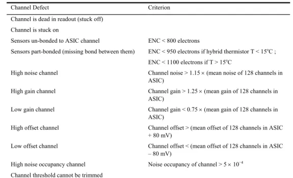
The criteria in Table 9 relating to bad readout channels are based on the definitions of such channels listed in Table 10.
It should be noted that the excellent quality of the sensors with respect to bad channels and leakage current allow limits to be placed on the modules that are considerably tighter than those indicated by the contractual sensor specification (Table 2).
With the ASICs powered, the difference in the thermistor temperatures on the two sides of the hybrid was required to be < 2 0C for a module to be accepted for Barrels 3, 4 or 5. This was a check that the hybrid was properly glued to the beryllia baseboard facings, with a good thermal interface (section 3.2.3). For Barrel 6, the