Prepared for submission to JINST
18thInternational Workshop on Radiation Imaging Detectors 2-6 July 2017
Krakow, Poland
Performance of irradiated thin n-in-p planar pixel sensors for the ATLAS Inner Tracker upgrade
N. Savić,1,aJ. Beyer,a B. Hiti,b G. Kramberger,b A. La Rosa,aA. Macchiolo,aI. Mandić,b R.
Nisius,aM. Petekb
aMax-Planck-Institut für Physik (Werner-Heisenberg-Institut), Föhringer Ring 6, 80805 München, Germany
bJožef Stefan Institut,
Jamova 39, 1000 Ljubljana, Slovenia E-mail: Natascha.Savic@mpp.mpg.de
Abstract: The ATLAS collaboration will replace its tracking detector with new all silicon pixel and strip systems. This will allow to cope with the higher radiation and occupancy levels expected after the 5-fold increase in the luminosity of the LHC accelerator complex (HL-LHC). In the new tracking detector (ITk) pixel modules with increased granularity will implement to maintain the occupancy with a higher track density. In addition, both sensors and read-out chips composing the hybrid modules will be produced employing more radiation hard technologies with respect to the present pixel detector. Due to their outstanding performance in terms of radiation hardness, thin n-in-p sensors are promising candidates to instrument a section of the new pixel system.
Recently produced and developed sensors of new designs will be presented. To test the sensors before interconnection to chips, a punch-through biasing structure was implemented. Its design was optimized to decrease the possible tracking efficiency losses observed. After irradiation, they were caused by the punch-through biasing structure. A sensor compatible with the ATLAS FE-I4 chip with a pixel size of 50x250µm2, subdivided into smaller pixel implants of 30x30µm2 size was designed to investigate the performance of the 50x50µm2pixel cells foreseen for the HL-LHC.
Results on sensor performance of 50x250 and 50x50µm2pixel cells in terms of efficiency, charge collection and electric field properties are obtained with beam tests and the Transient Current Technique.
Keywords: Radiation-hard detectors; Particle tracking detectors, Solid state detectors
1Corresponding author.
Contents
1 ATLAS pixel detector upgrade for HL-LHC 1
2 Characterization of thin n-in-p planar pixel sensors 2
2.1 The Edge Transient Current Technique 2
2.2 Charge collection properties 3
2.3 Electric field properties 4
2.4 Efficiency of 100 and 150µm thick sensors after exposure to high irradiation 6 3 Performance of irradiated sensors with small pixel cells 6
4 Conclusions 7
1 ATLAS pixel detector upgrade for HL-LHC
In view of the high luminosity phase of the LHC (HL-LHC) starting around 2025 the ATLAS experiment will undergo a major upgrade of its tracker system. The ATLAS pixel system is expected to be exposed to fluences up to 1.4×10¹⁶neq/cm2(1 MeV neutron equivalent) [1] taking into account one replacement and including a safety factor of 1.5. To be able to maintain the performance in the new and more challenging environment different technologies are developed to improve radiation hardness and maintain a similar occupancy as in Run 2 despite a higher track density. The baseline technology for all pixel layers except the innermost one is based on pixel modules assembled with thin planar n-in-p sensors. The modules investigated in this paper consist of 100µm and 150µm thick sensors produced at CiS (Germany). The sensors are interconnected with solder bump-bonding to ATLAS FE-I4 read-out chips. Bare sensors are characterized by means of the Edge Transient Current Technique (Edge-TCT) at the Jožef Stefan Institut (JSI) allowing to study the profiles of drift velocity, charge collection and electric field inside heaviliy irradiated silicon detectors to understand the charge transport process in these devices. Sensors from the same production are assembled into modules measured with particle beams at the CERN-SpS. The results of Edge-TCT measurements are discussed for thin either unirradiated or irradiated sensors up to an irradiation level of 1×10¹⁶ neq/cm2. Previous results on the hit efficiency and power dissipation revealed that modules with thin sensors are a promising candidate for the innermost layers [2].
Given the high particle rate expected at HL-LHC smaller pixel dimensions with respect to the ones currently implemented in the FE-I3 chip (50x400µm2) [3] and the FE-I4 chip (50x250µm2) [4] are necessary to keep the occupancy at an acceptable level. The new read-out chip for the future ATLAS pixel system with a pixel cell of 50x50µm2produced in 65 nm CMOS technology is being developed by the CERN RD53 Collaboration [5] and the first prototype, the RD53A chip, is foreseen to be ready by the end of 2017 [6]. At CiS sensors were produced with 50x50µm2pixel cells, connected by a metal layer in such a way to be still compatible with the FE-I4 chip footprint.
Results on the in-pixel efficiency of small pixel implants before irradiation were previously shown in [2] and will now be shown after an irradiation up to 5×10¹⁵neq/cm2.
2 Characterization of thin n-in-p planar pixel sensors
A production of thin planar n-in-p pixel on 4-inch wafers of p-type FZ silicon was recently completed at CiS1. The wafers were locally thinned below each single structure from a starting thickness of 500µm to an active thickness of 100µm or 150µm by using anisotropic Potassium Hydroxide (KOH) etching creating backside cavities in the wafer. This technology does not require handle wafers during the thinning process, thus it is potentially cheaper than the alternative method employing SOI wafers. A more detailed description of the production process is given in Ref. [7].
The standard FE-I4 pixel pitch with a 50x250µm2cell was implemented together with the common punch-through design which was found to retain the highest efficiencies after irradiation [7].
2.1 The Edge Transient Current Technique
The Transient Current Technique with the laser beam pointing at the sensor edge is a powerful method to get insights into the charge collection and electric field properties across the sensor depth. The extraction of the charge collection and velocity profile is based on the measurement of time evolution of the induced current pulse. The technique is known as Edge-TCT and a detailed description can be found in Ref. [8]. In Edge-TCT an infra-red laser with an approximate beam FWHM of 8-12µm and a long penetration depth in silicon of over 1 mm is shining on the edge of the device, a thin bare sensor of 100µm or 150µm thickness, and scanned along the sensor depth and the long direction of the pixel. Charge carriers, electron/hole pairs, are released inside the sensor traversing to their corresponding electrodes. An electrical signal created by the movement of the charge carriers is amplified with an external current amplifier.
(a) (b)
Figure 1. Outlined description of the Edge-TCT set-up fromParticulars[9]: (a) schematics of the experi- mental set-up [10] and (b) detector side view with the laser beam penetrating at the detector edge.
1https://www.cismst.org
All pixels on the frontside are connected to high voltage via a wire bond attached to the bias ring surrounding the pixels, while the backside is set to ground. One single pixel is connected to readout via an additional wire bond. The device is mounted onto a copper support, which is thermally stabilized at room temperature in the case of no irradiation and cooled to -20◦C via a Peltier Cooler when irradiated. The schematics of the Edge-TCT measurement set-up is shown in Fig.1.
2.2 Charge collection properties
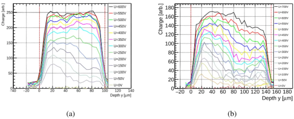
The collected charge is defined as the time integral of the induced current where, in this work, the integration time is chosen to be 10 ns. As depicted in Fig.1the laser beam is moved in steps along the edge of the sensor. With this methodology, charge collection as a function of detector depth can be measured. In this section the results of 100µm or 150µm thick sensors are shown after an irradiation with neutrons in the TRIGA nuclear reactor of JSI [11] up to a fluence of 1×10¹⁶ neq/cm2. After irradiation, the sensors are annealed for 80 min at 60◦C to complete the short term annealing of electrically active defects [12]. In Fig.2 the charge collection as a function of the sensor depth is summarised for voltages from 0 to 700 V. Sensor front and back side are highlighted with the red dashed lines. The sensor front side is represented by the left line. The laser beam is directed to the middle of the pixel implant. The charge is listed in arbitrary units, meaning that the charges are comparable within one set of measurements with the same sample and experimental conditions but not across different samples. This is due to the fact that the absolute value of the current is dependent on the exact laser focus and power as well as the properties of the sensors edge surface. In Fig. 2a the charge is collected through the entire detector thickness already at a bias voltage of 50 V although the detector is irradiated to very high fluences of 1×10¹⁶ neq/cm2 and only a very thin depleted layer is expected at this bias voltage when assuming a constant effective doping concentration Ne f f [13]. This is in agreement with the observation from Ref. [13] that at very high irradiation fluences the electric field is present in the entire detector volume already at low bias voltages. This is explained by space charge polarization and low free carrier concentration in highly irradiated material. The space charge polarization also results in the so called "double peak" effect [15] visible in Fig.2b. The higher charge with respect to the central region is collected at the backside of the device at around 250 V.
µm]
Depth y [
−40 −20 0 20 40 60 80 100 120 140
Charge [arb.]
0 50 100 150 200 250
U=600V U=550V U=500V U=450V U=400V U=350V U=300V U=250V U=200V U=150V U=100V U=50V U=0V
(a)
µm]
Depth y [
−20 0 20 40 60 80 100 120 140 160 180
Charge [arb.]
0 20 40 60 80 100 120 140 160
180 U=700V
U=650V U=600V U=550V U=500V U=450V U=400V U=350V U=300V U=250V U=200V U=150V U=100V U=50V U=0V
(b)
Figure 2. The charge collection as a function of sensor depth is shown for a 100 (a) and 150µm (b) thick sensor after an irradiation at 1×10¹⁶neq/cm2.
µm]
x [
50 100 150 200 250
m]µDepth y [
0 20 40 60 80 100 120 140
Charge [arb]
−20 0 20 40 60 80 100 120 140 160
(a) U=200 V, d=100µm
µm]
x [
0 50 100 150 200 250 300
m]µDepth y [
0 20 40 60 80 100 120 140
Charge [arb]
0 50 100 150 200 250
(b) U=600 V, d=100µm
µm]
x [
50 100 150 200 250
m]µDepth y [
0 20 40 60 80 100 120 140 160
Charge [arb]
−20 0 20 40 60 80 100 120
(c) U=200 V, d=150µm
µm]
x [
50 100 150 200 250
m]µDepth y [
0 20 40 60 80 100 120 140 160
Charge [arb]
0 20 40 60 80 100 120 140 160
(d) U=600 V, d=150µm
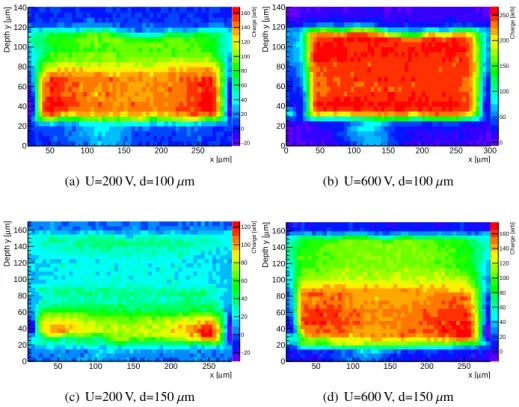
Figure 3. Two-dimensional representation of a charge collection measurement with the Edge-TCT method for one single pixel cell in a 100µm (a,b) or a 150µm (c,d) thick sensor irradiated to 1×10¹⁶neq/cm2, (a,c) at 200 V and (b,d) at 600 V. The collected charge is color-coded.
From 300 V onwards the charge flattens throughout the sensor depth for the 100µm device. For voltages above 450 V no significant change of charge collection is observed, which points to a saturation of the drift velocity. Due to a lower electric field in thicker devices, this effect is not seen for the 150µm thick sensor. It was not possible to apply higher voltages due to limited cooling capabilities. A two-dimensional representation of the charge collection measurement of the 100µm and 150µm thick sensors is depicted in Fig.3. The laser beam direction is impinging perpendicular to the X-Y plane. The sensor front side is at lower y-values with a pixel cell size of 250µm in x.
The depth of the sensor is along the y-axis with the detector surface being at about y=20µm. Red areas represent high charges and the blue colour corresponds to low charges. The negative charge is a contribution from charges generated in the read-out pixel but collected from the adjacent one.
The small charge measured at low y values (i.e when the laser beam is below the detector surface) is caused by light reflection of the wire bond on the read-out pixel. The high charge region at the sensor front side is increasing with voltage for both sensor thicknesses. Comparing both sensors reveals that in the 100µm thin sensor the high charge region extends deeper both at 200 and 600 V.
2.3 Electric field properties
According to Ramo’s theorem [14], the movement of charges inducing a currentI on the read-out pixel can be approximated in the case of a short laser pulse in the Edge-TCT configuration by:
I(y) =q·N ·~v(y)/D (2.1)
whereqis the electric charge of the carrier, N the number of carriers created at depth y,~v(y) the carrier velocity andDthe detector thickness. The term 1/Drepresents the weighting field term for the Edge-TCT set-up with uniform charge generation underneath several adjacent pixels [8].
µm]
Depth y [
−20 0 20 40 60 80 100 120 140 160
Velocity [arb]
10 20 30 40 50 60 70 80
90 U=100V
U=90V U=80V U=70V U=60V U=50V U=40V U=30V U=20V U=10V U=0V
(a) d=100µm
µm]
Depth y [
0 50 100 150 200
Velocity [arb]
0 20 40 60 80 100
120 U=120V
U=110V U=100V U=90V U=80V U=70V U=60V U=50V U=40V U=30V U=20V U=10V U=0V
(b) d=150µm
µm]
Depth y [
−20 0 20 40 60 80 100 120 140 160
Velocity [arb]
0 50 100 150 200
250 U=550V
U=500V U=450V U=400V U=350V U=300V U=250V U=200V U=150V U=100V U=50V U=0V
(c) d=100µm,Φ=5×10¹⁵neq/cm2
µm]
Depth y [
−20 0 20 40 60 80 100 120 140 160
Velocity [arb]
0 50 100 150 200 250
U=600V U=550V U=500V U=450V U=400V U=350V U=300V U=250V U=200V U=150V U=100V U=50V U=0V
(d) d=100µm,Φ=1×10¹⁶neq/cm2
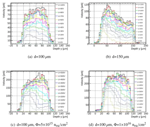
Figure 4. Velocity profile as a function of sensor depth for not irradiated 100µm (a) and 150µm (b) thick sensors and for a 100µm thick sensor after an irradiation to 5×10¹⁵neq/cm2 (c) and 1×10¹⁶ neq/cm2 (d).
The values of the velocity correspond to arbitrary units.
If measured immediately after the pulse, before the carriers drift away from the location of the laser beam,~v(y)is the velocity sum of the holes and electrons at depthy. Hence, it is possible to obtain the velocity profile from the increase of the signal in the very first ns. From the velocity profile the shape at the electric field can be inferred. In Fig.4the velocity profiles of not irradiated 100µm and 150µm thick sensors are compared. A higher carrier velocity at the front side at lower voltages is observed for both thicknesses. At higher voltages the distribution is flatter for the 100µm thick device, both before and after irradiation due to a more uniform electric field in thinner devices.
The existence of the electric field at the back side of the sensor results in the devices to be fully depleted at 10 V in case of the 100µm detector and at 20 V for the 150µm thick detector. The velocity profiles after irradiation confirm the above hypothesis that an electric field in the entire sensor thickness already exists at low bias voltages. A double peak electric field distribution can be seen for both sensor thicknesses at low moderated bias voltage below 200 V, but the field flattens at higher bias voltages. However, the electric field at the back is much weaker with respect to the electric field at the main junction of the pixels. The double peak effect after irradiation for thicker sensors has been reported in several publications [15].
2.4 Efficiency of 100 and 150µm thick sensors after exposure to high irradiation
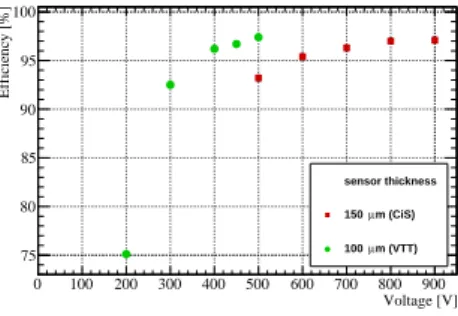
An FE-I4 module employing the 150µm thick sensor irradiated to a fluence of 1×10¹⁶ neq/cm2 is measured with particle beams at CERN. The results are compared to those of an FE-I4 module with a 100µm thick sensor previously reported in [2]. The systematic uncertainty associated to the efficiency measurements is 0.3% [16]. In Fig.5for 500 V the hit efficiency of the 100µm device of 97.4% is higher than the efficiency of the 150µm sensor. The efficiency of the module with a 150µm thick sensor saturates at a similiar value of 97.0% with the significant difference being the higher bias voltage of around 800 V needed to achieve the saturation. These results support the charge collection results obtained from Edge-TCT measurements and demonstrate the feasibility of instrumenting the innermost pixel layers at HL-LHC with 100µm thin planar sensors.
Voltage [V]
0 100 200 300 400 500 600 700 800 900
Efficiency [%]
75 80 85 90 95 100
sensor thickness
m (CiS) µ 150
m (VTT) µ 100
Figure 5. Hit efficiencies of FE-I4 modules with 100µm or 150µm thick sensors irradiated to 1×10¹⁶ neq/cm2at JSI in Ljubljana and the PS at CERN. The uncertainties are smaller than the marker size.
3 Performance of irradiated sensors with small pixel cells
For smaller pixels cells of 50x50µm2 a more prominent effect of charge sharing is expected compared to larger pixel cells. A modified 50x250µm2 pixel cell composed of five 30x30 µm2 pixel implants with a 50µm pixel pitch in both directions was designed to investigate the charge sharing in adjacent 50x50µm2 pixels. The implants are connected by metal lines allowing for the readout by the FE-I4 chip. Neigbouring pixel implants are read-out by different channels. A sketch of the design of the modified pixel cell, and a comparison to the standard pixel cell, are displayed in Fig. 6. Before irradiation, no significant effect of charge sharing among neighbouring pixels is observed on the hit efficiency although the charge would be splitted between two adjacent pixel readout channels [2]. This is due to the fact that the charge in the pixel cell is still above threshold, thus not affecting the efficiency. After irradiation the effect of charge sharing for smaller pixel cells is evident at lower bias voltages. The in-pixel efficiency maps after an irradiation to 3 and 5×10¹⁵neq/cm2are shown in Fig.7for the sensors biased at 300 V and 500 V (a) and at 500 V and 600 V (b). At a fluence of 3×10¹⁵neq/cm2and at a bias voltage of 300 V the hit efficiency is lower between the pixel implants. At a higher bias voltage of 500 V the efficiency is more uniform across the unit cell. The highlighted 50x50µm2pixel cell is chosen to be the closest approximation to the geometry of RD53A compatible pixel cells without punch-through structure. It is surrounded by eight pixel cells, where seven of them are readout by different readout channels, only one is read out by the same channel. In these conditions, a hit efficiency of 98.2% was estimated for a 50x50 µm2
cell of 150 µm thickness without any biasing structure (Fig.7(b, top)), whereas at a higher fluence of 5×10¹⁵ neq/cm2 and at 600 V the hit efficiency was calculated to be 97.5% for a 100µm thick sensor (Fig.7(b, bottom)). With this modified geometry of the FE-I4 compatible sensor design first predictions on the performance of 50x50µm2pixel cells after irradiation can be made.
Figure 6. A modified 50x250µm2pixel cell composed of five 30x30µm2pixel implants with a 50µm pixel pitch in both directions is shown and compared to a standard pixel cell. The implants are connected by metal lines allowing for readout by the FE-I4 chip. In both structures the common punch-through is implemented.
m]
µ Long Side [
0 50 100 150 200 250
m]µShort Side [
0 20 40 60 80 100
0.75 0.8 0.85 0.9 0.95 1
m]
µ Long Side [
0 50 100 150 200 250
m]µShort Side [
0 20 40 60 80
0.75 0.8 0.85 0.9 0.95 1
(a)
m]
µ Long Side [ 200 205 210 215 220 225 230 235 240 245
m]µShort Side [
0 5 10 15 20 25 30 35 40 45
0.8 0.82 0.84 0.86 0.88 0.9 0.92 0.94 0.96 0.98 1
(b)
Figure 7. In-pixel efficiency map for a 150µm thin sensor (top) at 300 V (a) and 500 V (b) irradiated to 3×10¹⁵neq/cm2and a 100µm thin sensor (bottom) at 500 V (a) and 600 V (b) irradiated to 5×10¹⁵neq/cm2. In (a) the scale is zoomed to make the efficiency loss visible in between the pixel cells. In (b) the design is overlayed and the efficiency of the edge implant is calculated as the closest approximation of the geometry of a RD53A 50x50µm2pixel cell without punch-through structure.
4 Conclusions
At CiS 100 and 150 µm thick sensors with standard and modified 50x250 µm2 pixel cells were produced. The thin sensors are characterized by Edge-TCT and beam test measurements. Charge collection and velocity are extracted from Edge-TCT measurements and compared to efficiency results obtained during beam test campaigns. For a 100µm thick sensor the charge collection profiles at all fluences flatten above 350-400 V. The 150µm thick irradiated sensor does not reach this condition given the restriction in the bias voltage caused by limitations of the available cooling system. In the chosen range of bias voltages the electric field is flatter for the 100µm thick sensors with respect to the 150µm thick sensors. An indication of a double peak in the electric field can
only be observed at low bias voltages. Results obtained with particle beams support the Edge-TCT results. A module with a 100µm thick sensor reaches an efficiency of 97.4% at a moderate bias voltage of 500 V. These results show that this technology can be applied in the innermost layers of the HL-LHC pixel systems. Furthermore, modified 50x250µm2pixel cells with 30x30µm2 pixel implants were produced to investigate the performance of the future small pixel cells for the RD53A chip. A 50x50µm2 pixel cell in a 150µm thick sensor after an irradiation to 3×10¹⁵ neq/cm2 is shown to achieve an efficiency of 98.2%, and in the case of a 100µm thick sensor irradiated to 5×10¹⁵neq/cm2an efficiency of 97.5% is observed.
Acknowledgments
This work has been partially performed in the framework of the CERN RD50 Collaboration. The authors thank F. Ravotti for the irradiation at CERN-PS, I. Mandić for the one at JSI, L. Gonella for the one at UoB. Supported by the H2020 project AIDA-2020, GA no. 654168.
References
[1] P. S. Miyagawa and I. Dawson,Radiation background studies for the Phase II inner tracker upgrade, CERN, ATL-UPGRADE-PUB-2013-012 (2013).
[2] N. Savic et al.,Investigation of thin n-in-p planar pixel modules for the ATLAS upgrade, JINST 11 (2016) C12008.
[3] I. Peric,The FEI3 read out chip for the ATLAS pixel detector, Nucl. Instr. Meth. A565 (2006) 178.
[4] M. G.-Sciveres et al.,The FE-I4 pixel readout integrated circuit, Nucl. Instr. Meth. A363 (2012) 29.
[5] RD53 Collaboration,http://rd53.web.cern.ch/RD53/
[6] M. G.-Sciveres et al.,Towards third generation pixel readout chips, Nucl. Instr. Meth. A731 (2013) 83.
[7] N. Savic et al.,Thin n-in-p planar pixel modules for the ATLAS upgrade at HL-LHC, Nucl. Instr. and Meth. A845 (2017) 154.
[8] G. Kramberger et al.,Investigation of irradiated silicon detectors by Edge-TCT, IEEE Trans. Nucl. Sci 57 (2010) 2294.
[9] Particulars, advanced measurement systemshttp://www.particulars.si
[10] I. Mandic et al.,Edge-TCT measurements with the laser beam directed parallel to the strips, JINST 10 (2015) P08004.
[11] M. Ravnik and R. Jeraj,Research reactor benchmarks, Nucl. Sci. Eng. 145 (2003) 145.
[12] G. Lindstroem et al,Radiation hard silicon detectors developments by the RD48 (ROSE) Collaboration, Nucl. Instr. and Meth. A466 (2001) 308.
[13] G. Kramberger et al.,Modeling of electric field in silicon micro-strip detectors irradiated with neutrons and pions, JINST 9 (2015 ) P10017.
[14] S. Ramo,Currents induced by electron motion, Proc. I.R.E. 27 (1939) 584.
[15] G. Kramberger et al.,Electric Field Modeling in heavily irradiated silicon detectors based on Edge-TCT measurements, JINST 9 (2014) P10016.
[16] J. Weingarten et al.,Planar pixel sensors for the ATLAS upgrade, JINST 7 (2012) P10028.
![Figure 1. Outlined description of the Edge-TCT set-up from Particulars [9]: (a) schematics of the experi- experi-mental set-up [10] and (b) detector side view with the laser beam penetrating at the detector edge.](https://thumb-eu.123doks.com/thumbv2/1library_info/4003861.1540703/3.892.203.685.730.1000/figure-outlined-description-particulars-schematics-detector-penetrating-detector.webp)