Thorsten Berstermann
Ultrafast Piezospectroscopy of
Semiconductor Micro- and Nanostructures
Ultrafast Piezospectroscopy of
Semiconductor Micro- and Nanostructures
Dissertation
presented to the Faculty of Physics of the Technische Universit¨ at Dortmund, Germany,
in partial fulfillment of the requirements for the degree of Doktor rer. nat.
presented by
Thorsten Berstermann
Dortmund, May 3, 2010
Accepted by the Faculty of Physics of the Technische Universit¨ at Dortmund, Germany.
Day of the oral exam: 8th April 2010 Examination board:
Prof. Dr. Manfred Bayer Prof. Dr. Metin Tolan Prof. Dr. G¨ otz S. Uhrig
Dr. B¨ arbel Siegmann
Contents
I Introduction 1
1 Motivation and Outline 3
2 Picosecond Laser Acoustics 5
2.1 The Phonon Concept . . . . 5
2.2 Coherent Phonons . . . . 7
2.2.1 Excitation of Ultrashort Coherent Phonon Wavepackets . . . . . 7
2.3 Anharmonicity: Shockwaves and Acoustic Solitons . . . . 9
2.3.1 Concept of Strain Energy . . . . 9
2.3.2 Nonlinear Elastic Expansion . . . . 10
2.3.3 Korteweg-de-Vries Equation . . . . 11
3 Semiconductor structures 15 3.1 Optics . . . . 15
3.1.1 Semiconductor Microcavities . . . . 16
3.1.2 Semiconductor Quantum Wells . . . . 19
3.1.3 Principles of Light-Matter Interaction . . . . 21
3.2 Acousto-Optics and Acousto-Opto-Electronics . . . . 24
3.2.1 Semiconductor Microcavities . . . . 24
3.2.2 Semiconductor Quantum Wells . . . . 27
4 Summary and Experimental Prospects 29 II Ultrafast Piezospectroscopy 31 5 Outline and Experiments 33 5.1 Experimental Setup . . . . 33
5.2 Excitation and Detection . . . . 35
6 Optical Bandpass Switching in a Semiconductor Microcavity 37 6.1 Sample and Experiment . . . . 37
6.2 Acoustic Pulse Induced Effects . . . . 39
6.3 Discussion and Analysis . . . . 41
7 Chirping of an Optical Transition in a Quantum Well 47
7.1 Sample and Experimental Conditions . . . . 47
7.2 Strain Modulated Exciton Resonances . . . . 49
7.3 Discussion and Analysis . . . . 53
7.4 Outlook . . . . 55
8 Generation of Terahertz Sidebands in a Planar Quantum Well Cavity 57 8.1 Introduction . . . . 57
8.2 Experiment and Sample . . . . 59
8.3 Diabatic Frequency Modulation . . . . 61
8.4 Model Calculation . . . . 64
8.5 Conclusions and Outlook . . . . 68
9 Manipulation of Light Matter Interaction 69 9.1 Introduction . . . . 69
9.2 Experimental Conditions and Sample . . . . 70
9.3 Results and Discussion . . . . 72
9.4 Summary and Outlook . . . . 77
10 Ultrafast Control of Polariton Emission Dynamics 79 10.1 Introduction . . . . 79
10.2 Strain Modulated Photoluminescense . . . . 81
10.3 Experimental Results . . . . 82
10.4 Conclusions . . . . 86
11 Summary and Future Prospects 87
Bibliography 89
List of Publications 97
Part I
Introduction
1 Motivation and Outline
He who is certain he knows the ending of things when he is only beginning them is either extremely wise or extremely foolish;
no matter which is true, he is certainly an unhappy man, for he has put a knife in the heart of wonder.
Robert Paul Williams
L ight and sound have been daily attendants of mankind from time immemorial since they form the basic tools for interpersonal communication and experiencing nature.
Nowadays optics and acoustics have evolved to be two of the main subjects in physics, still attracting interest of thousands of scientists working on light- and soundrelated phenomena all over the world. Soundwaves have been investigated in a wide frequency range in fields like seismo-
logy, medicine and material science, and have been found to offer a variety of possi- ble applications. The wavelengths thereby cover a range from kilometers down to a nanometer scale, where the latter have led to the field of terahertz acoustics in solids, utilizing vibrations with ultimate wavelengths in the order of the atomic distances.
To obtain information about the vibrational spectra in solids, several techniques have been developed, among of which optical spectroscopy has turned out to be a promising one.
The rapid developement of optical spectroscopy during the last decades was accel-
erated by more and more advanced laser systems available. The diversity of lasers
thereby reaches from spectrally ultranarrow lasers, with linewidths down to Hz at well
defined frequencies to ultrashort laser pulses, with pulse durations down to attoseconds,
both close to constraints given by fundamental laws of nature. This developement was
driven to a high extent by the progress in semiconductor physics, aiming at applications
in the field of communication and information technologies. In particular miniaturized
semiconductor structures, in which quantum effects became directly accessible required
highly sophisticated spectroscopic equipment.
Nowadays, it is possible to taylor the properties of these semiconductor nanostructures to a wide extend, such that it became feasible to study the interaction between various optically, acoustically and electronically well defined nanostructures with the ambition to experience nature on a quantum level and to apply the gained knowledge to every- day life.
This work focuses on the investigation of the impact of acoustic wave packages on the optical properties of semiconductor nanostructures using optical spectroscopy. In particular fast modulation processes will be presented, occuring on timescales compa- rable or even shorter than the typical optical response-, or rather interaction times of the structures under consideration. The experiments make use of a picosecond laser ultrasonics technique to generate the acoustic wave packages, which provide a powerful tool for reaching new acousto-optic and acousto-electro-optic regimes.
In this introductory part I, a reasonable physical background will be given in order to catch on with the physical context presented in part II. Readers who are familiar with the principals of ultrafast acoustics, semiconductor microcavity and quantum well structures as well as with two dimensional cavity polaritons may skip this part.
The introductory part is organized as follows. In Chapter 2 a review over the ba-
sic theoretical aspects of acoustics will be given. As a preface the phonon concept
will be roughly summarized in Chapter 2.1. In Chapter 2.2 the main mechanisms of
the used coherent phonon wavepacket excitation process are presented; its time evo-
lution is discussed in Chapter 2.3, where anharmonicity and dispersion are shown to
lead to distinct regimes concerning acoustic wavepacket propagation. In the subse-
quent Chapter 3 the attention will be on the basic properties of the semiconductor
nanostructures investigated througout this work. In Chapter 3.1 the focus is on the
optical properties of semiconductor Bragg microcavities, quantum wells as well as on
cavity polaritons. In Chapter 3.2 the interaction mechanisms of these structures with
an acoustic wavepacket are described separating acousto-optic and acousto-electro-
optic effects. Chapter 4 comprehends a summary of the theoretical Part I and shows
prospects with regard to possible constitutive experimental implementations.
2 Picosecond Laser Acoustics
G enerally vibrations might occur in all physical systems in which a potential land- scape, which favors a non singular equilibrium state is predominant. If any of theses systems experiences a small perturbation such that the energy of the system is in- creased, it will start to oscillate around its equilibrium state, with frequencies that can be related to the physical properties of the involved objects, as well as to the kind of perturbation.
In the following chapter an introduction will be given concerning lattice vibrations, which might occur in semiconductor crystal structures focusing on longitudinal, coher- ent crystal excitations referred to as coherent longitudinal acoustic phonons. These excitations will act as the key tool in the modulation processes described in Part II and are therefore of particular importance in the context of this work. In detail in Section 2.1 the phonon concept will be reviewed, where the basic idea as well as the most important phonon properties will be highlighted. In the subsequent Section 2.2 the focus will be on the excitation process of picosecond pulses of coherent longitudinal acoustic phonons, forming propagating strain waves. Further in Section 2.3 the mech- anisms of nonlinear and dispersive strain wave propagation will be sketched, leading to shockwave and acoustic soliton formation.
2.1 The Phonon Concept
In order to describe the lattice dynamics in crystals it is convenient to take advantage of the adiabatic approximation, that separates the motion of the ionic cores from that of their valence electrons. Within the adiabatic approximation the electron dynamics are considered to evolve on timescales three orders of magnitude faster than those of the ion cores and can be approximated by the corresponding electronic ground state [1]. Turning now to the lattice dynamics translational symmetrie of the crystal reduces the problem to the unit cell, which includes all necessary information.
Within the unit cell one might only consider two body interactions [2] writing a poten- tial U (R) depending on the separation R of the atomic ion cores, or, simply spoken, the interatomic separation. Expanding this potential in terms of small displacements u = R − R
0from the equilibrium separation R
0, one may write:
U − U (R
0) = u ∂U
∂R
R=R0
+ u
2∂
2U
∂R
2R=R0
+ ... (2.1)
Following Equation 2.1, in second order approximation, the lattice dynamics may be
expressed by a harmonic potential since the linear term vanishes on account of the
Acoustic
Optical
Transverse Longitudinal
Phonon (a)
(c) (d)
(b)
q q
q q
Figure 2.1:
Phonon classification:(a) transverse acoustic phonon (b) longi- tudinal acoustic phonon (c) transverse optical phonon (c) longitudinal optical phonon.
definition of equilibrium. A crystal atom though, in this approximation can be de- scribed by a three dimensional harmonic oscillator, justifying the application of linear force models [1]. The electronic contribution thereby enters the model via the phe- nomenological force constants, whichs physical information might be a nontrivial task to understand [3][4][5].
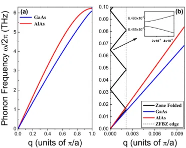
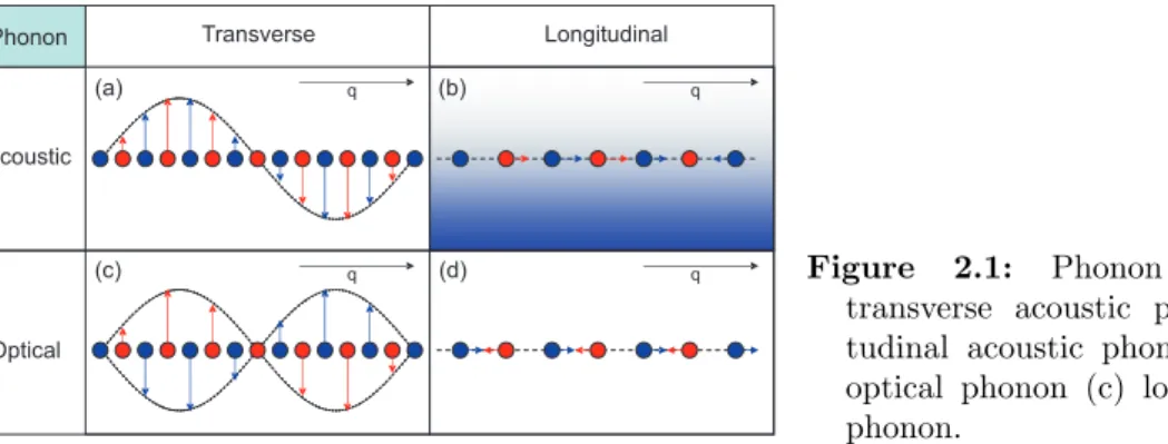
Equation 2.1 can be solved by a travelling wave (r-space, t-time) of the form uexp[i(qr − ωt) + iφ], where q denotes the wave vector, u the amplitude of displacement of the atoms from the equilibrium position, ω is the angular frequency of the wave with el- ementary excitation energy ~ ω, and φ its phase. This crystal excitation is called a phonon and describes collective oscillations of the lattice atoms. In general two classes of phonons excist referred as acoustic phonons and optical phonons, depending on whether the unit cell atoms oscillate in phase or in antiphase. Within these classes a phonon is called transverse, if u ⊥ q or longitudinal, if u k q. Figure 2.1 shows a chart from which all different kinds of phonons can be seen. The occupation of the different phonon states in thermal equilibrium is governed by the Bose-Einstein statis- tics, where the relation between the energies ~ ω and the wave vector q is called the phonon dispersion. A calculated phonon dispersion for a GaAs bulk crystal, based on a one dimensional linear chain model [6][7] is shown in Fig. 2.2. As the model is one dimensional, only longitudinal phonons appear.
-1.0 -0.5 0.0 0.5 1.0
0 1 2 3 4 5 6 7 8 9
PhononFrequency/2(THz)
q (units of /a) GaAs bulk
LO
LA
Figure 2.2:
Real part of the phonon disper- sion in bulk GaAs calculated from a linear chain model [6]: The interatomic force con- stant Λ = 90.7 N/m. Further the atom sepa- ration
a= 2.83 ˚ A, the masses
mGa= 69.723
m, mAs= 74.923
m(m, atomic mass unit).
(LO) longitudinal optical, (LA) longitudinal
acoustic phonon branch. The gaps at both
sides of the dispersion indicate nonzero imag-
inary parts of
q.The phonon occupation in thermal equilibrium is usually referred as heat and char- acterized by the occupation number (i.e. how many phonons are apparent at a certain energy) given by the Bose-Einstein statistics, and the random phase distribution among them. If the occupation number differs from the Bose-Einstein statistics, one speaks about nonequilibrium phonons among of which the coherent nonequilibrium phonons appear with a well defined phase relationship. Nonequilibrium coherent phonons are of particular interest, since a manifold of them might show interference effects leading to notable lattice deformation, locally changing basic properties of the crystal.
2.2 Coherent Phonons
In the previous section the phonon concept was reviewed and coherent phonons were already highlighted, being in a fixed phase relation to each other. A lot of efforts have been taken to generate and detect either monochromatic [8][9][10][11], or broadband coherent phonons [12][13][14][15] in various structures the recent decades. The phonon frequencies reached up to the terahertz regime, focusing mainly on acousto-optical de- vices [16][17] or acoustic imaging and material inspection applications [18]. All these efforts have driven the field of acoustics to ultimate frequencies on the edge of con- straints given by the lattice dimensions itself, and recently the focus has changed to tailoring the acoustic properties by building up structures on the nanometer scale.
In this work the main attention will be on the excitation of nonequilibrium longidu- dinal acoustic phonon wave packages, appearing as well localized strain waves in the time-space, that propagate with the longitudinal speed of sound in the respective material. The applied phonon generation technique might be referred as picosecond ultrasonics and will be explained in the following section following mainly Ref. [12].
For a more detailed analysis of the underlying physical processes see for example Refs.
[19][20][21][22].
2.2.1 Excitation of Ultrashort Coherent Phonon Wavepackets
For simplicity, consider a metal film of thickness d and Reflectivity R, which is hit by a laser pulse of energy Q directed on an area A with diameter much larger than the penetration depth of light ζ into the film and the film thickness. Further consider this laser pulse to be much shorter in time than all relevant scattering mechanisms that might occur in the metal. Then the energy of this laser pulse will be transferred to the electron system, and the energy deposition per unit volume will be distributed along the z-direction (perpendicular to the metal film surface) according to
1.
W (z) = C∆T (z) = (1 − R)Q
Aζ exp( − z/ζ ), (2.2)
1
possible diffusion processes are neglected in the following.
where C denotes the spezific heat. When the lattice and the electron system are assumed to be in thermal equilibrium the stress-strain relation [23] due to constrained thermal (isotropic) expansion of the metal can be written as
σ
ij= C
ijkl(η
kl− α∆T δ
kl). (2.3) Here η
klis the strain tensor and α the thermal expansion coefficient of the metal. The elastic compliance tensor C
ijkl(Hooke’s constants), determining the resistivity of the material to an applied stress, can be written as
C
ijkl= E
2(1 + ν) (δ
ilδ
jk+ δ
ikδ
jl) + Eν
(1 + ν)(1 − ν) δ
ijδ
kl, (2.4) with Young’s Modulus E and Poisson’s Ratio ν, such that the stress-strain Relation 2.3 reads
σ
ij= E 1 + ν
η
ij+ ν
1 − 2ν η
kkδ
ij− Eα∆T
1 − 2ν δ
ij. (2.5) Due to the geometrical conditions described above the only components (z-direction) of the stress (strain) tensor are σ
33(η
33). The equation of motion for the overall displacement though can be written as [24][25]
ρ ∂
2u
3∂t
2= ∂σ
33∂z = 3B ∂
∂z
1 − ν 1 + ν
∂u
3∂z − α∆T (z)
, (2.6)
where E = 3B(1 − ν) has been replaced by the Bulk Modulus B , η
33= ∂u
3/∂z by the spatial derivative of the displacement in z-direction, and ρ denotes the mass density of the metal. The solution of Equation 2.6 contains two components, among of which the propagating part of the strain, launched in z-direction is given by Equation 2.7.
Equation 2.7 describes a bipolar strain wave i.e. with compressive (η(z, t) < 0) and decompressive (η(z, t) > 0) parts. The waves localization in time-space is given by the sound velocity v
sand the penetration depth ζ, where its amplitude is determined by the deposited energy density, i.e. the power of the laser used for the excitation process.
η(z, t) = −
3(1 − R)QβB 2ACζρv
s2exp[ − (z − v
st)/ζ ]sign(z − v
st) (2.7) The considerations above are summarized in Figure 2.3, where also hot electron dif- fusion and heat diffusion are sketched leading to a broadening and smoothing of the injected strain wave depending on the used metal. However, the produced strain wave will propagate through the metal film and will be reflected and transmitted partially due to the acoustic impedance missmatch at the interface. The reflection and trans- mission coefficients related to an acoustic wave of frequency ω, propagating with sound velocity v
i(ω) from material 1 to material 2 with mass densities ρ
i(i=1,2) expressed by the acoustic impedances Z
i(ω) = ρ
iv
i(ω) are given by
R(ω) = Z
2(ω) − Z
1(ω)
Z
2(ω) + Z
1(ω) , T (ω) = 2Z
1(ω)
Z
2(ω) + Z
1(ω) . (2.8)
Once the strain wave has passed the interface toward a substrate (i.e. GaAs in this
work) it is free to propagate over distances up to millimeters, depending mainly on the
temperature of the lattice and the involved frequency components.
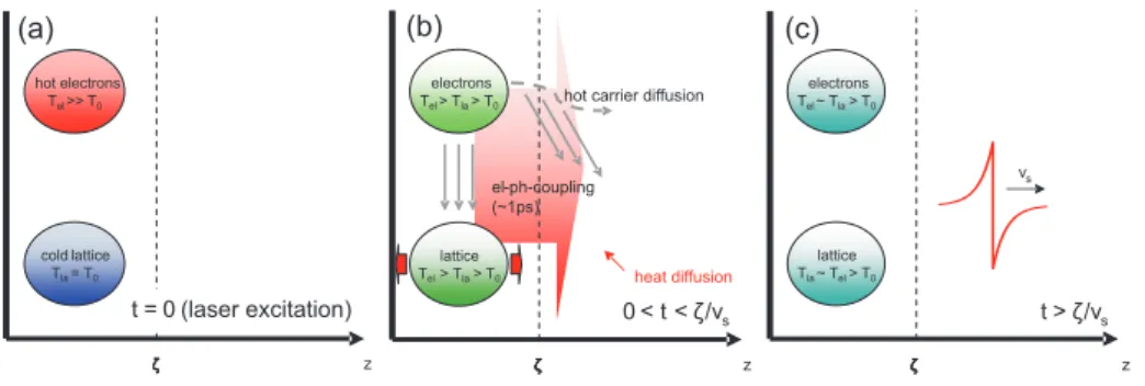
t > ζ/vs
0 < t < ζ/vs
ζζζζ lattice Tla~ Tel> T0
electrons Tel~ Tla> T0
z vs
ζζζζ lattice Tel> Tla> T0
electrons Tel> Tla> T0
z el-ph-coupling
(~1ps)
hot carrier diffusion
ζζζζ cold lattice
Tla= T0 hot electrons
Tel>> T0
z
t = 0 (laser excitation)
(a) (b) (c)
heat diffusion
Figure 2.3:
Three stages of the experimental strain wave generation process in the metal film. (a) The 150fs short excitation laser pulse heats the electron system in the surface region of the metal film within the penetration depth of light
ζaccording to Equation 2.2 to several thousand
K. (b)Energy transfer from the electron system to the lattice. Due to thermal expansion of the lattice a local thermal stress is set up in the lattice in
z-direction. The region of stress generation mightbe extended by fast heat diffusion or hot (not thermalized) electron diffusion [19] depending on the material. The time
ζ/vsindicates the escape time of the stress induced strainwave from the heated region (v
s-longitudinal sound velocity in the metal). (c) A bipolar strain pulse (red line:
Equation 2.7) has been launched into the deeper part of the metal film. A substantial part of the energy has transferred to heat, leaving the lattice and the electron system at a temperature higher than before the excitation process.
2.3 Anharmonicity: Shockwaves and Acoustic Solitons
In the previous Section 2.2 it was discussed how a propagating strain wave might be injected into a material using a metal film. The strain thereby has been considered to be the first order spatial derivative of a lattice displacement originating from co- herently excited longitudinal acoustic phonons. This section will provide a connection between the phonon concept, described in Section 2.1 and these strain waves, where the equation of motion 2.6 will be expressed in terms of energy. In this context, the harmonic approximation concerning Equation 2.1 will be extended toward higher order contributions, justifying the treatment of rather high strain amplitudes in an equation of motion beyond the harmonic approximation. In the end of this section the Korteweg-de-Vries (KdV) equation will be introduced, which describes the propagation of nonlinear dispersive strain waves and important features will be discussed.
2.3.1 Concept of Strain Energy
In order to understand the work necessary to elongate or compress a linear elastic
object consider a rod of length L like shown in Fig. 2.4 [26]. The force P necessary to
elongate the rod by ∆L thereby depends linearly on ∆L.
L
L + LD A
P P
Figure 2.4:
A rod of length
Land cross sectional area
A.The force
Prequired to elongate the rod by ∆L.
Keeping in mind that η
33= ∆L/L and σ
33= ˜ Cη
33(compare Equation 2.3) in the one dimensional case one writes for the energy
U = Z
Lη330
P d(∆L) = Z
Lη330
A C ˜
L ∆Ld(∆L) = 1
2 V Cη ˜
332= W V, (2.9) where ˜ C is an elastic constant and
W = 1
2 σ
33η
33(2.10)
denotes the work necessary to elongate a quasi one dimensional rod such that its deformation is given by η
33. The work is stored in the rod as the potential energy of deformation, which is thought to be completely recoverable by switching off P . The stress σ now can be identified as the derivative of the energy of deformation with respect to the deformation (strain), yielding the equation of motion
ρ ∂
2u
3∂t
2= ∂
∂z
∂W
∂η
33. (2.11)
Comparing the right hand side of Equation 2.11 with Equation 2.1, it is obvious that the harmonic phonon approximation is recovered in the linear elastic strain energy concept, where all changes might be expressed by the local deformation relating neigh- boring atom displacements to the undisplaced lattice. Note that the phonon dispersion relation shown in Fig. 2.2 is a result originating from the discrete character of the lat- tice, which cannot be deduced from the strain energy concept.
2.3.2 Nonlinear Elastic Expansion
Starting from the harmonic potential approximation, it is nearby to take higher order expansion coefficients into account when dealing with higher local deformation. A generalized expression of Equation 2.9 including the higher order strain energy then might be written as
W − W
0= C
ijη
ij+ 1
2 C
ijklη
ijη
kl+ 1
6 C
ijklmnη
ijη
klη
mn+ ... (2.12) with η
ij= (u
ij+ u
ji+ u
iku
kj)/2 and u
ij= ∂u
i/∂r
j(r
j, directions). The nonlinear equation of motion up to the second order of the derivatives u then reads
ρ ∂
2u
i∂t
2= ∂u
jk∂r
l(C
ijkl+ u
pqA
ijklpq) , (2.13)
where the coefficients A
ijklpqestablish the nonlinearity in the system and are given by second and third order elastic constants (see Equation 2.12)[24][25]. The physical effects arrising from Equation 2.13 will be illuminated in the next section in a simplified manner.
2.3.3 Korteweg-de-Vries Equation
In Section 2.2.1 it has been demonstrated that the induced thermal stress using a metal film and a sufficiently large area of laser excitation will lead to a localized bipolar deformation in time-space, which at most affects the z-direction i.e. the direction perpendicular to the metal film surface. This strain wave was thought to be injected into a substrate in which it might propagate over fairly long distances. In this particular case Equation 2.13 reduces to [27]
ρ ∂
2u
∂t
2=
C
2+ C
3∂u
∂z ∂
2u
∂z
2. (2.14)
For simplicity all indices have been omitted, since this equation is a scalar one. In Equation 2.14 C
2and C
3are combinations of second and third order elastic con- stants. It follows from Equation 2.14, that a high strain amplitude (∂u/∂z) wave obeys not a constant sound velocity anymore. Contrary it shows a deformation de- pendent, generalized sound velocity. Say C
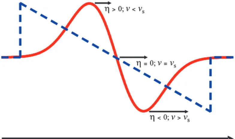
3is negative [24][27], then the compressive parts (η = ∂u/∂z < 0) of the strain wave propagate faster in time, whereas the de- compressive parts slow down, yielding a self steepening process of the leading and the trailing edge of the wave after propagation over long distances due to nonlinear elas- ticity. The self steepening process resulting in an N-shaped shockwave is visualized in Figure 2.5.
Figure 2.5:
Sketch of the spatial shape change of a high ampli- tude strain pulse after propagating through a nonlinear elastic mate- rial. (Red curve) Injected strain pulse, approximated by the deriva- tive of a gaussian function. Parts of the wave with
η <0 prop- agate faster than the longitudi- nal sound (v
s) whereas parts with
η >0 are slowed down (com- pare Equation 2.14). (Dashed blue curve) Nonlinear shockwave after long propagation distances.
v
>v
sv
<v
sv
=v
sz-direction
h
<0;h
=0;h
>0;v
>v
sv
<v
sv
=v
sz-direction
h
<0;h
=0;h
>0;Note in particular that the slope of the N-wave becomes faster after propagation at the leading and trailing edges, where it becomes slower in the center of the pulse.
The fast rise at the edges of the pulse indicate high frequency components within the
fourier spectrum of the pulse. This suggests that a dispersionless treatment of the wave is no longer valid, since high frequency acoustic phonons propagate slower than low frequency ones (see also Fig. 2.2). However, since dispersion is a result of the discrete lattice it has to be added to Equation 2.14 artificially. The highest frequencies involved are around ∼ THz. Thus the dispersion relation might be expressed as
ω
2= v
2sk
2− 2v
sγk
4+ ..., (2.15)
where v
s= (C
2/ρ)
1/2denotes the linear sound velocity and γ > 0 is the coefficient of the lowest order dispersion (v
s=4.77 km/s; γ = 0.74 in (001) GaAs [13]). The dispersive part of the motion in this case can be accounted for in Equation 2.13 by adding a term 2ρv
sγ(∂
4u/∂z
4) to the right hand side [27]. Differentiating with respect to z and replacing the displacement u by the strain η it follows:
∂
2η
∂t
2= B
12∂
2η
∂z
2+ 2B
1B
2∂
∂z
η ∂η
∂z
+ 2B
1B
3∂
4η
∂z
4+ ..., (2.16)
where
B
1= v
s, B
2= C
3/2ρv
s, B
3= γ. (2.17)
Equation 2.16 corresponds to the time derivative of the well studied Korteweg- De Vries Equation (KdV-Equation), and though contains its solutions, namely spatially unlocalized cnoidal solutions and the localized soliton solutions. Acoustic solitons in solids have been observed for the first time by H.-Y. Hao & H. J. Maris [27] and are characterized by high stability and a delicate balance concerning their nonlinear and dispersive properties. Solitons form the normal modes of the respective nonlinear system similar to the phonon modes in the linear system and therefore act as nonlinear crystal excitation with increased sound velocity [28].
Numerically calculated strain pulses with three different amplitudes before and after propagation through 114 µm GaAs material in (001) direction
2[29] are shown in Figure 2.6. The chosen incident strain amplitudes cover three distinct regimes where nonlinear elasticity and dispersion is negligible (Fig. 2.6(a)), nonlinear elasticity is dominant but dispersion is negligible (Fig. 2.6(b)) and finally both, nonlinear elasticity and dispersion are of importance during the propagation (Fig. 2.6(c)).
2
Calculated by P. J. S. van Capel -
Debye Institute, Department of Physics and Astronomy, Univer- sity of Utrecht, NetherlandsFigure 2.6:
(a) Incident (thin black line) temporal pulse shape and re- sulting (thick red line) temporal pulse shape of a strain pulse after the propagation through 114
µm(001) GaAs. Dispersion and non- linear elastic effects are negligible at the given strain amplitude re- sulting from an optical excitation density on the metal transducer of
P= 1 mJ/cm
2. (b) Same as (a) but with increased strain amplitude (P = 5.1 mJ/cm
2) and notable nonlinear elastic effects (N-wave).
(c) Same as (b) but with increased strain amplitude and notable dis- persive effects (solitons at
P= 10.2 mJ/cm
2).
-0.4 0.0 0.4
(b)
Time (ps)
Strainx10
4
(a)
-3 0 3
(c)
-30 -20 -10 0 10 20 30 40 50 60 -8
0 8
The thin black curves show the incident pulse shapes as injected from the metal film [20], which show an additional pulse feature compared to the discussion in Sec- tion 2.2 around 35 ps originating from internal acoustic reflections in the metal film.
The time separation between the first and the second feature corresponds to twice
the propagation time of the pulse through the metal film. The thick red curves show
the transformed pulses after the propagation. From Figure 2.6(a) it is obvious, that
the strain pulse shape is approximately conserved along the propagation through the
material. The pulse is almost linear, and only very weak nonlinear effects cause the
maximum and minimum to diverge slightly. In Figure 2.6(b) the situation strongly
differs. The maxima and minima of the strain pulse diverge by more than 10 ps while
the edges become fairly steep, indicating the behaviour of a nonlinear shockwave in
which the propagation speed depends on the local strain. Dispersive features are only
of minor importance at the beginning of the leading edge and the end of the trailing
edge, where a small peak and weak oscillations show up, respectively. Contrary, at
high initial strain amplitudes (Fig. 2.6(c)) the behaviour of the wave again is quali-
tatively different. The overall pulse shape has spread in time, where the trailing part
shows fast oscillations. The leading part shows three solitons, which have splitted off
during the propagation and travel with a speed considerably higher than the center
of gravity. Since real strain waves scatter on the thermal background phonons during
the propagation through a material, the above assumptions hold for low temperatures
only. To account for this a term proportional to the third order derivative of the strain
with respect to z might be added to the right hand side of Equation 2.16, yielding
the KdV-Burgers equation [24]. Since the experiments here have been performed at
low temperatures this fact is not further considered throughout this work. All of the
above mentioned three strain regimes might be realized experimentally varying the
excitation laser power on the metal film, and will lead also to various different effects
concerning the detection of the investigated acousto-optic and acousto-electro-optic
effects in Part II of this work. The basic optical properties of the studied structures
will be given in the next Chapter 3.
3 Semiconductor structures
I n Chapter 2 the principles of strain pulse generation and propagation have been reviewed. The second step is to present a basic overview concerning the optical and acoustic properties of the relevant semiconductor structures investigated in detail in this work, namely semiconductor quantum wells (QWs) and semiconductor microcav- ities (MCs). It is crucial to be aware of the mechanisms governing the optical response of these structures in order to study the interaction with the previously discussed acoustic pulses. Therefore it will be given an introduction to the optics of MCs and QWs in Section 3.1 of this chapter, as well as a description of the main principles of light-matter interaction, governing the coupled quantum well-microcavity dynamics.
Afterwards, information on the interaction mechanism between the acoustic pulses and the respective semiconductor structure will be provided in Section 3.2, differentiating displacement- and straininduced phenomena. Additional information on spectroscopic details will be given in the corresponding chapter of Part II within this work.
3.1 Optics
Since in the 1950s the transistor promised to replace the old fashioned tube tech- nology, semiconductors have evolved to be one of the main research subjects in solid state physics, where their electronic properties clearly were in the focus of interest.
The importance of the optical properties of semiconductors was recognized not much
later in the early 1960s when the possibility to fabricate semiconductor lasers was
first discovered, demonstrating the need for a fundamental knowledge concerning the
electro-optic response of semiconductors. Driven by the appearance of modelocked
titanium-sapphire lasersystems in the 1980s, semiconductor optics and electro-optics
nowadays are highly attractive for fundamental physics as well as for industrial appli-
cations, since the end of Moore’s Law’s validity seems to be close in the future. The
need for optical nanoscale devices operating at THz-frequencies has pushed the field
of semiconductor optics to the todays prominence, promising applications in informa-
tion processing and communications. The downscaling process thereby has lead to
heterostructures of various semiconductors with well defined interfaces of monoatomic
layer precision, as well as to the quantum confinement of electronic and optical states
down to zero dimensions, namely semiconductor quantum dots or nanoparticles (elec-
tronic) and photonic crystals (photonic). In the following the properties of MCs and
QWs are discussed taking over the photonic and electronic part in this work, respec-
tively.
3.1.1 Semiconductor Microcavities
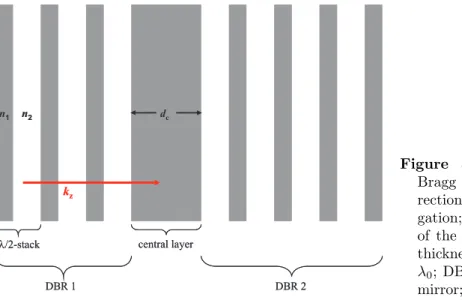
Semiconductor microcavities have been fabricated and studied in various different ways like metallic and dielectric planar cavities, pillar cavities, microsphere and microdisc cavities as well as photonic crystal cavities, all aiming at the confinement of light in certain directions[30][31][32][33][34]. Here, the investigated cavity structures are formed out of distributed Bragg reflectors (DBRs), acting as mirrors that are positioned on both sides of a central cavity layer. The DBRs in such cavities usually consist of periodic stacks of two λ
0/4-layers of different refractive indices n
1and n
2, where λ
0is given in the simplest case by the spatial extension of the central cavity layer, i.e. λ
0=n
cd
c, where d
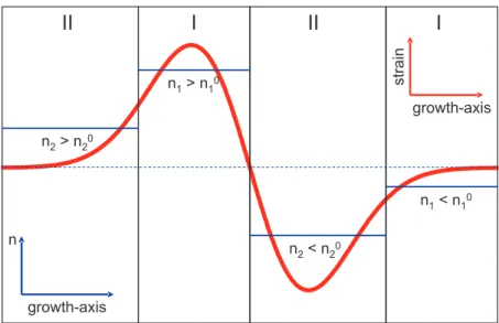
cis the thickness of the central layer. The periodic structure of the DBRs causes a photonic band gap called stop band, similar to the electronic band gaps in periodic crystal structures. Photons, propagating in the direction of the composed periodicity (say z-direction) are hindered to pass the cavity structure and are reflected efficiently. The reflected amount of light might be close to 100% depending on the photon energy, the number of stacks and the refractive index missmatch at the involved material interfaces. A sketch of such a Bragg resonator is shown in Figure 3.1.
The central layer (defect layer) gives rise to a break in the symmetrie (periodicity) of the structure. The result is a dip in the photonic stop band reflectivity allowing for spectrally well defined photons to propagate in z-direction within the structure.
n2
n1 dc
l/2-stack central layer
DBR 1 DBR 2
kz
n2
n1 dc
l/2-stack central layer
DBR 1 DBR 2
kz
Figure 3.1:
Sketch of an optical Bragg Resonator: (red arrow) Di- rection of hindered photon propa- gation;
n1and
n2refractive indices of the stack materials defining the thickness of the layers according to
λ0; DBRs forming top and bottom mirror;
dccentral layer thickness
The optical response of a stacked structure can be calculated using a transfermatrix approach matching the boundary conditions of the corresponding electric field on the interfaces according to Maxwell’s Equations [35][36]. For a TE optical wave (Trans- verse Electric), on the interface of two optical layers with refractive indices n
1, n
2, perpendicular to the layers surfaces, these boundary conditions read (transparency is assumed in the considered wavelength range)
1E
1+ E
1′= E
2+ E
′2(3.1)
1
Same for TM waves at normal incidence.
Figure 3.2:
Boundary conditions for a TE wave at the interface
i(say
i=1) of two optical layers with refractive indicesn1,n
2. For- ward and backward propagating waves are labelled with
Eiand
E′irespectively. The fields on the left side of the interface are labelled
Eiwhereas on the right side the fields are labelled
Ei+1. The dashed arrows indicate the direction of the waves magnetic field amplitude. The described model assumes the angle of inci- dence to be zero.
n
1n
2E
1E’
1E
2E’
2H
1+ H
1′= H
2+ H
′2, (3.2)
where E and H denote the electric and magnetic field of the wave, respectively, ac- cording to Figure 3.2. Replacing the magnetic field by the electric field assuming H
i= √ ǫ
iE
i= n
iE
iit is possible to combine Equations 3.1 and 3.2 in the matrix equation
2"
1 1
n
1− n
1# E
1E
1′!
=
"
1 1
n
2− n
2# E
2E
′2!
. (3.3)
The dynamical matrices D
1(n
1) and D
2(n
2) thereby describe the boundary matching of forward and backward propagating waves on the left and right side of the interface, respectively, yielding an equation relating the fields on the left and right side via a combined matrix
E
1E
1′!
= D
−11(n
1)D
2(n
2) E
2E
′2!
. (3.4)
The frequency dependence of the refractive index far off resonance has been assumed to be of minor importance in the following. Since in an extended multilayered structure the electro-magnetic wave, propagating through the layers, will change its phase, it is necessary to relate also the phases on both sides of each layer to each other, i.e.
the phases of the fields E
iand E
i. This will be accounted for using a propagation matrix P
iincluding the thicknesses d
iof the layers and only changing the phase of the respective wave. The phase change is given by
E
iE
′i!
= P (d
i, n
i) E
iE
i′!
=
"
e
iφ(di,ni)0 0 e
−iφ(di,ni)# E
iE
i′!
, (3.5)
where the phase φ
iis given by φ
i= 2πn
id
i/λ, and λ is the wavelength of the incident wave. All together the relation between forward and backward propagating waves of the first and the last (s) interface of a multilayered structure is given by
E
1(ω) E
1′(ω)
!
= D
−11(n
1)
"
sY
i=1
D
i(n
i)P
i(d
i, n
i, ω)D
i−1(n
i)
#
D
s(n
s) E
s(ω) E
′s(ω)
!
(3.6)
2
Permeability of the materials is assumed to be
µi= 1.
1.2 1.3 1.4 1.5 1.6 1.7
0.0 0.5 1.0
(c) (b) Ref lectance
Energy(eV)
(a)
44 x GaAs/AlAs layers
0.0 0.5 1.0
44 x GaAs/AlAs layers Normalized k
z
1.2 1.3 1.4 1.5 1.6 1.7
0.0 0.2 0.4 0.6 0.8 1.0
Reflectance
Energy (eV)
Figure 3.3:
Calculated optical response of DBR structures using Equation 3.6.
(a) Reflectance of a DBR with 44 GaAs/AlAs
λ0/2-layer stacks.A pro- nounced stop band is visible in the range from 1.35 eV - 1.55 eV. (b) Energy of the structure photons according to (a) in dependence of the normalized photon wavenumber
kz(real part). One corre- sponds to the brillouin zone edge orig- inating from the
λ0/2 periodicity. (c)Same as (a) but with a defect layer of thickness
ncdc=
λ0incorporated af- ter the 20th
λ0/2 stack. An additionalsharp feature occours within the stop band with reflectance smaller than one, indicating a longitudinally confined pho- ton mode. A photon with the photon mode energy might propagate within the structure in
z-direction however with de-creased speed. The speed thereby corre- sponds to the spectral width of the pho- ton mode of the microcavity (not visible here) and is a measure of ”how often”
the photon will be reflected at the mir- rors before escaping from the structure.
or
E
1(ω) E
1′(ω)
!
=
"
M
11(S, ω) M
12(S, ω) M
21(S, ω) M
22(S, ω)
# E
s(ω) E
′s(ω)
!
, (3.7)
with S, the layered structure of interest and ω, the frequency of the electromagnetic wave. In particular the reflectance of the structure is given by the squared modulus of (M
21/M
11)
2= r
c(ω) (i.e. the squared reflection coefficient of the structure) and its dispersion is given by the diagonal entries of M
ij(Fig. 3.3). The time dependence of a reflected infinitely short laser pulse is then given by the response [35]
R(t) =
1 2π
Z
res
r
c(ω)e
−iωtdω
2
, (3.8)
where ”res” denotes the spectral resonance region. An example of calculated reflectance
spectra and dispersion of DBR structures with and without defect layer is shown in
Figure 3.3. Further the matrix M
ij(S, ω) containing the optical response to an incident
wave of frequency ω can usually be expressed as M
ij(ω) if all structure parameters
are assumed to be constants. However, concerning the experiments in this work this
assumption does not hold, since a strain pulse is known to significantly alter the above
discussed parameters of the microcavity (see Chapter 3.2).
Figure 3.4:
Sketch of a QW structure. (upper part) The QW material
Bis sandwiched between the barriers of material
A. (lower part) Corresponding bandstructurein
z-direction in a type-I material composition [38].A B A
Barrier QW Barrier
CB
VB
3.1.2 Semiconductor Quantum Wells
Where in the preceding section the optical response of an optical resonator was dis- cussed, which is however a passive device, usually [37] not able to produce the photons that might be influenced by its presence, in this section the focus will be on an active medium called a semiconductor quantum well (QW). A QW is able to absorb and emit energetically well defined photons. In this structure the electronic (and hole) motion is restricted in one direction due to a composition of different band gap materials, which constitute a potential offset like sketched in Figure 3.4. This confinement gives rise to a discretisation of the quantum numbers in the respective direction and a steplike density of states compared to the square root behaviour in the bulk situation [38][39].
In particular the binding energy of the corresponding exciton (electron-hole) states [40] in a QW is increased making the resonance a very robust one with regard to the environmental temperature and applied external fields [41][42]. Further it is possible to tune the resonance energy of an exciton state by the influence of the confinement potential, tailoring the potential depth as well as its width [43]. The exciton Hamil- tonian taking into account one valence and one conduction band within the effective mass approximation is given in Equation 3.9. The discretization only acts in direction of the confinement, i.e. the direction in which the different band gap materials have been grown (say z-direction).
H = − ~
22m
e∂
2∂z
2e+ V
e(z
e) − ~
22m
h∂
2∂z
h2+ V
h(z
h) − ~
22µ
∂
2∂ρ
2x+ ∂
2∂ρ
2y− Ke
2p ρ
2+ (z
e− z
h)
2(3.9) Here m
eand m
hare the electron and hole effective masses in growth direction, respec- tively, ρ = ρ
e− ρ
his the fraction of the electron-hole distance in the plane of the QW, µ is the in-plane reduced electron-hole mass and K is a constant. The potentials V
eand V
hdescribe the confinement potential due to the band offset in z-direction usually
assumed to be steplike as sketched in Figure 3.4. It can be seen from Equation 3.9 that
0 E
gap
E gap
LH HH
Energy
wavenumber k x,y CB
QW
Figure 3.5:
Sketch of a two dimensional (zinc blende) QW bandstructure (three bands). The two hole bands (dashed line: HH; dotted line: LH) lift their degeneracy in contrast to the bulk case for
kx,y= 0 due to the
kz-quantization with different effective masses
m∗z,HHand
m∗z,LHand the band gap
Egapis effectively increased (E
gapQW). In particular it is
m∗z,HH > m∗z,LHperpendicular to the QW plane, where
m∗x,y,HH< m∗x,y,LHin the plane of the QW.
The two valence bands anticross in the full Lut- tinger description [44].
the exciton solutions might be separable into z- and ρ-direction components depending on which direction has the largest impact on the coulomb term in the hamiltonian.
However, the excitons get quantized in z-direction if the potential width of V
e,h(z
e,h) is
sufficiently small ((z
e− z
h)
2<< ρ
2), which means that the dispersion of the electron
and hole band, taken to be ∼ k
2in the bulk material turns into a constant offset in
z-direction proportional to the inverse electron and hole effective masses [38]. The
two dimensional bandstructure of a QW (zinc blende), including one conduction band
(CB) and two (heavy hole HH, light hole LH) valence bands, is sketched in Figure 3.5
according to the quantized Luttinger Hamiltonian [44]. Later on in this work k
x,ywill
be assumed to be close to zero in all cases. This leads to two distict exciton resonances
in the optical spectrum, due to the coulomb coupling of the conduction band to the
heavy hole as well as to the light hole bands (see Figure 3.6). A lift of the degeneracy
might also be caused by stress applied to the structure. This may leads to a shift of
the bands due to the materials deformation potentials, yielding a change in exciton
resonance energy. A further discussion of this effect will be presented in Chapter 3.2.
Figure 3.6:
Measured reflectance of a ZnSe QW em- bedded between ZnMgSSe barriers [29]. Two ex- citon resonances are seen, namely the HH-exciton and the LH-exciton at lower and higher energies respectively.
2.78 2.79 2.80 2.81 2.82 2.83 2.84 2.85 0.7
0.8 0.9 1.0 1.1 1.2 1.3
LH-exciton
Reflectance
Energy (eV) HH-exciton
The reflectance spectrum shown in Figure 3.6 differs from the simple shape of QW reflectance as given in references [38] and [35], which can be explained by additional interferences due to the QW top barrier layer thickness [45]. The spectral shape of the excitons (Fig. 3.6) can be written as
r
QWi(ω) = 1 + A
i~ (ω − ω
i)
Γ
2i+ ~
2(ω − ω
i)
2, (3.10) where ~ ω
iis the respective resonance energy (i = LH, HH), Γ
idenotes the resonances widths as seen from the measured spectrum, and the A
iare scaling constants.
3.1.3 Principles of Light-Matter Interaction
In this section a basic idea of light-matter interaction will be given, bringing together the previously discussed MC and QW structures. Consider a QW inside a MC at the antinode position of the confined light field (center of the defect layer). Matching the resonance energy of the confined exciton (say HH-exciton) to the confined cavity mode, it is possible to strongly enhance the light matter coupling, which is - without a cavity - limited by the QW’s spatial extension. In particular it is possible to reach the strong coupling regime using a single QW in a planar MC structure as demonstrated by C.
Weisbuch et al. [46].
The regimes of light-matter interaction can be distinguished by the relation of cou-
pling parameters within the considered system. Where the exciton might couple to the
environment by photons, leaving the QW or via interaction with phonons, the cavity
will release photons with a coupling strength to the environment corresponding to its
capability to confine photons as described in Chapter 3.1.1. However if these mecha-
nisms are predominant in comparison to the exciton-cavity coupling, one speaks about
the weak coupling regime, where the cavity mode principally acts as a filter function
for the exciton. Nevertheless the radiative properties of the exciton will be altered due
to the cavity’s influence on the optical density of states, which may culminate in the
purcell effect in completely confined photonic cavities [47]. If on the other hand a pho-
ton at resonance energy has the possibility to interact with the QW-exciton sufficiently
often due to a high internal reflection propability at the cavity walls, and likewise the
photon absorption propability is efficient, the photon may be absorbed and reemitted several times before leaving the cavity. The state of such a system is no longer a pure photonic or excitonic state. Rather, the mixture of both states is called a polariton state i.e. a strongly coupled light-matter state, that manifests in an upper polariton and a lower polariton branch, in the following refered as upper (UP) and lower (LP) polariton. The energies of these lower and upper polariton branches are shifted with respect to the uncoupled cavity and exciton resonances towards lower (LP) and higher (UP) energies.
Here the main attention will be on the polariton energies and their photonic and exci- tonic character. To this extend the main results from a (semi) classical treatment will be introduced.
From the classical point of view it is apparent that the modes of two coupled ideal oscillators will not exhibit the same energies, irrespective of how the parameters of the system are changed. This phenomenon is known as the normal mode anticrossing, where the normal modes are assumed to be the new eigenstates of the coupled sys- tem. Assuming the exciton and the photon state in the cavity to be oscillators with the complex frequencies ω
l− iγ
l(l = x and l = c for the exciton and photon state respectively), one writes the coupled mode equation as [35][38]
(ω
x− iγ
x− ω)(ω
c− iγ
c− ω) = V
2. (3.11) In Equation 3.11 the imaginary parts γ
lof the uncoupled exciton polarisation and photon eigenfrequencies introduce the coupling to the environment of each mode (ex- citon nonradiative coupling). The coupling parameter V describes the exciton photon interaction strength. Solving Equation 3.11 with respect to ω yields two polariton frequencies
ω
UP,LP= ω
x+ ω
c2 − i
2 (γ
x+ γ
c)
±
"
ω
x− ω
c2
2+ V
2−
γ
x− γ
c2
2+ i
2 (ω
x− ω
c)(γ
c− γ
x)
#
12(3.12)
as long as the squareroot term remains a real term. The polariton energies from Equation 3.12 might be written as ~ ω
UP,LP= E
UP,LP(E
x, E
c, γ
x, γ
c, V ). Defining the detuning
∆
d= E
x− E
c(3.13)
one may write
E
UP(∆
d= 0) − E
LP(∆
d= 0) = 2 ~ Ω
R, (3.14) where Ω
Ris the so called Rabi-Frequency of the system, defining the minimum nor- mal mode splitting as well as the frequency, with which the probability to find one of the polariton branches in a certain superposition state has swapped to the other branch and back. 2Ω
Rconstitutes the beating frequency of both polariton branches.
The polariton branches consist of a photonic and an excitonic part with periodically
oscillating propability amplitudes in time. The wavefunction of the overall polariton state reads [48]
| Ψ i = | UP i + | LP i = (a
1(∆
d) | C i + a
2(∆
d) | X i ) + (a
1(∆
d) | X i − a
2(∆
d) | C i ) (3.15) with | X i , | C i beeing the uncoupled exciton and cavity (photon) state vectors, and the Hopfield Coefficients [49] a
1(∆
d) and a
2(∆
d), which constitute the detuning dependent UP excitonic and photonic character, respectively (vice versa for the LP). Explicitly, the Hopfield Coefficient in the considered system read
a
1= V
p 2∆
1(∆
1+ ∆
2) , a
2=
r ∆
1+ ∆
22∆
2,
∆
1= (ω
x− ω
c)/2, ∆
2= q
∆
21+ V
2.
(3.16)
Figure 3.7(a) shows the dependence of the polariton energies on the underlying exciton energy at fixed E
c. At resonance, i.e. ∆
d= 0, the two branches anticross with a minimum energy distance of 2 ~ Ω
R. In contrast at increasing large values of ∆
d(far from resonance) the two polariton energies asymptotically approach the corresponding uncoupled state energies and likewise adopt the corresponding photonic (excitonic) content (Fig. 3.7(b)). At very large detunings Equations 3.12, 3.15 and 3.16 recover completely the underlying uncoupled exciton and cavity photon states.
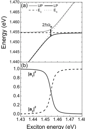
Figure 3.7:
Calculated polariton properties ac- cording to Equations 3.12 and 3.16. The pa- rameter have been chosen to be in agreement with the sample from Chapter 9 at zero angle of incidence. (a) UP and LP polariton ener- gies in dependence on the underlying exciton energy
Ex(dotted line). The cavity photon energy
Ec(dashed line) is held constant. The polariton energies anticross at resonance i.e.
Ex
=
Ecwith a splitting according to Equa- tion 3.14. (b) Same dependence as in (a) but for the Hopfield Coefficients
|a1|2and
|a2|2fol- lowing Equation 3.16.
1.43 1.44 1.45 1.46 1.47 1.48 0.0
0.2 0.4 0.6 0.8 1.0
|a 2
| 2
Exciton energy (eV)
|a 1
| 2 1.440
1.445 1.450 1.455 1.460 1.465 1.470
(b)
UP LP
E C
E X
Energy(eV)
2 R (a)
![Figure 3.6: Measured reflectance of a ZnSe QW em- em-bedded between ZnMgSSe barriers [29]](https://thumb-eu.123doks.com/thumbv2/1library_info/3647529.1503107/29.892.455.743.102.323/figure-measured-reflectance-znse-qw-bedded-znmgsse-barriers.webp)