Hall field-induced resistance oscillations in a tunable-density GaAs quantum well
M. A. Zudov,1I. A. Dmitriev,2,3,4B. Friess,3Q. Shi,1V. Umansky,5K. von Klitzing,3and J. Smet3
1School of Physics and Astronomy, University of Minnesota, Minneapolis, Minnesota 55455, USA
2Department of Physics, University of Regensburg, D-93040 Regensburg, Germany
3Max Planck Institute for Solid State Research, Heisenbergstrasse 1, D-70569 Stuttgart, Germany
4Ioffe Physical Technical Institute, 194021 St. Petersburg, Russia
5Braun Centre for Semiconductor Research, Department of Condensed Matter Physics, Weizmann Institute of Science, Rehovot 76100, Israel
(Received 7 August 2017; published 11 September 2017)
We report on Hall field-induced resistance oscillations (HIROs) in a 60-nm-wide GaAs/AlGaAs quantum well with anin situgrown back gate, which allows tuning the carrier densityn. At lown, when all electrons are confined to the lowest subband (SB1), the HIRO frequency, proportional to the product of the cyclotron diameter and the Hall field, scales withn−1/2 as expected. Remarkably, the population of the second subband (SB2) significantly enhances the HIROs, whereas their frequency now scales asn−1. We demonstrate that in this two-subband regime HIROs still originate solely from backscattering of SB1 electrons. The unusual density dependence occurs because the population of SB2 steadily increases, whereas that of SB1 remains essentially unchanged. The enhancement of the HIROs manifests an unexpected steplike increase in the quantum lifetime of SB1 electrons, which reaches a record value of 52 ps in the two-subband regime.
DOI:10.1103/PhysRevB.96.121301
Continuous developments [1–8] in the molecular beam epitaxy and heterostructure design of two-dimensional elec- tron systems (2DES) have led to discoveries of a plethora of novel phenomena, especially in the field of low-temperature magnetotransport. Apart from the extremely rich quantum Hall physics in strong magnetic fields [9,10], high-mobility 2DES display many prominent transport phenomena in low fields.
Two salient examples of such phenomena are microwave- induced resistance oscillations (MIROs) [11–16] and Hall field-induced resistance oscillations (HIROs) [17–26] which emerge when a 2DES is driven by microwave radiation and direct current, respectively.
HIROs emerge due to elastic electron transitions between Landau levels, tilted by the Hall field, as a result of backscat- tering off short-range impurities [17,27,28]. The probability of these transitions is maximized each time the Hall voltage drop across the cyclotron diameter matches an integer multiple of the cyclotron energy. As a result, the differential resistivity acquires a 1/B-periodic correctionδrwhich can be described by [27]
δr/ρ0≈(16τ /π τπ)λ2cos(2π B1/B), (1) whereρ0 =m/e2nτ is the resistivity at zero-magnetic-field B, m≈0.07m0is the effective mass,nis the electron density, λ=exp(−π/ωcτq) is the Dingle factor,ωc=eB/m is the cyclotron frequency, andτ,τπ,τqare transport, backscattering, and quantum lifetimes, respectively [29]. The HIRO frequency (inverse period)B1is given by
B1
B ≡eE(2Rc)
¯
hωc ⇒B1=
8π
n m
e2j, (2) whereE=Bj/neis the Hall field andRc=h¯√
2π n/eB is the cyclotron radius.
It is well known that, in systems with several populated subbands, MIROs and HIROs often mix with magneto-inter- subband oscillations (MISOs) [30–36]. However, it is also
important to examine how MIROs and HIROs are affected by the population of the second subband in the absence of such mixing. For example, capacitance measurements in a wide quantum well provided direct evidence of microwave- induced nonequilibrium redistribution of electrons between two subbands but no significant change in the MIROs upon a second subband population [37]. However, unlike MIROs, whose frequencymω/e(ωbeing the microwave frequency) is density independent, the HIRO frequency in the single- subband regime B1 scales as n−1/2, which stems from the product of Rc∝√
n and E∝n−1 [see Eq. (2)]. It is thus interesting to explore how HIROs evolve with the populations of the lowest subband (SB1) and the first excited subband (SB2) and to detect HIRO contributions from each subband, which should provide access to their individual scattering rates.
In this Rapid Communication we report on Hall field- induced resistance oscillations in a density-tunable wide quantum well in which electrons form two parallel layers when the second subband becomes populated [37–39]. Remarkably, in the two-subband regime, we still observe only one set of HIROs but find that their frequency scales as 1/n, seemingly in contradiction with Eq. (2). As demonstrated below, this finding indicates that HIROs still originate from backscattering of SB1 electrons only (whose density remains approximately constant in the two-subband regime), whereas the Hall field Eis produced by electrons in both subbands. We further find that HIROs become markedly enhanced in the two-subband regime. This enhancement was not anticipated but can be linked to an abrupt increase in the quantum scattering time of SB1 electrons. One possible reason for such an increase is an additional screening of the long-range scattering potential by SB2 electrons. The absence of HIROs from SB2 electrons can be explained by their considerably shorter quantum scattering time. This conclusion is supported by a complementary analysis of MISOs.
Our lithographically defined Hall bar (width w= 0.4 mm) sample was fabricated [40] from a GaAs/AlGaAs
Ρ
FIG. 1. Differential resistivityr, normalized toρ0, vsBatI= 50μA and at gate voltages fromVg= −0.2 V (top) to 1.2 V (bottom), in steps of 0.1 V. The traces are vertically offset for clarity by 0.2 (bottom to top). Numbers next to the bottom trace mark HIRO maxima nearB1/B=1, 2, and 3.
heterostructure containing a 60 nm-wide quantum well. The structure was modulation doped on the top side using a short-period superlattice positioned 66 nm away from the quantum well. An additional in situ grown doped quantum well, located 800 nm below the main quantum well, served as a gate to tune the carrier density [38,41]. At zero gate voltage, the electron density and the mobility weren≈1.1×1011cm−2 andμ≈5.8×106cm2V−1s−1, respectively. The differential longitudinal resistivity r=dV /dI, where V is the voltage drop between contacts positioned 1.26 mm apart along the Hall bar, and the Hall resistivity were measured while sweeping B using a standard four-terminal lock-in technique (0.5μA excitation) in a3He cryostat at a base temperature of 0.3 K.
In Fig.1we present the differential resistivity normalized to the zero-field resistivity as a function of the magnetic field measured in the presence of a direct currentI =50μA. The gate voltage serves as a discrete parameter and is varied from Vg = −0.2 V (top, lowest density) to+1.2 V (bottom, highest density) in steps of 0.1 V. Traces are vertically offset by 0.2 (bottom to top). All traces show HIROs with maxima (marked by 1, 2, and 3 at the bottom trace) moving towards lowerBwith increasing Vg (density). Concurrently, the HIRO amplitude gradually increases at low Vg but then suddenly jumps at Vg ≈0.3 V (cf. thick line). Beyond this gate voltage, HIROs persist down to very lowB <0.01 T. As shown below, this abrupt enhancement of HIROs coincides with the onset of SB2 population, which is accompanied by a significant increase in the quantum lifetime of SB1 electrons.
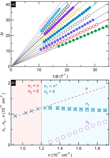
To obtain the electron density for the individual subbands n1andn2, we exploit the period of MISOs visible in Fig.1as
(a)
(b)
FIG. 2. (a) MISO orderNvs 1/BforVgfrom+1.2 V (bottom) to+0.3 V (top), in steps of 0.1 V. Lines are fits to Eq. (4). (b)n1
(squares) andn2 (circles), obtained from Eq. (5), andn1 (crosses), obtained from Eq. (2) (n < n) and Eq. (6) (n > n), as a function of n. The dashed line representsn=n1+n2.
fast oscillations. MISOs are described by [30,42–44]
δρ/ρ0=(2τ/τ12)λ1λ2cos(2π /hω¯ c), (3) where is the inter-subband separation, τ12 is the inter- subband transport scattering time, andλ1(λ2) is the Dingle factor of SB1 (SB2) electrons. TheNth MISO maximum thus occurs when
¯
hωc = h eB
δn
2 =N, (4)
whereδn≡n1−n2.
In Fig.2(a)we showN as a function of 1/Bfor different Vg from 1.2 V (bottom) to 0.3 V (top) in steps of 0.1 V. As prescribed by Eq. (4), all data sets exhibit linear dependencies.
From the slope of these dependencies we obtainδnand the subband populations as
n1,2= n±δn
2 , (5)
where +(−) corresponds ton1(n2) and the total densityn is found from the Hall resistivityρH =B/ne. The obtained values ofn1(squares) andn2(circles) are presented in Fig.2(b)
Μ Μ
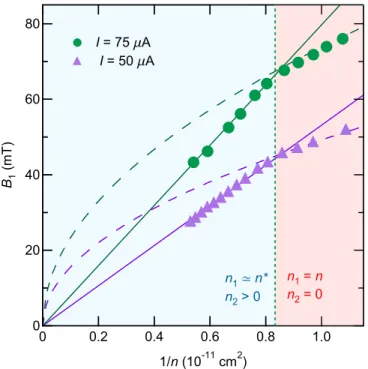
FIG. 3. Magnetic-fieldB1 vs 1/nforI=75μA (circles) and I=50 (triangles). The vertical dotted line marks the onset of SB2 population. The solid and dashed lines are calculated using Eq. (6) withn1=nand Eq. (2), respectively.
as a function ofn. Forn > n≈1.2×1011 cm−2, n1 shows little change, remaining close to n [45], i.e., the change in (dashed line) occurs due to increasing n2 only. These findings conform with earlier studies of such heterostructures [38,39,46]. In particular, calculations [38] revealed a strong spatial separation of the wave functions of SB1 and SB2 electrons. At high Vg, SB1 electrons are located near the front interface of the quantum well (closer to the donor layer), whereas SB2 electrons reside near the back interface (closer to the gate). This fact explains whyn2 increases at the same rate asnwhilen1remains essentially unchanged.
We next note that, even when SB2 is populated, HIROs remain periodic in 1/B. This observation alone suggests that HIROs still originate predominantly from transport within a single subband. In Fig.3 we presentB1, extracted from the data obtained atI =75μA (circles) andI =50 (triangles), as a function of 1/n. Both dependencies reveal two distinct regimes separated by a kink at n≈n. For the single- subband case, n < n, one finds B1∝n−1/2, in agreement with Eq. (2) (dashed lines). At n > n, both dependencies change to B1∝1/n (cf. solid lines), reflecting that HIROs stem from backscattering of SB1 electrons only. Indeed, whereas the Hall field is determined by the total density n, the cyclotron diameter of electrons in SB1 is controlled byn1. As a result, the HIRO frequency in this regime needs to be modified as
B1=
√8π n1
n m
e2j. (6)
Sincen1≈const atn > n, one readily concludes thatB1∝ 1/n. We can confirm the above picture by estimatingn1from the HIRO frequency employing Eq. (2) atn < nand Eq. (6)
Τ
Ρ
(a)
(b)
FIG. 4. (a) Differential resistivityr, normalized toρ0vsBmea- sured atI=50μA and at a gate voltageVg=1.2 V (n=1.88× 1011cm−2). The thick lines mark HIROs’ maxima corresponding to B/B1=1–3 [47]. The thin lines mark MISOs’ maxima. (b) Reduced HIROs’ amplitudeA=(π/16)(|δrmax|/r0) [see Eq. (1)] as a function of 1/Bon a log-linear scale forn=1.37×1011cm−2(filled circles) andn=1.88×1011cm−2 (open circles). The fit (straight line) to (τ/τπ) exp(−2π/ωcτq1) yieldsτq1≈52 ps andτ/τπ ≈0.36.
atn > n. The obtained values ofn1 [marked by crosses in Fig.2(b)] are in excellent agreement with n at n < n and withn1obtained from Eq. (5) atn > n.
Next, we take a closer look at HIROs in the two-subband regime. A representative trace is shown in Fig.4(a)displaying r/ρ0vsBmeasured atI =50μA andn=1.88×1011cm−2. The positions of the thick vertical lines, which pass through the HIRO maxima, are calculated using Eq. (6). As noticed earlier, HIROs persist down to a very lowB≈0.0075 T, suggesting a long quantum lifetime of SB1 electronsτq1. To access its value, we construct a Dingle plot which is shown in Fig.4(b). The reduced HIRO amplitudeA=(π/16)(|δrmax|/r0) [see Eq. (1)]
is plotted as a function of 1/B on a log-linear scale forn= 1.37×1011 cm−2 (filled circles) and n=1.88×1011 cm−2 (open circles). Remarkably, both data sets collapse on the same line indicating that, once SB2 is populated, a further increase inn2 has a negligible effect onA. The amplitudeA exhibits the expected exponential dependence, and the fit (solid line) yieldsτq1 ≈52 ps. This value translates to a quantum
ΜΜ
Μ Μ
FIG. 5. Mobility μ (squares) and quantum mobility of SB1 electronsμq1(circles) [50] as a function ofn.
mobility ofμq1≡eτq1/m≈1.3×106cm2V−1s−1, which, to our knowledge, is the largest value ever reported in any system [48,49]. The intercept of the fit with 1/B=0 gives τ/τπ ≈0.36, implying that backscattering of SB1 electrons provides an essential fraction of the total transport scattering rate. The quantum mobilityμq1(n) is shown in Fig.5together with the transport mobilityμ(n) measured atB =0.
The overlapping Dingle plots in Fig.4(b)indicate that both τπ andτq do not vary in the two-subband regime. It is thus reasonable to expect that the transport mobility μ1 of SB1 electrons also stays constant atn > n. This assumption en- ables us to estimate mobility of the second subbandμ2. Indeed, using the relations μn=μ1n1+μ2n2 [51], n1≈n, and n2≈n−n, we find μ2(n)≈[nμ(n)−nμ(n)]/(n−n), where μ1 ≈μ(n)8×106cm2V−1s−1. This procedure yieldsμ2≈7×106cm2V−1s−1 atn2 =0.75×1011 cm−2, i.e.,μ2≈μ1even thoughn2< n1.
With the knowledge of τq1, we also can estimate the quantum lifetime of SB2 electrons τq2 by employ- ing the fact that the MISO amplitude decays as λ1λ2= exp(−π/ωcτq1) exp(−π/ωcτq2), see Eq. (3). The corre- sponding Dingle analysis yields τq2≈14 ps (μq2≈0.35× 106cm2V−1s−1) at n2=0.75×1011cm−2 [52]. The low value ofτq2readily explains why no HIROs from SB2 electrons [that would decay as exp(−2π/ωcτq2)exp(−2π/ωcτq1)]
are detected. Indeed, HIROs are barely visible at the lowest n=n1(cf. top trace in Fig.1), even thoughμq1is twice as high.
We next discuss possible reasons why μq2≈0.3μq1 (at the highestn), which is rather surprising in view ofμ2≈μ1. Although at the highestn, n1is 50% higher thann2, this fact alone cannot account for the observed difference betweenμq2 andμq1. In modulation-doped structures, a largeμi/μq,iratio reflects dominance of small-angle scattering originating from donors separated by a spacer of thickness d1 (d1=66 nm in our sample). Based on our estimates above, we obtain, at the highestn, μ1/μq1≈6 andμ2/μq2≈20, which indicates that SB2 electrons experience a much stronger small-angle scattering. However, one can expect just the opposite relation
since: (i) SB2 electrons are further away from the donor layer, and (ii) SB1 electrons should effectively screen the random potential from this layer. For the same reason, a strong (about 50%) enhancement ofτq1in the two-subband regime [53,54], shown by the circles in Fig.5, is also puzzling as it cannot be attributed to an additional screening of the donor random potential by SB2 electrons.
To explain our findings, one apparently needs to consider another kind of distant scatterers, located closer to the back side of the quantum well. One possible source of such scatterers is the doped GaAs quantum well (serving as a back gate), located at a distance ofd2=800 nm. Since the gate is much farther away than the donor layer (d1/d2∼0.1), it has a negligible impact on mobility. However, it can still reduce the quan- tum mobility which is dominated by small-angle scattering [55]; with a random charge density of n2=1×1011cm−2, it would limit the quantum mobility of SB2 electrons to μq2≈(4ed2/h)/¯ √
2π n2≈0.6×106cm2V−1s−1 [44]. This estimate is not unreasonable [56], considering that other scattering sources further diminish μq2. Almost complete screening of the gate random potential by SB2 electrons should then lead to an enhancement ofμq1 observed at the onset of the population of the second subband. Similarly, SB2 electrons should partially screen the long-range component of the potential created by background impurities leading to further enhancement ofμq1 in the two-subband regime.
The above discussion demonstrates that combined analysis of the various magneto-oscillations in multi-subband het- erostructures provides rich information on the characteristics of the disorder potential, which may help to improve our understanding and allow for technologically controlling the role of particular scattering sources.
To summarize, we have studied nonlinear magnetotransport in a 60-nm-wide GaAs/AlGaAs quantum well equipped with an in situ grown back gate for tuning the carrier density n. An analysis of HIRO and MISO frequencies indicates that the occupation of the second subband is triggered at n=n≈1.2×1011cm−2. At (n < n)n > n, we find that the HIRO frequency increases asn−1/2(n−1), indicating that the observed HIROs originate from backscattering of SB1 electrons at all densities studied. Remarkably, when SB2 becomes populated, HIROs suddenly become much more pronounced. Our analysis shows that this HIRO enhancement is due to an abrupt increase in the quantum lifetime of SB1 electrons. It approaches a record value of 52 ps in the two-subband regime of transport. The enhancement likely originates from additional screening of the disorder potential by SB2 electrons.
We thank J. Falson for assistance with the experimental setup and M. Borisov for performing the Dingle analysis of the MISOs. The work at the University of Minnesota was funded by the US Department of Energy, Office of Science, Basic Energy Sciences, under Award No. ER 46640-SC0002567.
Q.S. acknowledges support from a University of Minnesota Doctoral Dissertation Fellowship. I.A.D. acknowledges finan- cial support from the German Research Foundation (DFG Grant No. DM1/4-1). V.U. and J.S. acknowledge financial support from the GIF.
[1] L. Pfeiffer, K. W. West, H. L. Stormer, and K. W. Baldwin,Appl.
Phys. Lett.55,1888(1989).
[2] V. Umansky, R. de Picciotto, and M. Heiblum,Appl. Phys. Lett.
71,683(1997).
[3] L. Pfeiffer and K. W. West,Physica E20,57(2003).
[4] V. Umansky, M. Heiblum, Y. Levinson, J. Smet, J. Nübler, and M. Dolev,J. Cryst. Growth311,1658(2009).
[5] V. Umansky and M. Heiblum, inMolecular Beam Epitaxy: From Research to Mass Production, edited by M. Henini (Elsevier, Waltham, MA, 2013), pp. 121–137.
[6] M. J. Manfra, Annu. Rev. Condens. Matter Phys. 5, 347 (2014).
[7] J. D. Watson, G. A. Csáthy, and M. J. Manfra,Phys. Rev. Appl.
3,064004(2015).
[8] G. C. Gardner, S. Fallahi, J. D. Watson, and M. J. Manfra, J. Cryst. Growth441,71(2016).
[9] K. von Klitzing, G. Dorda, and M. Pepper,Phys. Rev. Lett.45, 494(1980).
[10] D. C. Tsui, H. L. Stormer, and A. C. Gossard,Phys. Rev. Lett.
48,1559(1982).
[11] M. A. Zudov, I. V. Ponomarev, A. L. Efros, R. R. Du, J. A.
Simmons, and J. L. Reno,Phys. Rev. Lett.86,3614(2001).
[12] P. D. Ye, L. W. Engel, D. C. Tsui, J. A. Simmons, J. R. Wendt, G. A. Vawter, and J. L. Reno, Appl. Phys. Lett. 79, 2193 (2001).
[13] R. G. Mani, J. H. Smet, K. von Klitzing, V. Narayanamurti, W. B. Johnson, and V. Umansky,Nature (London) 420, 646 (2002).
[14] M. A. Zudov, R. R. Du, L. N. Pfeiffer, and K. W. West,Phys.
Rev. Lett.90,046807(2003).
[15] M. A. Zudov, O. A. Mironov, Q. A. Ebner, P. D. Martin, Q. Shi, and D. R. Leadley,Phys. Rev. B89,125401(2014).
[16] D. F. Kärcher, A. V. Shchepetilnikov, Y. A. Nefyodov, J. Falson, I. A. Dmitriev, Y. Kozuka, D. Maryenko, A. Tsukazaki, S. I.
Dorozhkin, I. V. Kukushkin et al.,Phys. Rev. B 93, 041410 (2016).
[17] C. L. Yang, J. Zhang, R. R. Du, J. A. Simmons, and J. L. Reno, Phys. Rev. Lett.89,076801(2002).
[18] A. A. Bykov, J.-q. Zhang, S. Vitkalov, A. K. Kalagin, and A. K.
Bakarov,Phys. Rev. B72,245307(2005).
[19] W. Zhang, H.-S. Chiang, M. A. Zudov, L. N. Pfeiffer, and K. W.
West,Phys. Rev. B75,041304(R)(2007).
[20] A. A. Bykov, J.-Q. Zhang, S. Vitkalov, A. K. Kalagin, and A. K. Bakarov,Phys. Rev. Lett.99,116801(2007).
[21] W. Zhang, M. A. Zudov, L. N. Pfeiffer, and K. W. West,Phys.
Rev. Lett.100,036805(2008).
[22] A. T. Hatke, M. A. Zudov, L. N. Pfeiffer, and K. W. West,Phys.
Rev. B79,161308(R)(2009).
[23] A. T. Hatke, H.-S. Chiang, M. A. Zudov, L. N. Pfeiffer, and K. W. West,Phys. Rev. B82,041304(R)(2010).
[24] A. T. Hatke, M. A. Zudov, L. N. Pfeiffer, and K. W. West,Phys.
Rev. B83,081301(R)(2011).
[25] Q. Shi, Q. A. Ebner, and M. A. Zudov, Phys. Rev. B 90, 161301(R)(2014).
[26] Q. Shi, M. A. Zudov, J. Falson, Y. Kozuka, A. Tsukazaki, M. Kawasaki, K. von Klitzing, and J. Smet,Phys. Rev. B95, 041411(R)(2017).
[27] M. G. Vavilov, I. L. Aleiner, and L. I. Glazman,Phys. Rev. B 76,115331(2007).
[28] X. L. Lei,Appl. Phys. Lett.90,132119(2007).
[29] The rate of scattering on angleθ can be expressed in terms of angular harmonics asτθ−1=
τn−1einθ. In this notation,τq−1= τ0−1, τ−1=τ0−1−τ1−1, andτπ−1=
(−1)nτn−1. [30] O. E. Raichev,Phys. Rev. B78,125304(2008).
[31] S. Wiedmann, G. M. Gusev, O. E. Raichev, T. E. Lamas, A. K.
Bakarov, and J. C. Portal,Phys. Rev. B78,121301(2008).
[32] N. C. Mamani, G. M. Gusev, O. E. Raichev, T. E. Lamas, and A. K. Bakarov,Phys. Rev. B80,075308(2009).
[33] S. Wiedmann, G. M. Gusev, O. E. Raichev, A. K. Bakarov, and J. C. Portal,Phys. Rev. B81,085311(2010).
[34] S. Wiedmann, G. M. Gusev, O. E. Raichev, A. K. Bakarov, and J. C. Portal,Phys. Rev. Lett.105,026804(2010).
[35] S. Wiedmann, G. M. Gusev, O. E. Raichev, A. K. Bakarov, and J. C. Portal,Phys. Rev. B84,165303(2011).
[36] G. M. Gusev, S. Wiedmann, O. E. Raichev, A. K. Bakarov, and J. C. Portal,Phys. Rev. B83,041306(2011).
[37] S. I. Dorozhkin, A. A. Kapustin, V. Umansky, K. von Klitzing, and J. H. Smet,Phys. Rev. Lett.117,176801(2016).
[38] J. Nuebler, B. Friess, V. Umansky, B. Rosenow, M. Heiblum, K.
von Klitzing, and J. Smet,Phys. Rev. Lett.108,046804(2012).
[39] S. I. Dorozhkin,JETP Lett.103,513(2016).
[40] Independent contacts to the active layer and the back gate were fabricated using a two-step etching technique, see, e.g., Ref. [7].
[41] See Ref. [38] for more information about spectral and transport properties of this type of heterostructure.
[42] M. E. Raikh and T. V. Shahbazyan,Phys. Rev. B49,5531(1994).
[43] N. S. Averkiev, L. E. Golub, S. A. Tarasenko, and M. Willander, J. Phys.: Condens. Matter13,2517(2001).
[44] I. A. Dmitriev, A. D. Mirlin, D. G. Polyakov, and M. A. Zudov, Rev. Mod. Phys.84,1709(2012).
[45] In fact,n1shows a slightdecreaseat highern.
[46] K. Muraki, N. Kumada, T. Saku, and Y. Hirayama,Jpn. J. Appl.
Phys.39,2444(2000).
[47] The position of the first maximum was obtained using a more accurate expression [26,27] obtained from Eq. (1) by replacing cos 2π jwith (π/2)[J12(π j)−2π jJ0(π j)J1(π j)].
[48] A comparableτqvalue of 46 ps recently was found from Dingle analysis of MIROs in a 30-nm GaAs/AlGaAs quantum well with ne≈3.2×1011cm−2andμ≈3.1×107cm2V−1s−1[49].
[49] Q. Shi, S. A. Studenikin, M. A. Zudov, K. W. Baldwin, L. N.
Pfeiffer, and K. W. West,Phys. Rev. B93,121305(R)(2016).
[50]μq1was obtained from the fit of ther(B) data with the theoretical expression shown in Ref. [47].
[51] Althoughμ1,2includes both intra- and inter-subband scattering, the latter is relatively weak [52].
[52] The intercept of the MISO Dingle plot yieldsτ/τ12<0.1, sug- gesting the relative unimportance of inter-subband scattering.
[53] A phenomenologically similar increase previously was observed in the lifetime describing damping of the commensurability oscillations [54]. It was attributed to the doubling of the screening wave vector due to the doubling of the total 2DES density of states at the onset of SB2 population.
[54] J. P. Lu and M. Shayegan,Phys. Rev. B58,1138(1998).
[55] Q. Qian, J. Nakamura, S. Fallahi, G. C. Gardner, J. D. Watson, S. Lüscher, J. A. Folk, G. A. Csáthy, and M. J. Manfra,Phys.
Rev. B96,035309(2017).
[56] Application of the same procedure to the donor layer would result in underestimatedμq1, likely because it ignores screening of ionized donors byXelectrons in AlAs layers surrounding the GaAs doping well.
![FIG. 5. Mobility μ (squares) and quantum mobility of SB1 electrons μ q1 (circles) [50] as a function of n.](https://thumb-eu.123doks.com/thumbv2/1library_info/3944709.1534056/4.911.79.444.104.365/fig-mobility-squares-quantum-mobility-electrons-circles-function.webp)
