Tuning Methods for Semiconductor Spin Qubits
Tim Botzem,1,*Michael D. Shulman,2Sandra Foletti,2Shannon P. Harvey,2Oliver E. Dial,2 Patrick Bethke,1Pascal Cerfontaine,1Robert P. G. McNeil,1Diana Mahalu,3Vladimir Umansky,3
Arne Ludwig,4Andreas Wieck,4Dieter Schuh,5Dominique Bougeard,5Amir Yacoby,2and Hendrik Bluhm1
1JARA-FIT Institute for Quantum Information, Forschungszentrum Jülich GmbH and RWTH Aachen University, 52074 Aachen, Germany
2Department of Physics, Harvard University, Cambridge, Massachusetts 02138, USA
3Braun Center for Submicron Research, Department of Condensed Matter Physics,Weizmann Institute of Science, Rehovot 76100, Israel
4Lehrstuhl für Angewandte Festkörperphysik, Ruhr-Universität Bochum, D-44780 Bochum, Germany
5Institut für Experimentelle und Angewandte Physik, Universität Regensburg, D-93040 Regensburg, Germany
(Received 13 January 2018; revised manuscript received 11 September 2018; published 9 November 2018) We present efficient methods to reliably characterize and tune gate-defined semiconductor spin qubits.
Our methods are developed for double quantum dots in GaAs heterostructures, but they can easily be adapted to other quantum-dot-based qubit systems. These tuning procedures include the characterization of the interdot tunnel coupling, the tunnel coupling to the surrounding leads, and the identification of various fast initialization points for the operation of the qubit. Since semiconductor-based spin qubits are compatible with standard semiconductor process technology and hence promise good prospects of scalability, the challenge of efficiently tuning the dot’s parameters will only grow in the near future, once the multiqubit stage is reached. With the anticipation of being used as the basis for future automated tuning protocols, all measurements presented here are fast-to-execute and easy-to-analyze characterization methods. They result in quantitative measures of the relevant qubit parameters within a couple of seconds and require almost no human interference.
DOI:10.1103/PhysRevApplied.10.054026
I. INTRODUCTION
The recent developments in semiconductor-based spin qubits show their great potential as building blocks of a quantum computer and demonstrate their promise for scalable architectures [1–9]. However, with the increasing number of physical qubits, challenges like device architec- ture [10–12], long-range coupling [13–17], error correc- tion [18,19], decoherence due to charge noise [20,21], and scalable implementation [22,23] of the control electronics [24,25] will play an increasingly important role. One fur- ther obstacle, which has not received much attention to date, is the tuning of the qubit devices. Especially in the case of gate-defined quantum dots, even tuning a double quantum dot is a nontrivial task, as each quantum dot com- prises at least three electrostatic gate electrodes, each of which influences the number of electrons in the dot, the tunnel coupling to the adjacent lead, and the interdot tun- nel coupling. The current practice of manually tuning the qubits is a relatively time-consuming procedure. While it can be simplified with improved gate designs that feature
*t.botzem@unsw.edu.au
little cross talk between different target parameters [26], manual tuning is inherently impractical for scale-up and applications.
In this work, we present tuning and characterization methods for double quantum dots that have evolved over the course of the experiments on two-electron spin qubits presented in Refs. [1], [27], and [21,28–32]. These proce- dures are used to tune up one and two two-electron spin qubits, but they also involve aspects needed for multiqubit devices.
Complementary to Ref. [33], which shows a computer- automated scheme for the coarse tuning of quantum dots into the single-electron regime, we focus here on the fine- tuning of the spin qubit once the single-electron regime is reached. In addition to the tuning of the interdot tunnel couplings [34,35], the fine-tuning includes the adjustment and the characterization of the tunnel couplings to the adjacent leads and the identification of the energy tran- sitions relevant for the qubit functionality. We exploit high-bandwidth readout by radiofrequency (rf) reflectom- etry [36,37] and present fast, easy-to-analyze, quantitative measurements to characterize semiconductor spin qubits.
Contrary to the relatively slow tuning based on direct
current (dc) electron transport through the dot [38], all scans necessary for characterizing a device in our scheme can be performed within a few seconds by using pulsed gate measurements and charge sensing with rf readout. As the tuning parameters of interest are obtained directly as fit parameters and require no human intervention, these analysis methods are well suited as a basis for the full automation of the complete tuning procedure. Such an automation will be crucial for the scalability of any qubit that requires tuning.
Importantly, while all measurements presented here were performed on GaAs double quantum dots operated as two-electron spin qubits, the procedures can easily be adapted to other quantum-dot-like qubit systems. In partic- ular, most aspects are not specific to GaAs or two-electron spin qubits, as devices containing two exchange cou- pled single-spin qubits [39,40] are subject to very similar requirements. Moreover, our procedures are also adaptable to devices with a larger number of dots or qubits, which will also require the adjustment of interdot and dot-lead tunnel couplings.
The outline of this paper is as follows: In Sec. II, we introduce the device layout of the two-electron spin qubit in GaAs and explain the basics of the experimental setup including the rf-reflectometry circuit. In Sec.III, we present our methods to quantitatively characterize and fine- tune the qubit. We first motivate the use of virtual gates, a linear combination of several gates that allows changing specific quantum dot parameters individually. We continue by describing the characterization of the interdot tunnel coupling tc and the tunnel couplings to the electron reser- voirs, which must be tuned to certain values for the proper operation of the qubit.
Additionally, we provide routines for locating fast- reload points used to initialize the qubit in different states and the location of the energy transitions that allow us to set up a hardware feedback loop to polarize and stabilize the nuclear spin bath in the GaAs host material [28].
II. DEVICE LAYOUT AND EXPERIMENTAL SETUP
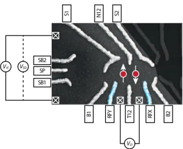
All data shown in this paper are obtained from the qubit in Refs. [32] and [1], depicted in Fig.1. This is a so-called singlet-triplet spin qubit (ST0qubit), embedded in a GaAs double quantum dot formed by electrostatic gates (the gray and blue features in Fig. 1) on top of a two-dimensional electron gas (2DEG). The ST0 qubit is encoded in the mz=0 subspace of the regime where each dot is occu- pied by a single electron, i.e., the subspace spanned by S =(|↑↓ − |↓↑) /√
2 and T0=(|↑↓ + |↓↑) /√ 2 [41], where↑or↓describes the spin state of the electron in one of the dots. This type of qubit can be fully manipulated using only electric pulses.
SB2 SP SB1
RFY T12 RFX
N12
B1 B2
S1 S2
VD
VSD Vrf
FIG. 1. False color SEM image of a device similar to the one used in this work, including the contacting scheme. Applying static voltages to the gray gates confines two electrons in a double dot potential in the 2DEG of a GaAs/Al0.31Ga0.69As heterostruc- ture. The blue gates, RFX and RFY, are used exclusively for fast manipulation. The dot on the left is used for charge sensing of the double dot and is embedded in an impedance-matching cir- cuit as the resistive element. The crossed boxes represent Ohmic contacts to the leads.
In more detail, the gates depicted in gray in Fig.1repre- sent dc static gates used to define the quantum dots and to tune them into the single-electron regime. They are heavily filtered and fed with voltages of order 1 V. The broad side gates S1 and S2 adjust the number of electrons in quan- tum dots 1 and 2. The barrier gates B1 and B2 control the tunnel coupling to the leads and the interdot coupling is controlled by the “nose” and “tail” gates, N12 and T12.
Two additional control gates (named RFX and RFY and depicted in blue in Fig.1) are used for qubit manipulation by applying millivolt-scale signals. They are dc-coupled to an arbitrary waveform generator Tektronix AWG5014C operated at 1 GS/s and attenuated by 33 dB at various cryo- genic stages to reduce thermal noise from room tempera- ture. Using dedicated static and control gates eliminates the need for bias tees and the resulting pulse imperfections [28] and ensures a nearly flat frequency response of the control gates from dc to a few hundred megahertz, at the cost of one additional gate electrode.
The double dot is capacitively coupled to a third dot (named the sensing dot), which is used as a charge detector.
Its conductance depends on the local electrostatic land- scape, which allows reading out the charge state of the double dot [42]. The spin state of the double dot can be probed through the sensing dot by spin-to-charge conver- sion based on Pauli spin blockade [43,44]. The sensing dot is embedded as a resistive component in an impedance- matching circuit, so that the conductance through the dot
can be monitored using rf reflectometry [36,37,45] at a local oscillator frequency of approximately 230 MHz and a bandwidth of 20 MHz. We employ a setup similar to that of Ref. [37], with the addition of a cryogenic circulator at base temperature. The demodulated signal Vrfis a function of the conductance of the sensing dot and is recorded using an Alazar ATS9440 digitizer board.
We typically use a hardware sample rate of 100 MS/s, which we downsample on the fly at the full data rate to 250 kHz using a multithreaded, high-throughput, C++- based driver for the Alazar card. This downsampled rate arises from a typical length of 4μs for experiments, which usually comprises a 2.5-μs-long measurement window during which we power the rf circuit. Effects of 1/f -like noise are eliminated from the data by changing the sweep- pulse parameter after each cycle and then averaging over many repetitions of the parameter sweep to elude slow drifts in the sensor or gate voltage configuration. For a typ- ical tuning data set, the sweep comprises 100 parameter values and it is repeated 1536 times for a total mea- surement time of 1536×100×4μs≈600 ms and then averaged again over 1–5 repetitions, if necessary. These acquisition parameters are not yet optimized for speed and we expect that a speed-up of at least a factor of 10 is pos- sible while still maintaining an adequate accuracy of the extracted parameters.
III. FINE TUNING OF THE QUBIT
This section describes in detail the fine-tuning of a ST0
qubit after the double dot has been tuned in the two- electron regime, either around (2,0)-(1,1) or the (0,2)-(1,1) charge transition [see Fig. 2(a)]. The procedure for the coarse-tuning to this charge regime is described in the Appendix. All measurements presented in this section are performed using rf reflectometry on the sensing dot.
-4 -2 0 2 4
RFX (mV) -4
-2 0 2 4
RFY (mV)
(a)
-4 -2 0 2 4
RFX (mV) -4
-2 0 2 4
RFY (mV)
(b)
-100 -90 -80 -70 Vrf (V)
(1, 1) (1, 0)
(2, 0)
FIG. 2. (a) Charge stability diagram of the double dot measured using rf reflectometry. Different values of Vrfcorrespond to dif- ferent charge ground states. (b) Fit of the stability diagram using the model described in Sec.III A. Circles and lines mark the auto- matically detected triple points and the positions of the charge transition. The gray arrow represents the direction of the detun- ing. In both figures, we subtracted a background value due to the direct influence of the charge sensor extracted from the fit.
A. Locating the triple points
The operation of a qubit requires the accurate character- ization of the charge stability diagram in the RFX-RFY plane (here and in the following, RFX and RFY refer to the voltage applied to the respective gate). In other words, it is necessary to know the exact position of the triple points—the points in the charge stability diagram where three charge states are energetically degenerate [e.g., (1,0); (1,1); and (2,0)]—and of the so-called lead transitions—the transitions between different charge states of the double dot that involve electron exchange with one of the reservoirs [e.g., the transition (1, 0)↔(1, 1)]. We present instead an automated routine, based on a measure- ment of the charge stability diagram near the (2,0)-(1,1) transition, followed by the fit to a simple model that allows the extraction of the relevant parameters.
The fitting model consists of two parts. The first part is a two-site Hubbard Hamiltonian without spin:
H=
⎛
⎜⎜
⎝
E1,0+v1 0 0 0
0 E1,1+v1+v2 tc 0
0 tc E2,0+2v1 0
0 0 0 E2,1+2v1+v2
⎞
⎟⎟
⎠ in the charge basis j ∈ {(1, 0),(1, 1),(2, 0),(2, 1)}. Here, Ej are the basis state energies at RFX=RFY=0, tc is the interdot tunnel coupling, and vi the on-site potential, which can be calculated knowing the voltages applied to the rf gates Vi and their respective lever arms, including cross-capacitances. The index i indicates RFX and RFY, respectively (V1=RFX and V2=RFY). The spectrum of this Hamiltonian can be calculated analytically to find the charge configuration of each eigenstate at each point in the RFX-RFY plane. Assuming that the occupation probability of each state corresponds to thermal equilibrium, we obtain a vector p, describing the occupation probabilities of the various charge basis states.
Since measurements like those presented in Fig. 2 are slow compared to the system dynamics, we can use the ground-state charge population vector p as input in a linear fitting model for the charge sensor:
S=p·s+sct,1V1+sct,2V2+S0, (1) where S is the charge sensor output, s is a vector that contains the sensor output for each charge eigenstate, sct,i
account for direct cross talk between the rf gates and the sensor, and S0 is an offset. The components of s, as well as sct,i and S0, the lever arms, the cross-capacitances, the energies Ei, and the interdot tunnel coupling tc, are treated as fitting parameters, while the input parameters for the fit are the 2D sensor output data and the voltages Viapplied to the rf gates. A typical measurement and a fit to the data are presented in Fig. 2. From the fit parameters, the position of the triple points and the location of the lead transi- tions in the RFX-RFY plane are extracted. These values
TABLE I. Typical values for the coefficients of the virtual gates. The values correspond to the ratio of change in physical gate voltages to that of the virtual gate.
Virtual gate
LeadY LeadX T N X Y
Physical gate B1 1 0 0 0 0 0
S1 −0.76 0.5 −0.52 −0.5 1.5 −2.1
T12 0 0 1 0 0 0
N12 0 0 0 1 0 0
B2 0 1 0 0 0 0
S2 0.26 −1.1 −1.25 −0.5 −3.68 1.03
are used as reference points in all of the following tuning procedures and to recalibrate the setup after a charge rear- rangement. Furthermore, the direction orthogonal to the segment where the charge states (2,0) and (1,1) are ener- getically degenerate defines the so-called detuning axis [gray arrow in Fig.2(b)]. In the following, we fix=0 to correspond to the measurement point defined in Sec.III E.
B. Setting up virtual gates
The first step of the tuning procedure is the coarse tun- ing of the double dot in the two-electron regime, i.e., the identification of the (2,0)-(1,1) [or the (0,2)-(1,1)] charge transition. This step can be based on standard quantum transport measurements (see the Appendix) or charge sens- ing, and was automated in Ref. [33]. Once the double dot has been tuned in the appropriate charge regime, the fine- tuning of the qubit can start. For doing so, it is convenient to switch to virtual gates. These virtual gates are given by a linear combination of three physical gates (see TableI) that allow tuning the parameters of the double dot while leav- ing the charge stability diagram in the RFX and RFY plane unaffected. Virtual gates are chosen such that each of them affects primarily one specific dot parameter: gates LeadY and LeadX change the tunnel coupling to the respective lead, while the tunnel coupling between the dots is manipu- lated by the virtual gates T and N . In each case, in addition to changing the physical gate that mostly influences the desired parameter, a compensating voltage is applied to the S1 and S2 gates to cancel out any cross-capacitance effect.
Virtual gates X and Y depend only on S1 and S2 and are used to readjust the position of features in the charge sta- bility diagram in the case of imperfect compensation from the virtual gates or charge rearrangements.
To obtain the virtual gate coefficients shown in TableI, we focus on the lead transitions and measure how their position in the RFX-RFY plane is shifted by the potential applied on a certain gate. To do so, we apply two different voltages (differing typically by 2–6 mV) to each of the dc gates in turn. For each set of voltages, we measure the dot’s response while sweeping RFX or RFY across both lead transitions, as shown in Fig.3(a)for the case of the Y lead.
In these curves, the two plateaus correspond to two differ- ent charge states of the double dot. The labels close to each curve indicate the gate on which the potential is changed.
To obtain the influence of that gate, the value of RFX (or RFY) at which the transition between the two plateaus occurs is extracted using a fit model corresponding to a Fermi distribution [46],
Vrf(v)=Vrf,0+δVrfv− 1 2A
1+tanh v−vlead
w
. (2) Here,vis the voltage on either the RFX or RFY sweeping gate, Vrf,0represents the background value of the charge- sensing signal Vrf, the linear termδVrfv accounts for the direct influence of the sweeping gate on the conductance through the sensor (assumed to be linear), the third term accounts for the excess charge once an electron tunnels into or out of the quantum dot and includes a finite elec- tron temperature and lever arm via w, while vlead defines the position of the lead transition, and finally A is the con- trast of the transition. We use Vrf,0,δVrf, A, w, andvlead as fit parameters. The values of vlead extracted from these fits depend on the voltage applied to all the dc gates and are used to construct a 2×6 cross-capacitance matrix.
Virtual-gate coefficients are then extracted by inverting the appropriate submatrices of the cross-capacitance matrix.
Typical values are given in TableI. The virtual-gate coef- ficients can be further fine-tuned by applying the same principle to study the influence of the dc gates on the loca- tion of the triple points of the (2,0)-(1,1) charge transition or on the position of the ST+anticrossing.
A similar concept is used in Ref. [2] to perform orthog- onal charge stability diagrams in a three-electron quantum dot, and in Refs. [29] and [47].
C. Tunnel coupling to the leads
The next step is the tuning of the tunnel coupling to leads X and Y (Ohmic contacts next to the rf gates; see Fig.1), which act as electron reservoirs. The coupling to these
-3 -2 -1 0 1 -6
-4
Tunnel coupling width: 210 µV
0 2 4
-2 0 2
4tl1/tl2 for X Lead: 33/28 ns
0 2 4
-6 0 4
tl1/tl2 for Y Lead: 210/490 ns
(mV)
(a) (b)
(d) (c)
Vrf (V)Vrf (V)
t ( μs)
t ( μs)
ε
-1 0 1
RFX (mV) Virtual gates
S1 T12 S2 B2
FIG. 3. (a) To determine the influence of the various dc gates on the position of a lead transition, we apply two different voltages to each one of the dc gates in turn. For each set of voltages, we measure the occupation of the double dot as we sweep across two regions in the charge stability diagram.
(b),(c) To measure the tunneling times to the leads, we apply megahertz-frequency square voltage pulses across the respec- tive lead transition, forcing an electron to be exchanged with the respective reservoir. The tunneling time can be extracted from the rise time of the response signal. (d) The interdot tunnel cou- pling is extracted by sweeping along the detuning, recording the average charge occupancy, and measuring the broadening of the transition.
leads is controlled by the virtual gates LeadY and LeadX , and it must be weak enough to prevent excess T1relaxation due to cotunneling or thermal activation and, at the same time, be strong enough to allow fast qubit initialization within tens of nanoseconds.
To extract the tunneling time to the X lead, we apply 25- MHz square-wave pulses that force the system to switch between the charge states(1, 0)↔(1, 1)[or, equivalently, between(2, 0)↔(2, 1)] and use the sensing dot to mea- sure the time-dependent occupation of the double dot. For this purpose, we average the signal over approximately 1500 periods, recorded at a hardware sampling rate of 100 MS/s. A typical time trace is shown in Fig.3(b). Apply- ing the square-wave pulses to regions of charge stability (i.e., where no charge transition is possible) allows us to subtract the background due to direct sensor coupling. The tunneling time to the lead can be extracted from the rise times of the response to the square pulses [Fig.3(b)], with a lower sensitivity bound of about 25 ns determined by the bandwidth of the tank circuit attached to the sensing dot (faster tunneling times can be resolved with the reload sweep discussed in Sec.III E). To fit these data, we use the
model Vrf(t, t0)
=
⎧⎪
⎪⎪
⎨
⎪⎪
⎪⎩ Vrf,0+1
2Acosh t0/2tl,1
−exp
(t0−2t)/2tl,1 sinh
t0/2tl,1
for t<t0, Vrf,0−1
2Acosh t0/2tl,2
−exp
(t0−2t)/2tl,2
sinh
t0/2tl,2 for t≥t0, (3) where t0=2 μs is the half-period of the square pulse. It produces an exponential rise and decay of the average sen- sor signal with time constants tl,1 and tl,2 whenever the gate voltage is changed. The prefactors and offsets of the exponential rise and decay are derived from the require- ment that the curve be continuous. The same procedure is used to extract the tunneling times to lead Y, with the only difference that now the square pulse has to force transi- tions between the charge configurations(1, 0)↔(2, 0)[or (1, 1)↔(2, 1)].
Typical target values for tl,1(2) range from 25 to 50 ns.
Importantly, since all initialization methods addressed here require only tunneling to one lead (see Secs. III E–III F), the barrier to the other lead can be made less transparent to reduce relaxation [Fig.3(c)].
D. Interdot tunnel coupling
The tunnel coupling tc between the two dots is mostly controlled by the N and T virtual gates. It determines the strength of the exchange interaction between the two electrons and, therefore, the energy splitting J()between the singlet S and the triplet T0 in the (1,1) configuration.
In order to characterize the tunnel coupling, we mea- sure the broadening of the interdot transition between the (2,0)-(1,1) charge configuration by sweeping the detun- ing orthogonally across the (2,0)-(1,1)-transition [see Fig.2(a)] and recording the average charge state [46], as shown in Fig. 3(d). We typically measure each detuning step for 1 μs and average over 4000 scans for a total measurement time of 0.4 s. For simplicity, we extract the broadening of the transition by fitting Eq. (2) to the data, rather than using the physically correct model of an avoided crossing, as we find the difference between the two approaches to be marginal. The value extracted for the effective temperature w now represents the interdot tunnel coupling tc. Good values for tcfor the operation of the qubit range from 18 to 24μeV, using an estimated lever arm of 9.8 V/eV. Smaller values of the tunnel coupling would lead to Zener tunneling when sweeping through the (2,0)-(1,1) transition and, therefore, should be avoided.
This characterization method is limited by temperature broadening, which, in our setup, prevents tunnel couplings below 9 μeV from being resolved. A similar approach to ours is used in Refs. [34] and [35] for an automated
tuning of the interdot tunnel coupling, whereas an alterna- tive approach for determining the interdot tunnel coupling based on time-resolved charge sensing is described in Ref. [48]. Furthermore, the tunnel coupling can also by extracted by photon-assisted tunneling spectroscopy [49].
Compared to the presented method, both alternatives are time consuming and, thus, less attractive for our purposes.
E. Locating the measurement point
The operation of a qubit relies on the ability to reliably initialize the qubit in a well-known state and to accurately measure the qubit’s final state [50]. Historically, the stan- dard approach for initializing a spin qubit in a singlet state is based on the transition cycle T(1, 1)→(1, 0)→ S(2, 0), which requires electron exchange with both reser- voirs [44] [here and in the following, the notation S(n, m) and T(n, m)indicates the singlet and the triplet state in the (n, m) charge configuration, respectively]. Here, we present a modified version that only relies on tunnel coupling to one lead. Compared to the old approach, this proce- dure requires less tuning and enables simpler future device layouts. It also allows for an enhanced charge-detection readout scheme [51] to counteract the visibility loss at high-magnetic-field gradients [52].
We first need to locate the region of metastable (1,1) triplets within the (2,0) ground-state charge configuration, i.e., the area around point M in Fig.4(a). The latter repre- sents a high-resolution charge-stability diagram, indicating the thresholds of the relevant transitions. To identify the region of metastable (1,1) triplets, we repeatedly apply the pulse scheme M -R1-R2-M , while sweeping through the RFX-RFY plane by adding a dc offset to the rf gates, and waiting for 200 ns at points R1 and R2[44,53]. Data acquired during the pulse sequence are discarded and we read out the state of the system only at the final point M . If, during a scan, point M falls deep into one of the charge-stability regions, we then simply observe the same response as in a charge scan without pulses applied (see Fig.2). However, if the pulse sequence M -R1-R2-M drives the system through three stability regions as indicated in Fig. 4(a), the measured signal will then have a value between the one corresponding to the (2,0) charge state and that of the (1,1) state. The reason is that when we step from R1to R2, we initialize at random either a singlet S(2, 0)or a triplet T(2, 0)state. If the system is in the T(2, 0)state, then it tunnels into the (1,1) configuration when we step back to point M . Vice versa, if the system in R2is in the S(2, 0)state, it remains in this state. In this way, we map out the so-called measurement triangle (or trapezoid, if the singlet-triplet splitting is smaller than the interdot charge coupling, as in Fig. 4), i.e., the region of the RFX-RFY plane where Pauli spin blockade allows for spin-to-charge conversion.
RFX (mV)
RFY (mV)
-4 -2 0 2 4
4
2
0
-2
-4 -40
-35 -30 -25 -20 -15
S(2,0) (1,0)
(1, 1) (1, 0)
(2, 1)
M T+
ST+ S
R1
R2
T(2,0) (1,0)
(1, 1) (2, 1)
SL
SL
T0
T0 S SL S SL
SL
(a) (b)
(1,1) T(2,0)
(1,1) S(2,0)
Energy
componentVia
J (2, 0)
S
T
Vrf(V)
RFX (mV)
RFY (mV)
-4 -2 0 2 4
-4 -3 -2 -1 0 1 2 3 4
RFX (mV)
RFY (mV)
6 5 4
-4 -2 0 2 4
-4 -3 -2 -1 0 1 2 3 4
M S
R1
R2
M
R1 R2
S
(c) (d) Vrf (V)
FIG. 4. (a) High-resolution charge-stability diagram around the (2,0)-(1,1) transition used to define the two-electron spin qubit.
Important points used to initialize the qubit in different states and for measurement are marked by dots and further explained in the main text. Transitions are labeled in white. (b) Diagram showing the energy relaxation cascade used to initialize the (1,1) ground state|↑↑at point T+(see Secs.III F). SL⊗ ↓(↑)denotes the state of a singlet state in the left quantum dot and a down (up) state in the right dot. Arrows indicate relaxation via electron exchange with the (2,1) charge configuration. (c) Charge stabil- ity diagram measured using the pulse sequence M -R1-R2-M (see Secs.III E). The measurement trapezoid appears as an area where the readout signal Vrfis between the values corresponding to the S(2,0) and to the (1,1) configurations (yellowish turquoise area).
The blurred boundaries of the readout trapezoid reflect a fail- ure of the random load pulse sequence rather than instabilities.
(d) Adding a waiting time at point S after the pulse sequence from (c) maps out the “mouse bite” (yellow area within the mea- surement trapezoid), i.e., the region of singlet reload within the measurement triangle (see Sec.III E).
To determine the position of the singlet reload point, we extend the pulse scheme to M -R1-R2-M -S-M [see Fig. 4(c)], by including an additional 100-ns pause at point S. When point S stays energetically between the (1,1)-T(2,0) and (1,1)-S(2,0) transitions (see Fig.2), then electron exchange with the Y reservoir will lead to the initialization of a (2,0) singlet state. If this is the case, mea- suring the state of the system back at point M will give a value of Vrfcorresponding to the (2,0) charge state, instead of the intermediate value observed with the M -R1-R2-M pulse scheme. Scanning the position of the pulse cycle over
0 200 400 2
6
-2 0 2
0 5
T+ position: -1270 μV
0.2 0.6 1
1 4
ST+ position: 540 μV
ε (mV) δT(mV)
t (ns)
(a)
(d) (c)
δS(mV) Vrf (V)Vrf (V)
-1 0 1
2 6
Load position (b) Load time: 22 ns
FIG. 5. (a) To determine the optimal position of the singlet reload point, we shift the position of point S in the pulse sequence M -R1-R2-M -S-M along the directionδS[see text and Fig.4(a)].
The optimal position for S is in the middle of the plateau of low Vrf values. (b) The singlet reload time is extracted by applying the pulse sequence M -R1-R2-M -S-M and measuring the triplet return probability as a function of the waiting time t at point S.
(c),(d) The positions of the T+reload point and of the ST+tran- sition can be determined using the pulse sequences described in Secs.III FandIII G, respectively, and result in peaks in the mea- sured Vrfsignals as a function of the displacementδTand of the detuning.
the RFX-RXY plane (the relative position of the points M , R1,2and S is kept fixed) maps out the area known as
“mouse bite,” visible in see Fig.4(d).
Once the mouse bite has been identified, we also know a suitable position of point S for fast initialization of the qubit in the S(2,0) state. To further optimize the position of S, we repeat the pulse sequence M -R1-R2-M -S-M , but now sweeping the position of point S perpendicularly to the (2,0)-(1,0) transition line, while keeping all other points of the sequence fixed. In particular, point M has to lay within the mouse bite. As before, we measure the state of the system only in the final point M . The response sig- nal Vrf shows a plateau as a function of the position of point S, at the signal level of the (2,0) charge ground state;
see Fig. 5(a). The two ridges where the signal increases represent the onset of the transitions (1,0)→ S(2,0) and (1,0)→ T(2,0), respectively. The optimal position of point S for the operation of the qubit lays symmetrically between these two points.
In a last characterization scan, we fix point S at the optimal position and repeat the pulse sequence M -R1-R2-M -S-M , now varying the waiting time t at point S. Again, we measure the state of the system only in the
final point M . The longer we wait at point S, the higher the probability to initialize a singlet S(2, 0)and, therefore, the lower the value of Vrf measured at point M , see Fig.5(b).
We fit these data with a simple exponential decay:
Vrf(t)=Vrf,0+Ae−tloadt , (4)
where Vrf,0, A, and tloadare fit parameters. For a well-tuned dot, the singlet reload time tloadtypically lies in the range of 10 to 50 ns. This characterization scan is complementary to the one presented in Sec.III C. It exploits the full time resolution of 1 ns of the AWG, as it is not limited by the bandwidth of the readout tank circuit.
Having identified an optimal singlet reload point and characterized the singlet reload time tload, in the rest of this paper, whenever we write “initializing the qubit in the sin- glet S(2,0) state,” we mean the following procedure: (i) go to the optimal point S, (ii) wait in this position for approx- imately 5 tload, and (iii) move to measurement point M . Note that this initialization procedure requires only elec- tron exchange with one lead, which means that only one tunnel barrier has to be tuned to find an optimal operation regime. Moreover, the initialization time is simply given by the tunnel coupling to this lead and can be as fast as a few tens of nanoseconds.
F. Locating the triplet T+reload point
A fundamental technique for the operation of qubits based on GaAs is dynamical nuclear polarization (DNP).
This technique is used for stabilizing the surrounding bath of nuclear spin and relies on the ability to initialize the (1,1) ground state T+[28]. Originally, the T+initialization was done by exploiting both the (2,1)-(1,1) and the (1,0)-(1,1) transitions, i.e., allowing electron exchange with both leads [38]. Here, we report a different approach, again based on tunneling only to one lead. The trick is to exploit the relax- ation cascade shown in Fig.4(b), which characterizes the region of the stability diagram close to the (1,1)-(2,1) tran- sition. In the presence of an external magnetic field Bext, the triplet T+represents the ground state of the (1,1) charge configuration and transitions from the (2,1) ground state to the excited states of the (1,1) configuration are not ener- getically allowed close to the (1,1)-(2,1) boundary. Hence, if we initialize the qubit in the S(2,0) state, and then pulse to a point T+ close to the (1,1)-(2,1) transition [see Fig.
2(a)], the qubit will either go directly into the T+state or it will eventually reach this state at the end of the relax- ation cascade sketched in Fig. 2(b). Importantly, for this to happen, we need to ensure that the exchange interaction satisfies the requirement Bext >J() > Bz, which is nec- essary for having sufficient mixing between the|↑↓,|↓↑
states and the full relaxation to the T+ground state. Here, Bz is the difference of the magnetic field in the two dots.
To find the optimal T+reload point in the charge stabil- ity diagram, we perform the following sweep. We initialize
the qubit in the S(2,0) state and then pulse to point T+ without crossing the upper triple point to avoid measure- ment artifacts. The distance between T+ and the upper triple point has to be chosen so as to fulfill the energy requirement Bext >J() > Bz. After a waiting time of 100 ns to allow energy relaxation, we switch back to the measurement point M and measure the state of the sys- tem. We repeat this procedure while sweeping the position of point T+byδT, perpendicularly to the direction of the (1,1)→(2,1) transition [Fig.4(a)]. The optimal position of point T+appears as a maximum of Vrf as a function ofδT
[see Fig.5(c)], indicating that a triplet is initialized while waiting at point T+. To extract the exact position of the reload point, we use a phenomenological model motivated by Eq.(2)and given by
Vrf(δT)=Vrf,0+ 1 2A1
1+tanh δT−δtl,1
w
−1 2A2
1+tanh δT−δtl,2
w
(5) to fit the data. The position of the T+point is then given by (δtl,1+δtl,2)/2.
G. Locating the ST+transition
In addition to the location of the T+-reload point, it is also necessary to know the location of the S-T+anticross- ing to perform DNP. To find the latter, we follow Ref.
[43] and initialize the qubit in the singlet state, change the detuning, wait 100 ns at a given detuning, and then return to the measurement point and read out the final qubit state.
When the detuning is at the S-T+anticrossing, the hyper- fine and the spin-orbit interaction can turn the initialized S state into a T+ state, giving rise to a maximum in the measured Vrf as a function of. Because the location of the ST+transition strongly depends on the local magnetic field, any unintentional polarization, for example, due to hyperfine mediated spin flips at the ST+ transition, shifts the precise position of the anticrossing. To avoid this prob- lem, we include pauses of a few milliseconds at the end of eachsweep, to allow any unintentional polarization to relax. If needed, we average over a few different sweeps and fit our data with a Gaussian model
Vrf()=Vrf,0+δVrf+Ae−(−stp)2/2w2 (6) to extract the positionstpof the ST+transition (Vrf,0,δVrf, A,stp, and w are fit parameters).
Not only is this position crucial for the pulsed DNP scheme but, in combination with the T+ reload point, it is also used as an anchor point in the charge stability dia- gram. Adjusting the dot using the X and Y virtual gates to obtain the same values for the ST+ and T+ scan after a small charge–switching event usually restores all quan- tum dot parameters and results in the same J() relation.
Furthermore, the position of the ST+ crossing is used to automatically determine switching events [20,54,55] that shift the whole transition by several mV.
H. Tuning workflow
To summarize, once the (2,0)-(1,1) charge transition has been identified, the typical fine-tuning workflow of a ST0
qubit starts by defining the virtual gates. The next step is to bring the tunnel couplings to the leads in the right regime.
Then, the singlet reload point S and the measurement trian- gle are determined. The energy splitting J()of the qubit is subsequently tuned by adjusting the inter-dot tunnel cou- pling. A working scan of the S-T+transition as described in Secs.III Gis a good indicator of a suitable interdot tun- nel coupling for the operation of the qubit. Usually, tuning the tunnel couplings is an iterative procedure, as adjusting the T and N virtual gates used to tune the interdot coupling also affects the coupling to the leads a little. Finally, the position of the T+reload point is determined. During the whole tuning procedure, we periodically check the exact position of the (2,0)-(1,1) transition by recording a charge stability diagram. The triple points, which act as anchor points, are extracted automatically by a fit that includes a model of the charge transition, as described in Sec.III A.
The lower triple point is used as a reference for the mea- surement point and either an offset on the rf gates or on
SB2 (V)
SB1&SP (V)
-0.32 -0.3 -0.28 -0.26 -0.24 -0.22 -0.49
-0.48 -0.47 -0.46 -0.45 -0.44 -0.43 -0.42 -0.41 -0.4 -0.39
-0.2 -0.15 -0.1 -0.05 0 0.05 0.1 0.15 0.2 0.25 Vrf (V)
FIG. 6. Characteristic charge-stability diagram of the sensing dot, measured with rf reflectometry. Depending monotonically on the conductance through the dot, Vrfshows Coulomb oscilla- tions once the source and drain barriers are sufficiently opaque.
Tuning the sensor to a sensitive position (see circle) allows for charge sensing of the nearby double quantum dot.