Tailoring neuroelectronic interfaces via combinations of oxides and molecular layers
Inaugural-Dissertation zur
Erlangung des Doktorgrades
der Mathematisch-Naturwissenschaftlichen Fakultät der Universität zu Köln
vorgelegt von
Xiaobo Yuan aus Shandong, China
Gutachter: Prof. Dr. Roger Wördenweber Prof. Dr. Berenike Maier
Tag der mündlichen Prüfung: 06.01.2021
Abstract
In this work we introduce a novel method to tailor the interface of neuroelectronic devices in a way that (i) it becomes biocompatible and (ii) at the same time allows a guided growth of neurons on the substrate. By using different oxides which are functionalized with the organic molecules 3-aminopropyltriethoxysilane (APTES), we can generate areas onto which neurons either adhere, grow and mature, or preferably don’t adhere. Furthermore, the resulting cell-chip interface is extremely thin (molecular monolayer) and robust, and therefore promises an optimal electronic signal transfer in neuroelectronic devices.
In a first step, surface potential analyses are used to record and optimize the gas-phase deposition of self-assembled monolayers (SAMs) of APTES on SiO2 and to determine the resulting change of the electrokinetic potential and charge at the solid-liquid interface. We found that (i) an adequate post-deposition treatment is crucial to the formation of perfect molecular APTES SAMs. (ii) The activation state of the SiO2 surface which determines the amount of binding docking sites for the molecules, and the stability of the APTES coating is characterized by electrokinetic potential measurement.
In a second step, we demonstrate that cell adhesion and neuron maturation can be guided by patterned oxide surfaces using different oxides functionalized with an organic molecular layers of APTES. It seems that only physisorbed layers (no chemical binding) can be achieved for some oxides (Ta2O5 and TiO2), whereas self-assembled monolayers (SAM) form on other oxides (SiO2 and Al2O3). As a result of the different types of APTES binding and the difference in the electrokinetic potential,a large cell density contrast is obtained for SiO2 and Ta2O5. The cell density and coverage with dendrites and growth cones are ~ 8 respectively ~ 3.2 times larger on SiO2 compared to Ta2O5 both coated with APTES.
Finally, we test the different oxides in multi electrode array (MEA) devices using the different oxides (Al2O3, TiO2, Ta2O5) as passivation and at the same time for the guidance of cell growth. Impedance measurements indicate, that, due to the thinness of the passivation, the feedlines strongly couple into the electrolyte. Nevertheless these novel MEAs work perfectly in HL-1 cell culture experiments showing smaller action potential signals but at the same time a signal-to-noise ratio (SNR≈3) which is comparable to conventional polyimide passivated MEAs. Finally, tests with neuronal cell cultures show guided cell adhesion, however the patterns chosen for the cell guidance in these experiments turn out to be too small to allow the development of neuronal networks.
In conclusion, the combination of organic SAMs and patterns of different oxides (especially SiO2 and Ta2O5) allows guided neuron cell growth. Simultaneously the oxide
can be used as passivation in neuroelectronic devices. This complete package could represent a promising option for the development of robust neuroelectronic devices that might enable guided neuron growth as well as a good cell-chip communication.
Zusammenfassung
In dieser Arbeit stellen wir eine neue Methode vor, um die Schnittstelle von neuroelektronischen Bauelementen derart anzupassen, dass sie (i) biokompatibel wird und (ii) gleichzeitig ein geführtes Wachstum von Neuronen auf dem Substrat ermöglicht. Durch die Verwendung unterschiedlicher Oxide, die mit dem organischen Moleküle 3- Aminopropyltriethoxysilan (APTES) funktionalisiert werden, können wir sowohl Oberflächen erzeugen, auf denen Neuronen anhaften, wachsen und reifen als auch solche, an denen sie vorzugsweise nicht anhaften. Darüber hinaus ist die resultierende Zell-Chip- Schnittstelle extrem dünn (molekulare Monolayer) und robust und verspricht daher eine optimale elektronische Signalübertragung in neuroelektronischen Geräten.
In einem ersten Schritt werden Oberflächenpotenzialanalysen zur Erfassung und Optimierung der Gasphasenabscheidung von Self-Assembled Monolayers (SAMs) von APTES auf SiO2 und zur Bestimmung der resultierenden Änderung des elektrokinetischen Potenzials und der Ladung an der Fest-Flüssig-Grenzfläche eingesetzt. Wir fanden heraus, dass (i) eine adäquate Nachbehandlung nach der Abscheidung der Moleküle entscheidend für die Bildung perfekter molekularer APTES-SAMs ist. (ii) Der Aktivierungszustand der SiO2-Oberfläche, der die Anzahl der Andockstellen für die Bindung der Moleküle und die Stabilität der APTES-Beschichtung wiedergibt, wird durch die Messung des elektrokinetischen Potentials charakterisiert.
In einem zweiten Schritt zeigen wir, dass Zelladhäsion und Neuronenreifung durch strukturierte Oxidoberflächen unter Verwendung verschiedener Oxide, die mit einer organischen Molekularschicht aus APTES funktionalisiert sind, gesteuert werden können.
Es scheint, dass für einige Oxide (Ta2O5 und TiO2) nur physisorbierte Schichten (keine chemische Bindung) erzielt werden können, während sich auf anderen Oxiden (SiO2 und Al2O3) selbstorganisierte Monoschichten (SAM) bilden. Infolge der verschiedenen Arten der APTES-Bindung und des Unterschieds im elektrokinetischen Potential ergibt sich für SiO2 und Ta2O5 ein großer Zelldichtekontrast. Die Zelldichte und die Bedeckung mit Dendriten und Wachstumskegeln ist auf SiO2 ~ 8 bzw. ~ 3,2 mal größer als auf Ta2O5, beide wurden mit APTES beschichtet.
Schließlich testen wir die verschiedenen Oxide in Multi-Elektroden-Arrays (MEA) mit den unterschiedlichen Oxiden (Al2O3, TiO2, Ta2O5) als Passivierung und gleichzeitigen Steuerung des Zellwachstums. Impedanzmessungen zeigen, dass aufgrund der Dünnheit der Passivierung die Zuleitungen stark in den Elektrolyten einkoppeln. Dennoch funktionieren diese neuartigen MEAs in HL-1-Zellkulturexperimenten einwandfrei. Sie zeigen zwar kleinere Aktionspotentialsignale, aber besitzen gleichzeitig ein Signal-
Rausch-Verhältnis (SNR≈3), das mit herkömmlichen polyimid-passivierten MEAs vergleichbar ist. Abschließend zeigen Versuche mit neuronalen Zellkulturen eine geführte Zelladhäsion, jedoch erweisen sich die für die Zellführung in diesen Experimenten gewählten Strukturen als zu klein, um die Entwicklung neuronaler Netzwerke zu ermöglichen.
Zusammenfassend lässt sich sagen, dass die Kombination von organischen SAMs und Strukturen aus unterschiedlichen Oxiden (insb. SiO2 und Ta2O5) ein geführtes Neuronenzellwachstum ermöglicht. Gleichzeitig kann das Oxid als Passivierung in neuroelektronischen Bauelementen verwendet werden. Dies Gesamtpaket könnte ein vielversprechender Weg für die Entwicklung robuster neuroelektronische Bauelemente sein, die ein geführtes Neuronenwachstum sowie eine gute Zell-Chip-Kommunikation ermöglichen könnten.
CONTENTS
1. Introduction... 1
2. Theoretical background and state of the art ... 5
2 .1 Cell-substrate interface ... 5
2.1.1 Cell-substrate adhesion ... 6
2.2 Engineering the cell-substrate interface ... 7
2.2.1 Engineering the cell-substrate interface towards biocompatibility ... 7
2.2.2 Engineering the cell-substrate interface towards guided growth ... 8
2.3 Surface functionalization with organic SAMs ... 13
2.3.1 Silane SAM on oxides ... 14
2.3.2 The role of the functional group ... 17
2.4 Electronic cell-chip coupling ... 19
2.4.1 Action potential and cell-electrolyte interface ... 20
2.4.2 Electrode-electrolyte interface ... 22
3. Sample preparation, characterization and experimental techniques ... 26
3.1 Deposition techniques ... 26
3.1.1 Molecule layer deposition ... 26
3.1.2 Atomic layer deposition ... 29
3.1.3 Electron beam evaporation ... 31
3.2 Lithography and lift-off technique ... 32
3.2.1 Design ... 32
3.2.2 Lithography and lift-off ... 33
3.2.3 Etching ... 35
3.3 Characterization methods ... 38
3.3.1 Ellipsometry ... 38
3.3.2 Contact angle measurements... 39
3.3.3 Surface potential measurement ... 41
3.3.4 X-ray photoelectron spectroscopy ... 43
3.3.5 X-ray diffraction ... 44
3.3.6 Scanning electron microscope ... 45
3.3.7 Fluorescence microscopy ... 46
3.4 Cell culture ... 48
3.4.1 Cortical neuron culture ... 48
3.4.2 HL-1 cell culture ... 49
3.4.3 Live-dead staining ... 49
3.4.5 Critical point drying ... 50
3.5 Electrical characterization ... 51
3.5.1 Multi electronic arrays ... 51
3.5.2 MEA Encapsulation ... 52
3.5.3 BioMAS ... 52
4. Results and discussion ... 54
4.1 Vapor-phase deposition and electronic properties of APTES SAMs on SiO2 ... 55
4.1.1 Deposition of self-assembled APTES monolayers ... 56
4.1.2 Titration analysis ... 62
4.1.3 Evaluation of the electrokinetic charge ... 63
4.1.4 Conclusion ... 67
4.2 Guided neurons growth on patterned functionalized oxides ... 68
4.2.1 Functionalization of different oxides with APTES ... 69
4.2.2 Neuronal cell growth on SiO2 and Ta2O5 ... 72
4.2.3 Guided cell growth on patterned oxides ... 76
4.2.4 Conclusion ... 80
4.3 Cell-chip coupling on ALD passivated MEAs ... 82
4.3.1 Development and characterization of MEAs ... 82
4.3.2 Cell chip coupling for the different MEAs ... 90
4.3.3 Neuron cultures on ALD MEAs ... 98
4.3.4 Conclusion ... 100
5. Conclusion and outlook ... 102
References ... 105
Erklärung ... 115
Acknowledgements ... 116
Lebenslauf ... 118
1. Introduction
1
1. Introduction
Already in the ancient times, human beings have tried to replace nonfunctional or damaged parts of their bodies. Even though less knowledge on medical sterilization, or foreign body reaction was present, people used different materials like wood or metals as substitute of arms or legs. For instance, Marcus Sergius, a Roman general, was the first recorded person in the history using a prosthesis. His right hand was cut in the Second Punic War (218 to 201 BC) and replaced by an iron hand as a substitution to hold his shield. In fact, many East Asia people, with their different culture background compared with Europe, are deeply impressed by the famous pirates’ character captain Hook (originate from the famous pirate Edward Thatch) with his wooden prosthetic leg and metal hook. For sure, by that time, the refunction of the human bodies via this simple prosthesis was strongly limited.
However, even with the development of modern technology the functionality of modern prostheses are still very limited. This could change, if prostheses could be directly addressed by the nervous system of the body. The signal transfer from sensors in the prosthesis to the nervous system would be the ultimate step for a perfect substituting prosthesis. This innovation would require a perfect and stable neuroelectronic interface between prosthesis and neurons of the human body.
Figure 1.1 Schematic of the different fields of neuroelectronic applications, ranging from brain function investigation, bionic prosthesis, artificial skin, in vivo invasive shank and biosensor, all the listed neuroelectronics request or pose a strong demanding of the interface. Individual images are taken from [1-6].
1. Introduction
Neuroelectronic devices, for example neurocognitive prostheses, which can sense or modulate neuron function in order to reconstitute or improve moving functions or cognitive processes, have been largely investigated. Implantable neurocognitive brain-computer interfaces have been proposed to help treatments of strokes, brain injuries and Alzheimer’s diseases. These devices have to be able to transfer signal information between neuron cells and the electronic implants. Also, artificial skin in combined with implanted sensors can help a person to get back the sense of feeling and touching by picking up the signal via sensors and feed it into the nervous system. In fact, the application of neuroelectronic devices is quite broad, ranging from the investigation of human brain function, controlling of prosthetic limbs, wearable artificial skin, deep brain stimulation probes and various lab- on-chip biosensors for monitoring the health condition (Figure 1.1).
However, in despite of the fruitful prospect of the neuroelectronic devices, the most serious obstacle for most applications is given by the interface between the electronic and the cell.
This interface has to fulfil a number of important requirements:
It should enable a good cell-electrode coupling, which allows a suitable transfers of the signal information between the cells system and the external device.
It should be biocompatible (non-toxic) and not lead to foreign body response (FBR).
It should be robust and withstand a long-term use.
With the purpose to achieve this aim, quite a lot of approaches have been tested. The most representative techniques are based on:
Modification of the surface of the electronics with extracellular matrix (ECM) proteins for instance, laminin, collagen or fibronectin or
Tailoring the surface of the electronic contact with polypeptides like ploy-L-lysine (PLL) and ploy-D-lysine (PDL).
Although ECM proteins and polypeptides are probably the most natural way to functionalize the surface, they still have drawbacks, for instance:
ECM proteins are macromolecules which will lead to a few hundred nanometer [7]
distance between sensing electrodes and cells. Moreover, ECM proteins can easily change their conformation and become denatured in a harsh environment at the electrode.
Polypeptides (Ploy-L-lysine (PLL) and Ploy-D-lysine (PDL)) also lead to a considerable distance between cells and electronics [8] and since it is only physically adsorbed, it easily peels off with the cells and, thus, strongly reduces the contact.
1. Introduction
3
An Alternative is given by a coating of the electronic contact with a self-assembled monolayer (SAM). This layer can form a thin, stable, robust, reusable and biocompatible surface for neuronal devices, as shown in this work. SAMs of organic molecules are monolayers of a typical thickness of nanometer or below. They can be used to mimic the ECM proteins for neuron adhesion.
Figure 1.2 Scope of this work, aiming a guided neuronal networks and starting with the analyses of the SAM formation, guided neuronal growth on different APTES coated oxides, finally, the test of neuroelectronic patterns. Neuronal networks’ image taken from [9].
In this work, we demonstrate that neuroelectronic interface can be tailored via combinations of oxides and SAMs of a short and simple organic molecule (3- aminopropyltriethoxysilane (APTES)) to obtain areas of different oxides onto which neurons either adhere or preferentially not adhere. This way we obtain a robust, reusable interface for guided cell growth, which provides a good and stable cell adhesion at predefined areas, for example, the electronic contacts. The precondition including the growth of the SAMs, comparison of different oxides and their cell compatibility are pioneered and discussed in this work.
This work is structured in the following parts:
Chapter 2 provides fundamentals of the theoretical background relevant to this field, starting with the cell-substrate adhesion process, techniques to improve the cell adhesion
1. Introduction
ability of surfaces, patterning technologies for guided cell growth, basic information on the formation of SAMs, and the properties of cell-substrate interface.
Chapter 3 describes the fabrication and patterning techniques, characterization methods and cell culture recipes used in this work.
Chapter 4 represents the discussion of the results separated in three sections (Figure 1.2):
Chapter 4.1 discusses the formation and electronic characterization of monolayers of APTES on SiO2.
Chapter 4.2 shows a guide neurons growth on test structures fabricated by patterned and oxides functionalized with APTES.
Chapter 4.3 investigates the cell-chip coupling for HL-1 cells and guided cell growth for rat cortical neurons on a new concept of neuroelectronic devices - ALD oxide passivated MEAs.
Chapter 5 provides the results and an outlook for future improvements.
2. Theoretical background and state of the art
5
2. Theoretical background and state of the art
In general, interfaces play a very important role in bioelectronics. Especially in neuroelectronics, the interface between cells and the inorganic electronics has to be robust, biocompatible, and should also allow a large electronic signal transfer, which requires adequate mechanical, chemical as well as electronic properties of the interface. This leads to a strong requirement in engineering suitable neuroelectronics interfaces for the guided cell growth on substrates and electronic devices.
In this chapter, we will highlight the theoretical background and state-of-art of engineering the cell-substrate interface. Starting with the fundamental information concerning cell- substrate interface in chapter 2.1, the state-of-art of engineering the interface is shown in chapter 2.2. In chapter 2.3 we offered a detailed introduction to self-assembled molecules that can be used to fabricate thin films and coatings with on-demand tailored compositions and architectures in a highly controlled way. Finally in chapter 2.4, the basic information of electronic cell-chip coupling is shown.
2 .1 Cell-substrate interface
Cell-substrate interfaces are essential in cell communication and stimulation, and are of fundamental importance in the development and maintenance of tissues. A huge amount of investigation has been developed on the factors that could have an impact on the cell- substrate interface, including the surface chemistry, topography, mechanical property and stiffness. These physical and chemical factors affect the adhesion, spreading and shape of the cell [10].
Since the micro-fabrication techniques which was initially developed in semiconductor and electronics industry, came into use for the study of the cells’ behavior on micro- and nano- structured surfaces a few decades ago [11]. Many studies are performed to investigate the interaction between cell and surfaces [12-19]. It turned out that cellular functions can be affected and sometimes even improved by mimicking the extracellular matrix (ECM) molecules. Thus the substrate can not only be used as a support but also guides cell adhesion, proliferation, and spreading due to physical or chemical stimulations [15].
Depending on the cell type, pattern size and geometry, stiffness and chemical properties of the substrate, substrate topography can affect the cellular functions [20]. Furthermore, nanoscale topographies affect the cell growth directly since they possess a similar size compared to ECM proteins like fibronectin, collagen and laminin [20].
2. Theoretical background and state of the art
2.1.1 Cell-substrate adhesion
Cell adhesion represents the cell’s ability to stick to another cell, an extracellular matrix (ECM) or a bare substrate. The affinity of cells to a substrate represents an important issue for the design and development of biomaterial. In a static medium culture, the process of cell adhesion can be subdivided into three stages (Figure 2.1):
(i) Initial attachment of the cell to the substrate, (ii) Flattening and spreading of the cell,
(iii) Formation of a focal adhesion of the cell on the substrate.
Figure 2.1: Schematic of the different phases of cell-substrate adhesion, adapted from [21].
Phase I: The adhesion property of cells in stage I is dominated by electrostatic interaction that is mainly due to the fact that the glycoproteins on the cell membrane are negatively charged compared to the substrate, therefore a positive charged surface is more attractive to the cells. Studies show that moderately hydrophilic surfaces lead to a better adhesion, spreading, proliferation, and differentiation of cells on a surface [22, 23]. For example, the attachment and spreading of osteoblast and fibroblast can be enhanced when the substrate’s surface is positively charged compared to negative and neutral [24].
Phase II: Following the initial attachment, cells continue to flatten and spread on the substrate, resulting in a decrease of cell height and an increase of contact area. For example, the contact area of rabbit articular chondrocyte with the substrate increases by a factor 3 within 6 h [25].
Phase III: Finally in this process of adhesion, the cell spreads beyond the area of the spherical cell. This spreading process requires a continuous adhesion process with reorganization and distribution of the skeleton around the cell’s body edge. The cells will finally reach their maximum spread area via expansion and reaching a strong adhesion [21, 26].
2. Theoretical background and state of the art
7
2.2 Engineering the cell-substrate interface
As indicated before, there are many factors that affect the cell adhesion, such as surface chemistry, topography, stiffness and so on. By changing one or more of these factors, the cell-substrate affinity properties can be modified. In fact, for neuroelectronic applications, the engineering of the cell-substrate interface has been widely investigated in order to achieve biocompatibility. This will be sketched in chapter 2.2.1. Furthermore, the ability to construct patterns with different cell-substrate affinity, a network of cells or even guided growth of cells can be achieved. Detailed information on ways to obtain guided growth will be provided in chapter 2.2.2.
2.2.1 Engineering the cell-substrate interface towards biocompatibility
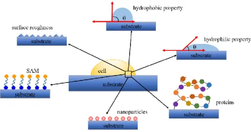
It has been repeatedly shown that the cell-substrate adhesion depends strongly on the physic-chemical properties of the material surface. The chemical composition at the surface represents an important factor for the surface energy, polarity, wettability, surface potential and as a consequence for the cell-substrate interaction [27] (Figure 2.2).
Figure 2.2: Schematic of differentphysic-chemical properties that have an influence on the cell-substrate interaction.
For example, the polar functional groups on the surface increase the energy, and wettability of the material, and support the adhesion and growth of cells on the surface [28]. If the surface is hydrophobic, the cell adhesion protein is adsorbed in a denatured configuration, thus specific amino acid sequences which should be working as ligands for adhesion receptors, will not or only partly be accessible. Then receptors cannot cluster into focal
2. Theoretical background and state of the art
adhesion plaques and associate with other structural and signaling proteins. Whereas, on moderate hydrophilic surfaces, proteins are adsorbed in a more natured and organized way.
The receptors then cluster into focal adhesion plaques and communicate with other focal adhesion proteins and the actin cytoskeleton [29, 30].
Various biomolecules [31] and nanoparticles [32] have been widely used in regulating cell- substrate adhesion. For example, in one study fibronectin patterns are designed with the structures of circles, squares, rectangles, pentagons and stars, and the cells are distributed on these structures [33]. Gold nanoparticles significantly increased the attractiveness of the polyethylene surface for the adhesion and growth of rat vascular smooth muscle cells [34].
Self-assembled monolayers (SAMs) are highly controllable in modifying surfaces and have been employed to mimic the ECM for cell-related studies. On self-assembled monolayers terminated with positively charged -NH2 groups, a much higher number and larger area of bovine aortic endothelial cells are obtained than on the negatively charged -COOH groups [35]. The negative charge seems to reduce the cell-material adhesion and also the cell-to- cell adhesion [36-38]. Sulfonate groups represent another typical example of negatively charged groups which suppress the cell adhesion. For example, they can be used for developing anticoagulant blood-contacting surfaces [39].
Another important factor for cell-substrate interaction is the roughness and topography of the surface. Generally, nanostructured substrates are considered to be beneficial for cell adhesion and growth. The reason is that nanostructures mimic the nano structure of natural ECM, for example nanofibers, nanocrystals or nanosized folds of ECM molecules. On nanostructured surfaces, ECM molecules can be adsorbed in the appropriate geometrical orientation which allows cell adhesion receptors to access to specific sites in the ECM [27].
However, cells typically spread incompletely on rougher surfaces since they can adopt an irregular, elongated shape, whereas the cells homogeneously covered on well-flattened smoother surfaces [40].
2.2.2 Engineering the cell-substrate interface towards guided growth
Patterned neuronal cells and guided neurite growth are important for applications such as prostheses, biosensors, and tissue engineering. Recently, technological advances allow us to precisely engineer the geometry and chemistry of substrate surfaces which enables the control of the cell interaction with the substrate or even the guided cell growth. These methods allow the production of substrate features on a nano and micron level.
Micropatterned surfaces allow a selective cell adhesion and guided growth, which can be used in tissue engineering, neuroelectronics and biosensors [27]. Nanopatterned surfaces
2. Theoretical background and state of the art
9
represent an effective method for controlling the spacing and distribution of ligands for cell adhesion receptors on surfaces [27]. Therefore, the cell proliferation, differentiation and other functions can also be manipulated. Some of the most commonly used surface engineering methods are microcontact printing, photolithography and electron beam lithography. In the following examples of different patterning methods are subdivided in two categories: starting with additive or bottom-up methods followed by subtractive or top- down methods.
Additive or bottom-up methods (Figure 2.3):
In additive or bottom-up methods target material or biomolecules are locally added onto the desired surface via either a stamp/probe contacting or a print head shooting drops. There are certain advantages of these methods. For instance, they are economic, productive, straightforward, local distributed and don’t require a harsh environment (cleanroom).
However, the disadvantages are also quite obvious. The resolution is not that high compared with the subjective methods (as shown later). An exception is obviously the scanning probe lithography (Figure 2.3c) which is very complex and definitely not suitable for mass production.
Figure 2.3: Examples of additive patterning techniques. (a) Micro- and nanocontact printing, SAM or proteins patterns are achieved by region-selectively transfer of a molecular ink onto the substrate using an elastomeric stamp. (b) Inkjet printing, ink drops of SAMs or proteins are dropped on to a substrate via a print head. (c) Scanning probe lithography, by using nanoscopic probe tips which locally add molecules. Adapted from [41].
2. Theoretical background and state of the art
(i) Micro- and nanocontact printing
Nanocontact printing which represents an extension of microcontact printing, is a highly parallel, manufactural, and additive process that allows printing of 100 nm structures. It uses a stiffer elastomeric stamp and high molecular weight inks to limit the diffusion and guarantee the spatial resolution. Typically, microstructured elastomer PDMS stamps are used to transfer the intended molecules onto substrates (Figure 2.3a). The straightforward stamp-dependent method also has limitations and disadvantages. For instance, in the sub- micrometer regime, the PDMS stamps can lose their mechanical integrity and deform which leads to an inherently limited spatial resolution [42].
(ii) Inkjet printing
The adaptation of ‘standard office printers’ for the deposition of bioinks leads to another additive technique. In this technique even individual neurons can be printed. These deposition devices are typically composed of commercial printer parts, i.e. ink reservoir, print head, and a movable substrate table (Figure 2.3b). Piezoelectric or thermal inkjet printers can be used to release a certain fluid volume onto the substrate. For example, PLL has been printed as an adhesive material bioink on polyethylene glycol (PEG) substrates showing a strict pattern of neurons over 25 days without any detriment of the electrophysiological properties or the synaptic distribution [43].
(iii) Scanning probe lithography
Scanning probe lithography techniques have a lot of advantages compared with other conventionally used fabrication techniques. Not only that it can create nano-size patterns but also it can be performed under ambient condition. For example, dip-pen nanolithography (DPN) utilizes functionalized atomic force microscope (AFM) tips to directly transfer molecules in the defined pattern on the substrate (Figure 2.3c). Different patterns are directly produced by coating tips with the biomolecules of interest typically in a humid chamber, this technique provides extremely flexibility in the fabrication of nanostructures.
Up to now, DPN has been already used for creating protein nanoarrays on nickel oxide, silicon oxide, and gold surfaces [44-46]. However, this technique still has its drawbacks.
For instance, the development of adequate inks, the stiffness of the tip and, last not least, this is a time-consuming process which doesn’t allow large area processing or mass production [47-49].
2. Theoretical background and state of the art
11
Subtractive or top-down methods (Figure 2.4):
In contrast to addictive or bottom up methods, the subtractive or top-down methods represent another way of constructing patterns. In these methods, normally a photo resist has to be prepared on the substrate beforehand. Then, depending on the unique properties of the photo resist, after exposed either to UV light or electron beams, the photo resist will crack and can be removed during development (or, alternatively, the photo resist will be polymerized, and the rest will be removed). This way the designed structure can be achieved. Although these methods are more complicated, they will lead to a high resolution, and allow large area and mass production.
Figure 2.4: Example of subtractive patterning techniques showing photolithograph (a), e- beam lithography (b) and a direct method, laser ablation (c), where a focused laser beam generates the surface topography. Adapted from [50, 51].
(i) Photolithography
As shown in Figure 2.4a, photolithography starts by coating the substrate with a photoresist.
Then, the resist is exposed to UV light through a mask with the desired pattern. At the exposed area the photoresist will be ‘cracked’, and in the final step is washed way using a developer solution.
Photolithography is a powerful technology for micropatterning. However, it requires the expensive clean room facilities and is limited to micrometer resolution. For most biological applications which only require micron level precision this is sufficient. Nevertheless, some experiments do require submicron resolution, which can be accomplished by e-beam
2. Theoretical background and state of the art
lithography.
(ii) Electron beam lithography
Electron-beam (e-beam) lithography (EBL) represents a maskless lithography method. It uses an electron gun similar to a scanning electron microscope. In contrast to photolithography, the resolution of EBL reaches a level down to a few nanometer. Similar to photolithography, the substrates are first coated with a resist which alters when exposed to the e-beam [52]. Similar to photolithography, EBL requires a cleanroom facility.
However, it is very flexible (patterns are programmed) and provides sub-micron resolution.
(iii) Laser patterning
Surface patterns can also be achieved directly, for example by pulsed laser ablation. In this process a high-intensity laser pulse is focused on a spot on the substrate where the absorbed electromagnetic radiation excites electrons and is converted into heat. If the energy is large enough material is removed by melting and vaporization (Figure 2.4c). Laser patterning can be employed for a wide range of materials like polymers, semiconductors, ceramics, or metals. This technique allows a submicrometer which largely depends on parameters of the laser beam such as laser wavelength, beam profile, pulse duration, physical properties of the sample material, and environmental gas pressure.
The main advantage of the direct writing technique lies in its flexibility, which allows to obtain arbitrary patterns and even morphologies in a single step and without a mask.
However the processing time depends on the resolution, sample size, and laser repetition rate and therefore is usually quite low. Unlike ion or electron beams, which represent alternative sources for the direct writing, laser surface patterning doesn’t require a vacuum or cleanroom. Moreover, it isn’t limited to planar substrates and relatively inexpensive [53].
2. Theoretical background and state of the art
13
2.3 Surface functionalization with organic SAMs
Figure 2.5: Schematic of the functionalization of a substrate with a SAM consisting of organic molecules (blue circle indicates the chemisorbing head group and orange circle functional group) which can be chosen with a variety of chemical functionalities. The green half circle represents the biological object (e.g. a cell), the interface between substrate and cell is modified by the molecular monolayer. Adapted from lab collection.
Self-assembled monolayers (SAM) are ordered molecular assemblies that form spontaneously with a specific affinity of their head groups to the substrate. Figure 2.5 shows a schematic, including the constituents of a SAM-molecule (head group, back bone, functional group). SAMs can be utilized in various technical applications, for example, protective coatings [54, 55], adhesion [56], building blocks in heterostructure and chemical anchors [57], surface chemistry, electronic properties [58], biointerface applications [59].
As shown in Figure 2.5, SAMs can behave as a link between organic cells and inorganic substrates, i.e. they are ideal for interfacing biological materials.
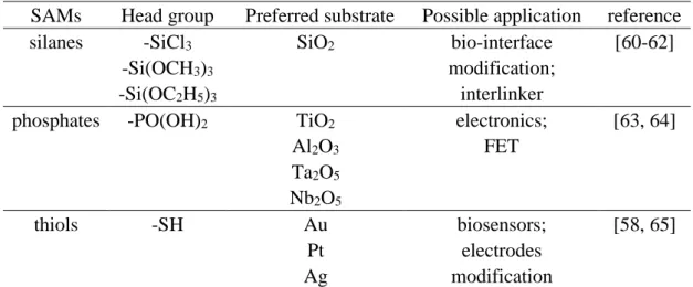
There are different types of organic SAMs with respect to their head group, such as thiols, silanes or phosphonates (Table 1). For sure the kinds of the different SAMs are far beyond the given examples in Table 1. It is also worth noting that each head group also has its preferable type of substrate, to which it binds.
2. Theoretical background and state of the art
Table 1: Examples of typical SAMs for different head groups and their corresponding substrates
SAMs Head group Preferred substrate Possible application reference silanes -SiCl3
-Si(OCH3)3
-Si(OC2H5)3
SiO2 bio-interface
modification;
interlinker
[60-62]
phosphates -PO(OH)2 TiO2 Al2O3
Ta2O5
Nb2O5
electronics;
FET
[63, 64]
thiols -SH Au
Pt Ag
biosensors;
electrodes modification
[58, 65]
In general, the self-assembling molecule consists of three parts: the head group, the back bone and the functional group. The head group is responsible for the anchoring of the molecule onto the substrate. Therefore, different head groups have their preferred substrates to which they bind. The alkyl (back bone) chain provides the stability of the molecular monolayer. Due to the van der Waals interactions between adjacent molecules, it also has a significant impact on the ordering of the SAM. Finally, the terminal end group provides the chemical functionality of the monolayer system and therefore it defines the overall property of surface. To a certain extent suitable molecules are commercially available or can be prepared by known chemical reactions.
2.3.1 Silane SAM on oxides
The typical process of SAM formation of silanes on SiO2 consists of two steps (Figure 2.6):
(i) Activation of the SiO2 surface which leads to a reconstruction of the silanol bonds at the surface,
(ii) Binding of silanes with their headgroups to the open silane groups.
Freshly prepared SiO2 possesses silanol groups on the surface. If the surface is exposed a humid environment, Si–OH undergoes a condensation reaction, forming the more stable siloxane group Si–O–Si. In this state, the Si surface possesses fewer open bonds and, as a result, the quality of a silanization would be poor. The activation, for instance, with an oxygen plasma leads to a recovery of the silanol groups and allows a dense coverage of the surface with silane molecules.
2. Theoretical background and state of the art
15
Figure 2.6: Schematic of the structure of SiO2, activation and binding of silanes.
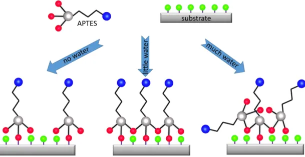
Role of water: It is known that the presence of water at the interface has a large impact on the reaction of the open silanol group therefore the water content is carefully controlled during the silanization. As shown in Figure 2.7, only without water or little water, there is a chance of forming a perfect monolayer, whereas excess water facilitates polymerization and the formation of thick polymer films. One way to avoid the problem of moisture is the use of a gas-phase deposition technology which allows a precise control of the deposition condition. This is one of the reasons, why we developed a gas-phase based deposition technique for the deposition of silane SAMs.
Figure 2.7: Schematic representation of the structure of silane layers for different water content. Adapted from [66].
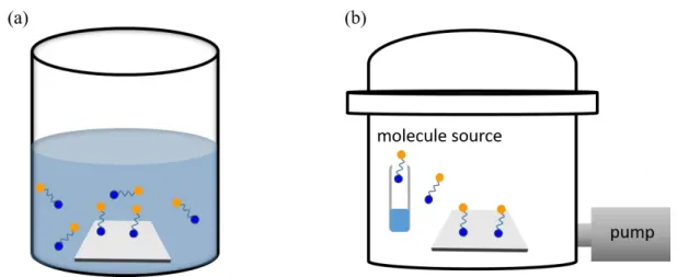
Liquid phase deposition (LPD):
The simplicity and the low costs are important reasons for the use of LPD for the deposition of organic molecules. In principle, the cleaned (and maybe activated) sample has to be submerged into a molecule solution for a certain time, and a molecular layer automatically assembles (Figure 2.8a). For silane-based systems, for example, the water content is extremely important for the proper preparation of the SAM. Additionally a proper outgassing of the solution is important and after completion of the SAM, an appropriate
2. Theoretical background and state of the art
rinsing procedure has to be applied. Therefore, although the process is simple, the resulting film quality and properties are often not reproducible.
Vapor phase deposition (VPD):
The principle of VPD can also be very simple. For this method substrate and molecular source are placed in a chamber. By evacuating the chamber, molecules are evaporated onto the substrate (Figure 2.8b). The molecular source can be heated moderately to increase the vapor pressure of the molecules. While employing a vacuum chamber generally is more expensive, the advantages of VPD over LPD are in the protection of the environment, the better control of the process, and last but not the least, the avoidance of moisture. These are the reasons why we choose VPD in this work.
Figure 2.8: Schematic of LPD and VPD routes of the deposition of molecular SAMs.
Silanes on other oxides: As discussed above, the adhesion of silanes on SiO2 involves condensation reactions between the hydroxyl groups of the SiO2 substrate and the silane.
Therefore the concentration of the Si-OH groups on the surface is an important parameter to optimize the SAM’s quality. A classification of adhesiveness of organosilanes on various inorganic substrates is given in Figure 2.9. Aluminum (Al2O3) has a better adhesion compared with other inorganic oxides [67, 68], but all of them show a worse adhesion behavior compared with SiO2. This difference in adhesiveness results mainly from the different structures of the oxides and the resulting concentration of hydroxyl bonds.
2. Theoretical background and state of the art
17
Figure 2.9: Binding effectiveness of silanes on different inorganic oxides, taken from [68].
2.3.2 The role of the functional group
As indicated in Figure 2.5, the interface between the object (here a cell) and substrate has been functionalized by a SAM. The new interface is determined by the property of the functional group of the SAM. Since we are working with silanes, their head groups have similar chemical properties, which allow to bind to SiO2 surface. However, silanes can differ in the length of the backbone and the choice of the functional group. Table 2 lists similar silanes with commonly used functional groups.
2. Theoretical background and state of the art
Table 2: Examples of silanes with different functional groups and their applications.
Functional group
examples application property references trifluorometh
yl/trimethyl -(CF3)/(CH3)
propyltriethoxysilane(
CH3(CH2)2Si(OC2H5)3
);
trichloro(3,3,3- trifluoropropyl)silane (C3H4Cl3F3Si)
stamp fabrication;
hydrophobic modification;
friction control in micro machines
hydrophobic [69, 70]
amino -NH2
3-
aminopropyltriethoxy silane (APTES) N-(2-aminoethyl)-3- aminopropyltrimethox ysilane (EDA)
(3-
trimethoxysilylpropyl) diethylenetriamine (DETA).
immobilization of biomolecules;
cells adhesion
protonated at pH7.4
[71-74]
thiol -SH
(3-
mercaptopropyl)trimet hoxysilane (MPTS)
metal nanoparticles bond to metal [75]
epoxy -C2H3O
(3-
Glycidyloxypropyl)tri methoxysilane (GLYMO)
immobilization of biomolecules;
bio incompatibale interface
very reactive [76]
As shown in Table 2, there are different functional groups which can be chosen to modify the substrate’s surface and achieve the desired properties. For example, -CF3/CH3 is often used in stamps fabrication due to its excellent hydrophobic properties. -SH groups can be used to link gold nanoparticles. Epoxy groups are very reactive and can be used to immobilize biomolecules.
In our case we wanted a SAM that is suitable for guided cell growth. It is known that proteins on the cell membrane have negative charges. Therefore, in order to make the surface attractive for cells, the surface should be positively charged. The amino group (- NH2) can fulfill this task, since it becomes positively charged in an electrolyte. Therefore, it might be a good candidate for the functionalization of a “bio-unfriendly” surface and turns it into a biocompatible surface.
2. Theoretical background and state of the art
19
2.4 Electronic cell-chip coupling
A central goal of neuroelectronics is the understanding of the functional connectivity of neuronal circuits, for example, to learn more about their physiological functions.
Nowadays, the available methods for the recording of neural activity include [77]:
(i) Intracellular recording and stimulation using either sharp or patch electrodes, (ii) Extracellular recording and stimulation using substrate-integrated
microelectrodes or microelectrode arrays (MEAs),
(iii) Magnetic resonance imaging (MRI), electroencephalography (EEG) and magnetoencephalography (MEG), which allows to record activities of large-scale neural populations and therefore isn’t suitable for single-neuron resolution.
The advantage of intracellular recording systems is that they exhibit very large signals and provide accurate readouts of the entire dynamic voltages range of the cells during the measurement. However, the use of sharp or patch microelectrodes is first of all limited to individual neurons and, second, it is not suitable for a long-term and multiple network measurement. Furthermore, the neurons will die during or shortly after the measurement.
In contrast, the non-invasive extracellular MEAs enable the simultaneous recording and stimulation of a larger population of cells, and for a period of days and months without or little damage to the neuron’s membrane [78, 79]. However, in order to achieve a good signal-to-noise ratio of recording as well as allowing stimulation of cells, it is of vital importance to achieve a good cell-chip coupling. If we neglect the relatively high conductance of the electrolyte, the cell-chip coupling is determined by two factors (Figure 2.10):
(i) interfaces, namely the cell-electrolyte interface and the electrode-electrolyte interface, and
(ii) the sealing resistance Rseal, defined by the cleft.
These interfaces’ impedance can be represented by the parallel arrangement of a resistor and a capacitor (Figure 2.10). Whereas the cell-electrolyte interface is determined by the cells and medium, we can only affect the second interface, i.e. the electrode-electrolyte interface, by modifying the surface of the electrode.
The leakage current is mainly defined by the size of the cleft. The smaller the cleft, the larger is the leakage resistance Rs and the smaller is the loss of signal transfer. Since the cleft size strongly depends of the cell adhesion, this aspect is in principle already discussed in the previous sections.
2. Theoretical background and state of the art
Figure 2.10: Schematic of a neuron on a substrate-integrated planar electrode as well as the corresponding analogue electrical circuit. The neuroelectronic hybrid consists of a neuron, a cleft between neuron and substrate, and an electrode.
The structural relationship between a neuron and a substrate-integrated planar electrode and the corresponding electrical circuit is shown in Figure 2.10. The neuroelectronic interface is composed of three components, a neuron, a cleft between the neuron and the substrate surface, and an electrode. For the simplified model shown in Figure 2.10, the neuron surface can be further divided into a junctional membrane which faces the sensing pads (with Rj and Cj as the junctional resistance and junctional capacitance, respectively), and the non-junctional membrane (with Rnj and Cnj) which faces the culture medium. The cleft, between neuron and electrode causes an electrode-electrolyte impedance (with Re and Ce) and a resistance, called seal resistance (Rseal) [80].
2.4.1 Action potential and cell-electrolyte interface
The action potential (AP) represents an electronic pulse during which the cell’s membrane potential quickly raises and falls. Such APs can propagate through cellular layers and are responsible for a large variety of organism functions like sensing, thinking, moving and heart beating.
2. Theoretical background and state of the art
21
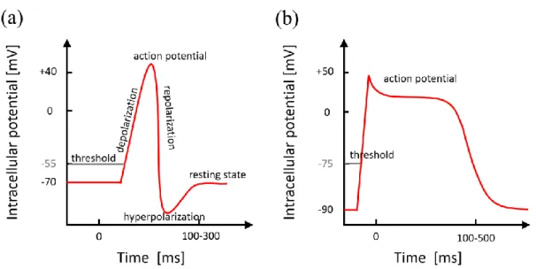
Figure 2.11: schematic of action potentials of a neuronal cell (a) and a cardiac muscle cell (b). The action potential duration of a neuronal cell is short (<5 ms), compared with the duration of HL-1cell lasts tens of ms with a long repolarization period of up to 200ms.
Adapted from [81-84].
Typical neuronal and cardiac APs are shown in Figure 2.11. In equilibrium, the cells are at resting potential, which is usually around -70 mV for neuronal cells and -90 mV for cardiac muscle cells. An electronic stimulation can temporarily depolarize the membrane. If the stimulation is not strong to reach the threshold of -50 ± 5 mV or -75 mV for neuronal cells and cardiac muscle cells respectively, the action potential will not be fired. Otherwise if depolarization potential reaches the threshold value, the protein channels in the membrane which control the sodium will open and sodium ions (Na+) flow into the cell due to the chemical gradient. The concentration of Na+ is enhanced in neuronal and cardiac cells which will increase the membrane potential to +40 ± 10 mV. While the accumulation of Na+ in the cell, there are too much positive ions, therefore the potassium ions (K+) channel will open and K+ leaves the cell. The efflux of K+ is the reason that results in a membrane hyperpolarization, the membrane potential can reach even values lower than the resting potential. The principle of a cardiac muscle AP is very similar (Figure 2.11b), the first repolarization step is caused by the potassium efflux that is the same with neuronal cells (Figure 2.11b), however, there is a characteristic plateau caused by the impact of slow Ca2+
channels, keeping the membrane potential at a high potential for around 200 ms. The final repolarization is due to the ongoing efflux of K+ ions [81-84].
The cell-electrolyte interface is in principle defined by the membrane of the cell which is made of bilayer phospholipid molecules. The membrane has an approximate thickness of 5 nm, and in general it represents a perfect insulator. However, in the case of electro active cells such as neurons or cardiac muscle, the membrane incorporates ion selective channels
2. Theoretical background and state of the art
and pumps, allowing ions to flow in and out of the cell’s cytosol. There is a variety of factors which can affect the ion channel’s conductivity, and therefore can cause the changes in the ionic concentration, and consequently lead to depolarization and repolarization of the membrane [81].
2.4.2 Electrode-electrolyte interface
As discussed above, the cell-electrolyte interface heavily depends on the medium that the cells are placed in. Therefore there is little we can do to modify this interface and its properties. However, the electrode-electrolyte interface can be manipulated, for instance, to achieve a high signal recording. One can:
(i) introduce a better mechanical coupling (see sections above) and, thus, a smaller cleft, which in the end leads to smaller signal losses, or
(ii) modify the electrode-electrolyte interface by modification of the interface and, thus, reduce the electrode-electrolyte impedance.
Our option is the functionalization of the surface with organic molecules, which could affect not only the cleft size but also the impedance of the interface.
Sealing resistance:
It is obvious that the amplitude and shape of the recorded AP signal depend on Rseal. Studies of the cell-electrode interface show typical cleft size between 40-100nm [7, 85-87]. For most cell types this corresponds to an Rseal value of the order of 1-2MΩ and APs recordings of 10-100 mV [80].
Electrode-electrolyte impedance:
Another component which affects the electronic coupling of cells and electrodes is the input impedance Ze of the electrode. The type of charge transfer of a living cell and an electronic device are fundamentally different, i.e. the former is formed by ion transport and motion in a solution whereas the latter is given by electron motion in metals [88, 89]. Due to this difference the electronic coupling is represented by an impedance. Typically the impedance of the sensing electrode is attributed to the ‘blocking’ ion bilayer, Helmholtz layer (Figure 2.12) which forms on any surface in an ionic solution. Reducing the surface area of an individual electrode to match the dimensions of individual neurons allows a local measurement of neuronal signal and, in case of the use of MEAs, an increase of the spatial resolution [90-92]. However, this automatically reduces the amplitudes of the recorded signal and consequently reduces the signal-to-noise ratio. Therefore, the electrode’s
2. Theoretical background and state of the art
23
geometry and the resulting impedance lead to constraints on the electrode size. Typical approaches to increase the surface area are nanostructures, for instance spongy platinum black or Ti3N4 [93], gold nanoflakes and nanopillars [94, 95], or carbon nanotubes [96].
According to our group’s research, using organic molecules to functionalize the metal surface could also affect not only the cleft size but also the impedance of the interface. This will not be discussed in this work.
Helmholtz or electrical double layer: If a solid (insulator, semiconductor, metal) particularly an electrode, is placed into an electrolyte, an electronic interface develops in form of an electrical double layer (EDL). The EDL is an ionic arrangement at and near the surface (Figure 2.12). Its first layer is typically a layer of water molecules, especially adsorbed on the surface, while the second layer is composed of the oppositely charged hydrated ions, attracted by the Coulomb force. These ions partially screen the charge of the object. The second layer cannot be considered static, but rather diffusive.
Helmholtz firstly proposed the double layer theory that the EDL can be described as a parallel-plate capacitor [97]:
C = ε0𝜀𝑟𝐴
𝑑 (1)
where ε0 represents the dielectric constant of vacuum, εr indicates the relative dielectric permittivity of the solvent, A is the area of the electrode and d is the distance between the electrodes.
L.G. Gouy and D.L. Chapman observed that the EDL capacitance is not constant but frequency dependent. Therefore, they developed the Helmholtz model further by considering the thermal movement of the ions and proposed a diffuse layer of ions at the charged surface. According to this model local, the ion concentration depends on the potential Φ at a distance d from a surface with a potential Φ0 [98-99]:
Φ = Φ0× exp(−𝑑
𝜆𝐷) (2) with the Debye length λD given by [100]
λ𝐷 = √ε2𝑛0𝜀𝑟𝑘𝐵𝑇
0𝑧2𝑒02 (3)
where n0 is the bulk concentration of ions in the electrolyte, e0 is the elementary charge, z is the ion charge, kB is the Boltzmann constant, and T is the temperature.
The excess charge at the solution side is electrostatically attracted to the electrode interface, but this attraction is counteracted by the random thermal motion which aims to equalize the concentration in the solution. The overall equilibrium can be computed via the linear
2. Theoretical background and state of the art
Poisson-Boltzmann equation [101]:
𝑑
2𝛷
𝑑𝑥2 = 𝛷(𝑥)
𝜆𝐷2 (4)
Solving the simplified Poisson-Boltzmann equation results in the Gouy-Chapman capacity [81]:
C𝐺𝐶 = ε0𝜀𝑟
λ𝐷 cosh(𝑧𝑒0𝛷(0)
2𝑘𝐵𝑇 ) (5)
The Gouy-Chapman model considers all ions as point charges, which can approach the surface infinitely close. This assumption leads to a major drawback of an unlimited increase of capacitance at high ionic concentrations. This has never been verified experimentally, therefore the model was further improved by Stern in 1924.
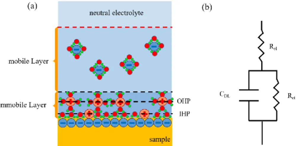
Stern stated [102] that ions cannot approach the electrode’s surface closer than their ionic radius. The distance of the closest possible approach is called Outer Helmholtz Plane (OHP). The ion distribution of the OHP can be considered as a cloud of ions with a higher concentration at the electrode which decays away from the electrode surface. The ion cloud is called the Gouy-Chapman diffuse charge layer (GCL). Some ions even penetrate the hydration sheath and adhere to the electrode. The plane in front of the electrode surface is defined by a layer of absorbed water molecule, the Inner Helmholtz Plane (IHP) (Figure 2.12a).
The properties of the space-charge distribution is shown in Figure 2.12a and can be summarized by an equivalent electric circuit (Figure 2.12b) consisting of an electrolyte resistor Rel in series with the parallel connected of a charge transfer resistor Rct and EDL capacitor CDL.
Figure 2.12: Electrode-electrolyte interface and equivalent electrical circuits. (a) Schematic representation of an electrode-electrolyte interface, (b) electrical circuit of the electrode-electrolyte interface.
2. Theoretical background and state of the art
25
The discussions above are based on bare electrode-electrolyte interfaces. In our work, we used SAMs of organic molecules to functionalize the surface of our substrate. It can be expected that this functionalization not only affects the mechanical cell-substrate interaction with all its consequences on the sealing resistance and the growth behavior, it can also directly affect the EDL and thus the electrode-electrolyte impedance. We therefore expect that the SAM might have an impact on the mechanical and electronic cell-chip coupling.
3. Sample preparation, characterization and experimental techniques
3. Sample preparation, characterization and experimental techniques
In this work, we applied a series of experimental techniques ranging from deposition, lithography, characterization, cell culture to electronic measurements. The techniques listed and sketched in this chapter are:
(i) Various deposition techniques, which include molecule layer deposition (MLD), atomic layer deposition (ALD) and metal evaporation.
(ii) Electron beam lithography including pattern design, lithography, etching and lift- off technique.
(iii) Characterization methods such as ellipsometry, contact angle measurement, and streaming potential measurements.
(iv) Cell culture experiments including cortical rat neurons and HL-1 cell cultures, as well as staining experiments and critical point drying.
(v) Electronic characterization methods to analyze different types of MEAs and cell chip communication.
3.1 Deposition techniques
There exists a larger number of techniques for the deposition of thin films. In this work only gas phase based technologies (VPD) are used. The deposition of organic layers is done by molecule layer deposition (MLD) and the different oxides thin films are deposited via atomic layer deposition (ALD). Furthermore, electron beam evaporation is used for the production of metal layers (i.e. electrodes).
3.1.1 Molecule layer deposition
Figure 3.1 shows the image and a schematic of the MLD device used in this study. It allowed us to perform all important deposition steps including surface activation via ozone, subsequent molecular deposition from the gas phase, and post-deposition treatment without breaking the vacuum. The different components of the MLD setup (Figure 3.1) are:
Deposition chamber, where the samples and sensors (e.g. capacitive sensor or surface acoustic wave (SAW) sensor) are placed for the activation and deposition process.
Ozone generator, which converts O2 to O3 (ozone) for cleaning and activation of the surface.
Molecule source, which contains the molecules, and valves for the deposition.
3. Sample preparation, characterization and experimental techniques
27
Pumps and gas sources (O2, Ar, N2) to keep the constant pressure of a given gas (alternatively vacuum) during deposition and post-deposition treatment.
The different process steps necessary for the deposition of molecule layers are explained in the following.
Figure 3.1: (a) Image and schematic of the MLD setup, which shows (from left to right) the Ar gas supply (blue) for the working gas used during the deposition, the molecule source (yellow and green), the main chamber (yellow) including the in situ capacitive or SAW sensor – where activation and deposition takes place – and the microwave oven (blue) producing ozone (purple) for cleaning and activation of the samples and sensor. All essential ingredients are separated via valves (red) from the recipient, which is pumped with a turbo pump and an oil-free forepump. Figure adapted from [103].
Activation and cleaning: First, thesubstrates were placed in the MLD chamber, which was then evacuated to ~10-5 hPa and flooded with oxygen (99.99% purity and a flow rate of 93 sccm), setting a pressure of 1 hPa via downstream control. Oxygen is activated and converted to ozone via a microwave discharge (2.45 GHz, 700 W), which then flows with the oxygen stream to the substrate. At the substrate, the ozone, first of all, removes organic residues from the surfaces of the substrate and recipient (cleaning) and second, can activate the surface. For example in case of Si/SiO2 substrate, the SiO2 surface forms open silanol
3. Sample preparation, characterization and experimental techniques
surface bonds (Si-OH) upon exposure to ozone, which are later used for the bonding of silanes (Figure 3.2).
Figure 3.2: Sketch of ozone activation leading to the formation of hydroxyl groups on a SiO2 surface [104].
Deposition process: After surface cleaning and activation, the oxygen supply was turned off and the process gas (Ar) switched on. We used an Ar flow of 27 sccm and established a process pressure of 0.1 hPa. The actual deposition of APTES was initiated by opening the valve of the molecular source. After 10 minutes of deposition, the valve was closed and the actual deposition terminated, see Figure 3.3.
Figure 3.3: Schematic of the deposition process. During the deposition process, an Ar flow is established at a typical process pressure of 0.1 hPa. The actual deposition of APTES is initiated by opening the source for the given deposition time of typically 10 min.
Post-deposition treatment (PDT): In this work, we noticed that a PDT is of vital importance to achieve an integrated self-assembled monolayer via vapor phase deposition. After the actual deposition, the samples could be removed directly (no PDT, i.e. tPDT = 0), or they can be kept in the MLD device for a PDT. During the PDT the Ar supply was switched off leaving the sample at a background pressure of ~10-5 hPa for a given time. The duration tPDT of this treatment was varied from 0 to 5 days. Although a higher temperature during PDT might accelerate SAM formation, the chosen conditions allowed us to observe the formation process in detail, as demonstrated in chapter 4.1.
3. Sample preparation, characterization and experimental techniques
29
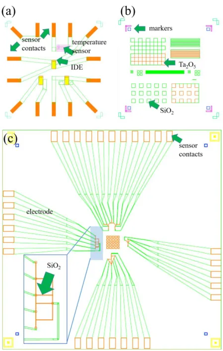
Capacitive sensor: Different in situ sensors have been developed for the analysis and control of the MLD process. We used a capacitive sensor with has been developed in a previous study [105]. This capacitive sensor is based on planar interdigitated electrodes (IDE) (Figure 3.4) that allow the recording of the dielectric permittivity of the molecular layer throughout the entire deposition process. The IDEs of the capacitor consists of a combination of a Ti (5 nm) and a Pt (10 nm) layer and form a capacitor (gap size s = 1 µm and effective length l = 10.8 mm) (lab protocol).
Figure 3.4: (a) Schematic of the interdigitated structure of the capacitive sensor, and example of the change of the (b) capacitive signal during the deposition of a molecular layer. Figure adapted from [105].
Since the total sensor capacitance Ctotal is given by the sum of the different contributions:
𝐶𝑡𝑜𝑡𝑎𝑙 = 𝐶𝑔𝑎𝑠+ 𝐶𝑠𝑢𝑏+ 𝐶𝑚𝑜𝑙 = 𝐶𝑟𝑒𝑓+ 𝐶𝑚𝑜𝑙 (6)
arising from the reference (gas, substrate), and molecular layer. The change of the capacitance during deposition indicates the contribution from the molecular layer:
𝐶𝑚𝑜𝑙 = 𝐶𝑡𝑜𝑡𝑎𝑙− 𝐶𝑟𝑒𝑓 (7)
An example of the resulting change of the signal during deposition and PDT is shown in Figure 3.4b.
3.1.2 Atomic layer deposition
In ALD processes, precursors (i.e. organic molecules) containing the atoms to be deposited are individually introduced into the deposition chamber in a sequence and react with the surface or molecule on the surface. After a complete cycle, the remaining molecules that are not reacting with the surface will be pumped out. This leads to a film deposition in a layer-by-layer method. ALD offers a great potential for the production of thin, pinhole-free films with a high control of the thickness and composition of the films at the atomic level.
![Figure 2.1: Schematic of the different phases of cell-substrate adhesion, adapted from [21]](https://thumb-eu.123doks.com/thumbv2/1library_info/3698183.1505897/14.892.218.712.416.630/figure-schematic-different-phases-cell-substrate-adhesion-adapted.webp)
![Figure 2.9: Binding effectiveness of silanes on different inorganic oxides, taken from [68]](https://thumb-eu.123doks.com/thumbv2/1library_info/3698183.1505897/25.892.226.694.111.686/figure-binding-effectiveness-silanes-different-inorganic-oxides-taken.webp)
![Figure 3.8: A schematic sketch of the different steps of the photolithography [101].Note that the objects (e.g](https://thumb-eu.123doks.com/thumbv2/1library_info/3698183.1505897/42.892.290.625.117.525/figure-schematic-sketch-different-steps-photolithography-note-objects.webp)
