Lecture 1: Design, Simulation and Test of a Combinational Circuit
G. Kemnitz
∗, TU Clausthal, Institute of Computer Science May 25, 2011
Abstract
A combinatorial circuit of a few gates will be simulated, described for synthesis, synthesized and loaded in a programmable logical circuit. The educational object is to become familiar with the different kinds descriptions and tools in the design process of combinatorial circuits.
1 Preparation
Download the achieve »PrVHDL-A1.zip« in the working directory of the laboratory course. Then unpack:
unzip PrVHDL-A1.zip
The archive contains the following files:
Aufg1/Sim_GHDL/Exor2_Sim.vhdl # description for simulation Aufg1/Sim_GHDL/Exor2_Synth.vhdl # description for synthesis Aufg1/Sim_GHDL/Test_Exor2.vhdl # testbench
Aufg1/Sim_GHDL/Test_Exor2.sav # visualization parameters for GTKWAVE Aufg1/Sim_GHDL/Exor2.sh # batch file for simulation
Aufg1/Exor2/Exor2.xise # project file for ISE Aufg1/Exor2/Exor2.ucf # constraint file for ISE
2 Simulation with GHDL and GTKWAVE
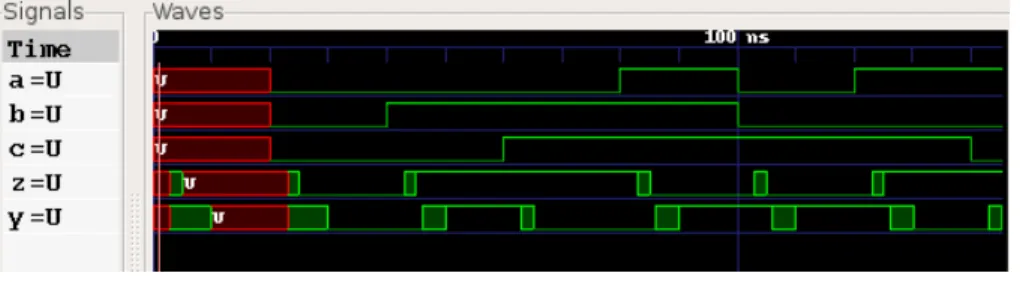
The example is the following circuit with two EXOR gates, described with hold and delay times:
td= 5 ns th= 3 ns
=1 z =1
c y ab
th,td th,td
The description consists of two concurrent signal assignments, which invalidate the signal at the right side of the assign operator »<=« after the hold time and assign a new valid value after the delay time:
z <= ’X’
after3 ns, a
xorb
after5 ns;
y <= ’X’
after3 ns, z
xorc
after5 ns;
∗Tel. 05323/727116
The complete description is in the file »Aufg1/Sim_GHDL/Exor2_Sim.vhdl«. In addition the simulation needs the testbench »Aufg1/Sim_GHDL/Test_Exor2.vhdl«, instantiate the device under test (DUT) and creating the input signals:
DUT:
entitywork.Exor2
port map(a=>x(0), b=>x(1), c=>x(2));Test:
process beginwait for
20 ns; x <= "000";
wait for20 ns; x <= "010";
wait for
20 ns; x <= "110";
wait for20 ns; x <= "111";
wait for
20 ns; x <= "100";
wait for20 ns; x <= "101";
wait for
20 ns; x <= "001";
wait;end process;
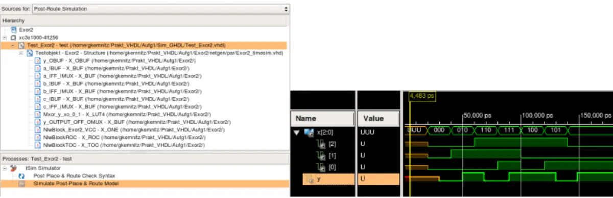
The instance of the device under test has no architecture name. This is a precondition to use the same testbench later in the design process in »ISE« for post-route simulation
1. The test process assigns always after 20 ns a new value to the input signal and stops simulation with the last wait statement after collectively 140 ns simulation time. Simulation under Linux:
• Menu »Anwendungen« . »Zubehör« . »Terminal« starts a terminal,
• change to directory » Aufg1/Sim_GHDL « cd Aufg1/Sim_GHDL
• execute the commands in the shell script »Exor2.sh:
ghdl -a EXOR2_Sim.vhdl # analyze DUT description
ghdl -a Test_Exor2.vhdl # analyze test bench
ghdl -m Test_Exor2 # make (produce the executable)
ghdl -r Test_Exor2 --wave=Test_Exor2.ghw # run simulation gtkwave Test_Exor2.ghw Test_Exor2.sav # visualize wave form
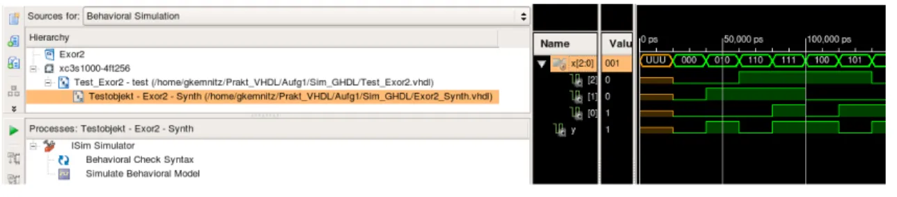
After starting GTKWAVE select via the menus and icons of the waveform viewer the signals and the time interval to be displayed. Figure 1 shows the waveform with the adjustments in the file
» Aufg1/Sim_GHDL/Test_Exor2.sav «.
Figure 1: Simulation result
Instead of typing in the single commands by the keyboard they also can be copied into the terminal with »Strg-C« and »Strg-V« or executed by running the shell script:
./Exor2.sh
1An instance without architecture name instantiate the last analyzed architecture to the entity in the library.
2.1 Circuit design with ISE
For synthesis the target function has to be described without invalidation of signal values, without printing text messages and without hold and delay times. Both signal assignments must be simplified to:
z <= a
xorb;
y <= z
xorc;
(see synthesis description »Aufg1/Sim_GHDL/Exor2_Synth.vhdl«). To simulate the simplified behavioral description in the shell script »Exor2.sh« the file name »Exor2_Sim.vhdl« has to be changed to »Exor2_Synth.vhdl.
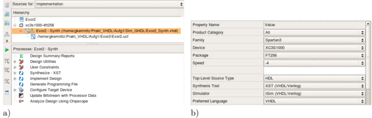
Start »ISE«
• menu: »Anwendungen« . »Umgebung« . »Xilinx ISE 11«
In the opening project navigator
• »File« . »Open Project«
• change to directory: »Aufg1/Exor2« and
• select the file »Exor2.xise«.
In the window »Sources for Implementation« should be displayed the programmable logic circuit
»xc3s1000-4ft256«, the file with the simulation description »../Sim_GHDL/Exor2_Synth.vhdl«
and the constraint file as in figure 2 a. In the process window below for the selected design object all possible operations are displayed. For the synthesize description in the figure these are e.g. syn- thesis, implementation and generate programming file. A double click on the programmable circuit opens the menu shown in figure 2 b. In this menu subsequently another type of programmable circuit, another simulator etc. can be selected. In this and in the following laboratory exercises the values must be those shown in the figure
2.
a) b)
Figure 2: a) Design sources for implementation and available operations b) Project parameters In the first step, the register transfer synthesis should be performed:
• select the description for synthesis »Exor2_Synth.vhdl« and
• click on »Synthesize - XST« . »View RTL Schematic«
After opening and an appropriate zoom the synthesized circuit in figure 3 will be displayed, an EXOR with three inputs.
2The adjustments are stored in the project file »Exor2.xise«.
Figure 3: Result of the register transfer synthesis
The next step after synthesis is the technology mapping. Start the process
• »Synthesize - XST« . »View Technology Schematic«
Our example circuit will be mapped to a single look-up table
3. At all connectors buffers for signal transformation are included. With a click at the look-up table the table contents is displayed as shown in figure 4 below right.
Figure 4: Circuit after technology mapping and contents of the look-up table
For placement and routing the project in addition needs an user constraint file. The constraint file contains the assignment of the circuit connectors to circuit pins and other additional infor- mation for synthesis, placement and routing. To edit the constraint file select it in the window
»Sources for Implementation«
4and start in the process window »User Constraints« . »Edit Constraints (Text)«. The lines in the given constraint file
NET "a" loc="F12"; # switch SW0 NET "b" loc="G12"; # switch SW1 NET "c" loc="H14"; # switch SW2 NET "y" loc="K12"; # LED LD0
3In our programmable logic circuit combinatorial circuits are mainly mapped to look-up tables with four inputs and one output. For a function with three inputs one of the inputs remains unused.
4no double click!
describe that input »a« should be connected to the package pin »F12« etc. The names of the package pins can be found beside the switches and LEDs on Spartan3 board used for testing. To generate the programming file the synthesis description has to be selected. Then
• start »Generate Programming File«.
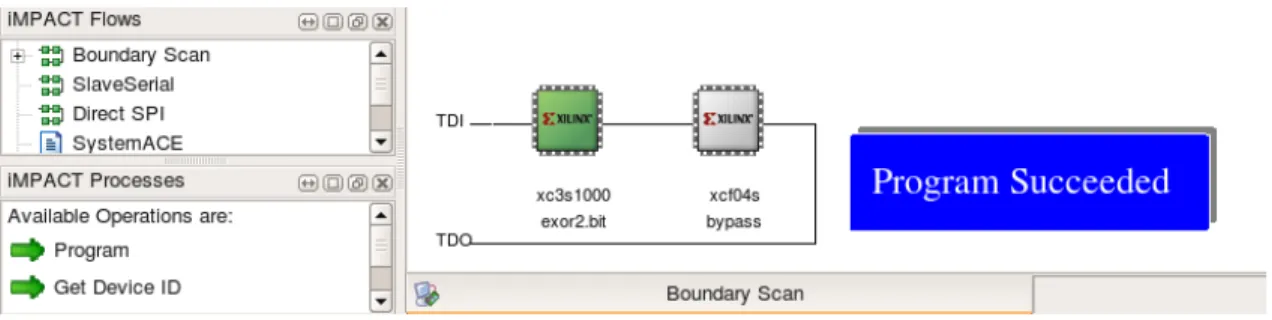
To program the programmable logic circuit start
• »Configure Target Device« . »Manage Configuration Project (IMPACT)«
IMPACT is a stand alone program. Programming needs the following steps:
• connect power supply and the programming cable to the board,
• in IMPACT start »File« . »New Project«,
• answer »yes« to »Do you want the system automatically ...«,
• in the next window select »Configure device using Boundary Scan« and »Automatically connect ...«,
• in the next window select»... assign configuration file(s)«,
• assign to the programmable logic circuit »xc3s1000« the file »Aufg1/Exor2.bit,
• leave to the flash memory »bypass« and
• close the next window.
After programming the IMPACT window should look as shown in figure 5. Boundary-Scan is a serial test and configuration bus with the signals TDI (test data in), TDO (test data out), TCK (test clock) and TMS (test mode select, see test connector at the board). Multiple circuits on a board form a chain. Each circuit type has a vendor and identification number which can be read by
• »Get Device ID«
in the window »IMPACT Processes«. Programming is to be performed in the same window with
• »Program«
After Programming, as shown in figure 5, the message »Program Succeeded« should be displayed.
After programming successfully the circuit is ready for testing.
Figure 5: Boundary-scan chain and assignments to both devices
2.2 Test
To test the example circuit consisting of two EXOR gates all combinations of switching values should be set and the the output has to be checked. The output LED should only be on, if the number of input switches, witch are on, is even.
2.3 Editing Placement
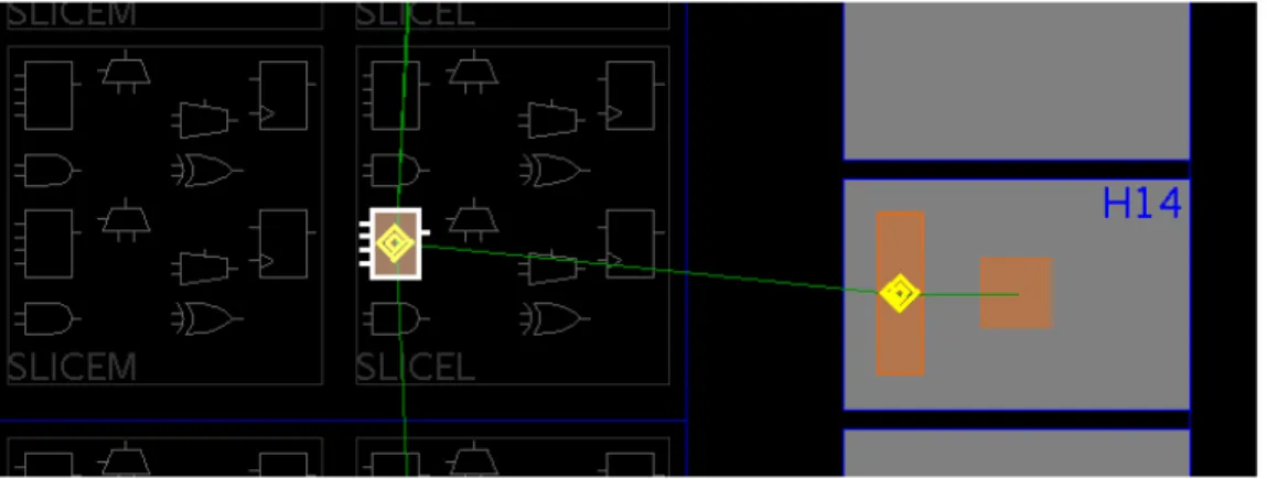
Usually, place and route is performed automatically. If required, placement can be corrected by hand before the generation of the programming file by starting »Implement Design«→ »Analyze Timing / Floorplan Design (PlanAhead)«. The program surface of »Plan Ahead« can besides oth- ers display a geometrical plan of all programmable parts of the programmable circuit. Our circuit has 1.920 programmable logic blocks, 24 configurable block RAMs, 24 multipliers, 4 configurable clock generation devices and 391 programmable input/output circuits. With a strong zoom it shows that all programmable logic block consist of four slices and each slice of two programmable look-up tables with four inputs and one output, two flip-flops and some additional special purpose gates and multiplexers
5. Figure 6 shows a small part with the look-up table of the example circuit and the driver for input »c«. In the computer generated layout the look-up table is arranged in a way that distances to each connector are minimal. For the screen shoot it has been moved by the mouse. In this way each sub-circuit can be rearranged.
Figure 6: Placement with PlanAhead
2.4 Run time analysis
With »Implement Design«→ »Generate Post Place and Route Static Timing« → »Analyze Post- Place & Route Static Timing« the maximum delay times between all connectors through the circuit are calculated and displayed:
All values displayed in nanoseconds (ns) ---+---+---+
Source Pad |Destination Pad| Delay | ---+---+---+
a |y | 10.073|
b |y | 10.084|
c |y | 8.615|
---+---+---+
The cause of the smaller delay time from input »c« to the output is the replacement of the look-up table close to input »c« in figure 6.
5e.g. for fast carry propagation