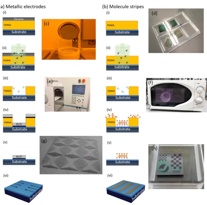
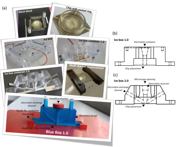
Molecular Layer Functionalized Neuroelectronic Interfaces:
132
0
0
Volltext
(2)(3)
(4)(5)
(6)
(7)
(8)
(9)
(10)
(11)
(12)
(14)
(15)
(16)
(17)
(18)
(19)
(20)
(21)
(22)
(23)
(24)
(25)
(26)
(27)
(28)
(29)
(30)
(31)
(32)
(33)
Abbildung
+7
ÄHNLICHE DOKUMENTE
Der praktisch niedrig positionierte Objekttisch für eine opti- mierte Körperhaltung des Betrachters und leichten Zugang hat eine neue, hartbeschichtete Oberfläche, die sich leicht
In a grave in Kotchari, two clay models, about 19 cm and 23 cm high, were found which consist of a rectangular panel, in which three pillars are embedded which are topped by
Comparison of SEM images of carbon nanotube films on platinum substrates prior and after cell culture experiments with NIH3T3 fibroblastes: Bayer MWNTs, Fraunhofer SWNTs, SWeNT
Extending our previous work on determining the two-particle-structure factor from inelastic diffractograms, we now compare simulations of amorphous structures with
An additional benefit for polymer imaging is that helium ions scatter mainly from the nuclei of the target and do not interact with the chemical bonds directly – this makes it
For the monetization of the impact category freshwater ecotoxicity regarding the MMG method and Environmental prices, for example, the valuation of the AoPs was known and suggested
The thesis takes into account three articles about famous persons from Serbia, Bosnia and Herzegovina, Croatia, and Slovenia, across different Wikipedia language versions –
We argue that molecules are deposited as dimers that undergo, upon increase of temperature, a series of structural transitions from clusters to ordered striped and then dense
