SiMPl—Novel high QE photosensor
Jelena Ninkovic´
a,d,, Ladislav Andricˇek
a,d, Gerhard Liemann
a,d, Gerhard Lutz
c, Hans-Gu¨nther Moser
a,d, Rainer Richter
a,d, Florian Schopper
b,daMax-Planck-Institut fu¨r Physik, Fo¨hringer Ring 6, D-80805 Munich, Germany
bMax-Planck-Institut fu¨r extraterrestrische Physik, Giessenbachstraße, D-85748 Garching, Germany
cPNSensor GmbH, Ro¨merstr. 28, D-80803 Munich, Germany
dMax-Planck-Institut Halbleiterlabor, Otto-Hahn-Ring 6, D-81739 Munich, Germany
a r t i c l e i n f o
Available online 6 June 2009 Keywords:
Single photon counting SiPM
Bulk resistor
a b s t r a c t
A silicon photomultiplier (SiPM) is an avalanche photodetector that is entering many application area as a replacement of conventional photomultiplier tubes (PMTs). Its Geiger mode operation requires high ohmic polysilicon as the quench resistor that becomes an obstacle for light and is one of the most cost driving technological issues. We propose a new detector concept which has the quench resistor integrated into the silicon bulk. Extensive simulation results that show the feasibility of the concept will be presented. The advantages and disadvantages of this detector structure will be discussed.
&2009 Elsevier B.V. All rights reserved.
1. Introduction
Silicon photomultiplier (SiPM) is the array of the avalanche photodiodes operated above their breakdown voltage (the so- called Geiger mode) so that any generated charge initiates an avalanche process with probability given by electrical field and the extension of the high field region. In order to extinguish the avalanche the network of integrated quench resistors is required.
In the conventional SiPM structures these resistors are placed on the top side of the sensitive area and therefore they negatively influence the effective sensitive area since they act as an obstacle for light (specially for the blue and the UV light). Additionally, SiPMs currently available on the market are using polysilicon quench resistors. The related technological effort, which includes deposition, doping, lithography and contacting of polysilicon, is the main cost driver for the fabrication process. Resistance values of several 105Oare given by the quench condition. In this range the resistivity of polysilicon layers depends not only on the doping level but also on the shape and the size of polysilicon crystallites [1]. This affects the reproducibility of the resistors and may limit the yield. Our approach is to simplify the technology significantly by integrating the quench resistors into the silicon bulk as vertical resistors. New concept will be presented as well as the simulation results. Finally the advantages and the disadvantages of these detectors will be discussed.
2. The SiMPl (silicon multipixel light) concept
SiMPl detector is an avalanche diode array with bulk integrated quench resistors for single photon detection. The quench resistors are introduced into the silicon bulk as vertical resistors which are laterally defined by depletion regions (gap regions) extending from the non structured pþ implanted cathode into the bulk (Fig. 1). Within the avalanche region the depletion region stops in the deeply n-implanted high field region so that these insulating regions are formed only at the edges of the sub pixels. Since the deep n-implanted high field regions act simultaneously as anodes and the cathode (common to all sub pixels) is not structured there is also no need for contacts and metal lines within the matrix. The capacitance in parallel to the quench resistor is formed automatically between the internal anodes and a common highly n-doped backplane. A global cathode contact to be connected to a readout amplifier can be placed somewhere at the edge of the matrix. The proper adjustment of the quench resistors requires a relatively high ohmic bulk with a thickness of about 30–70
m
m depending on sub pixel size. Either wafer bonding [2] or epitaxial growing can be used to meet this requirement.3. Simulation results
This in principle simple resistor problem has to be simulated in details due to the contributions from carrier diffusion from top and bottom layer into the resistor bulk as well as due to sideward depletion. Quasi 3D simulation was performed using WIAS-TeSCA, ISE-TCAD DIOS simulation packages [3,4]. By means of device
ARTICLE IN PRESS
Contents lists available atScienceDirect
journal homepage:www.elsevier.com/locate/nima
Nuclear Instruments and Methods in Physics Research A
0168-9002/$ - see front matter&2009 Elsevier B.V. All rights reserved.
doi:10.1016/j.nima.2009.05.182
Corresponding author at: Max-Planck-Institut fu¨r Physik, Fo¨hringer Ring 6, D-80805 Munich, Germany.
E-mail address:ninkovic@mppmu.mpg.de (J. Ninkovic´).
Nuclear Instruments and Methods in Physics Research A 610 (2009) 142–144
simulations device functionality, quench process, signal genera- tion and cross talk behavior were studied. Two different pixel sizes have been studied: small (25
m
m) that allows high number of pixels for large dynamical range and big (125m
m) suitable for high photon detection efficiency (PDE) and lower light intensities.Simulation results for both cases are very encouraging and the simulation results for big pixels are shown as illustration inFigs. 2 and 3. As shown inFig. 2, right with a proper choice of geometrical parameters matching the bulk doping one can obtain complete isolation/separation of the resistors (depletion region extends till backside). Using simplified technology homogenous high field regions can be obtained (Fig. 3) and the obtained signal from the matrix does not require any sophisticated amplifier (Fig. 4).
The presence of an inherent diffusion barrier against minorities in the bulk (highly doped high field region is a diffusion barrier for holes) leads to strong suppression of avalanche generation either
caused by thermal generations (dark counts) or caused by photon coming from the neighboring pixels (component of optical cross talk).
In reality the vertical resistor is behaving as JFET (seeFig. 2, right) operated in source follower mode where the non covered pþ cathode in the gap region acts as a gate. The anode and the backside nþimplant form source and drain, respectively. This as a consequence leads to the elongated recovery times. According to simulations 3–4 times longer recovery times than for optimal polysilicon resistors can be expected (seeFig. 5).
ARTICLE IN PRESS
p+
common cathode anodes
high field region
n- non depleted
resistor
n- depleted isolation n
n+
n
n- non depleted
resistor
VBIAS
photon
Fig. 1.Schematic cross-section of two neighboring cells.
*10-1 0.04
0.00
[cm]
0.02 0.06 0.10 *10-1
gap region [cm]
n+ backside contact (50V)
bulk resistors 46.4 48.0
49.6
44.8 46.4 43.2 41.6
0.0 35.2
4.8 0.0
non triggered cell (50V)
triggered cell (40V) 0.04
*10-1
y [cm] 0.02
0.06
0.10 *10-1 x [cm]
10-4 100 104 108 1012 1016 1020 [cm-3]
Fig. 2.Simulated potential distribution (left) and electron density (right) of a 120mm sub pixel with 14mm gap size (bulk doping ofNB¼31012cm3). The anode of a non triggered cell, right cell, is at bias potential (50 V) while the anode potential of the left cell dropped at the breakdown voltage (40 V). Non depleted and depleted bulk regions indicate the quench (bulk) resistors and the insulation region in between, respectively.
0.45 0.35
0.25 0.15
0.05
*10-3 X [cm]
1.55 1.65
1.75 1.85
1.95
*10-3 80.00 240.00 400.00 560.00 720.00
*103
E [V/cm]
Y [cm]
Fig. 3.Simulated electrical field distribution—indicates very homogenous high field region.
J. Ninkovic´ et al. / Nuclear Instruments and Methods in Physics Research A 610 (2009) 142–144 143
4. Pros and cons
The omittance of polysilicon brings the main advantage of the presented detector concept. Production process is cost effectively simplified and the entrance window is free of any conduction lines and therefore the fill factor is limited by means of the cross talk suppression only. The light entrance window is topologically flat and can be easily adapted to specific wavelength ranges by anti-reflective coatings. SiMPl detectors should have higher PDE compared to conventional SiPMs. The presence of inherent diffusion barrier against minorities in the bulk gives reduced cross
talk effect. SiMPl detector has the potential to be radiation harder compared to standard SiPMs since there is no depleted Si2SiO2
interface in SiMPl matrix as the non structured pþ cathode implantation underlays this sensitive region completely. The highly doped surface within the array without edges and therefore no lateral high field regions, gives the ideal situation concerning the radiation induced surface damage whereas the bulk damage is on the same level as for the conventional SiPMs.
The only two disadvantages are the need for specific material for every application and the longer recovery times of pixels. The former one is easily manageable with modern wafer bonding an epi technologies. For most of the applications longer recovery time is also no issue. If necessary it can be shorten by special design.
5. Summary
SiMPl is a new detector concept that promises improved characteristics compared to conventional silicon photomultipliers together with simplification of production technology and there- fore more fault tolerant and cost effective mass production.
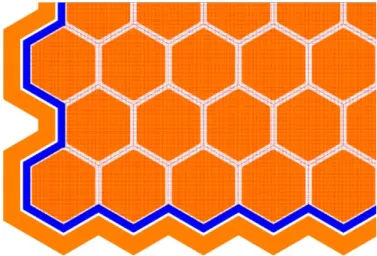
Prototyping phase is ongoing in the Max Planck Institute Semiconductor laboratory. Design phase is finished and Fig. 6 shows a layout example.
References
[1] M. Mandurah et al., J. Appl. Phys. 51 (11) (1980).
[2] Q.-Y. Tong, U. Go¨sele, Semiconductor Wafer Bonding, Wiley, NY, 1999.
[3] H. Gajewski, et al., TeSCA–Two Dimensional Semiconductor Analysis Package, Handbuch, WIAS, Berlin, 1997.
[4] ISE-TCAD Release 7.0, DIOS, vol. 2b, 2001.
[5] S. Cova, M. Ghioni, A. Lacaita, C. Samori, F. Zappa, Appl. Opt. 35 (1996) 1956.
ARTICLE IN PRESS
40 0 1x10⁻⁵ 2x10⁻⁵ 3x10⁻⁵ 4x10⁻⁵ 5x10⁻⁵ 6x10⁻⁵ 7x10⁻⁵
current [A]
Recovery times for 44V-->50V (90%) NB τrec
2.91011cm-2 -> 1.93μs 3.01012cm-2 -> 1.72μs 3.11012cm-2 -> 1.55μs
42 44 46 48 50
voltage [V]
quench condition
Fig. 5.Vertical resistors behave as parasitic JFETs leading to longer recovery times.
Illustrated are recovery times for three different bulk dopingðNBÞ. A quenching at 20mA is assumed [5].
Fig. 6.Layout example of an 125mm hexagonal cell: orange—high field implantation, red—cathode implantation, black—sub pixel boundaries and blue—aluminum lines.
integral charge [As]
1.5x10⁻¹³
1.0x10⁻¹³
5.0x10⁻¹⁴
0.0
1.0x10
-8
1.5x10
-8
time [s]
2.0x10
-8
2.5x10
-8
3.0x10
-8
3.5x10
-8
4.0x10
-8
Fig. 4.Simulated charge collection. The charge integral below 1 ns corresponds to the signal formation whereas the slower tail is associated with recovery of a cell.
J. Ninkovic´ et al. / Nuclear Instruments and Methods in Physics Research A 610 (2009) 142–144 144