Ming-Hao Liu (劉明豪),1,∗Peter Rickhaus,2P´eter Makk,2Endre T´ov´ari,3Romain Maurand,4 Fedor Tkatschenko,1Markus Weiss,2 Christian Sch¨onenberger,2and Klaus Richter1
1Institut f¨ur Theoretische Physik, Universit¨at Regensburg, D-93040 Regensburg, Germany
2Department of Physics, University of Basel, Klingelbergstrasse 82, CH-4056 Basel, Switzerland
3Department of Physics, Budapest University of Technology and Economics and Condensed Matter Research Group of the Hungarian Academy of Sciences, Budafoki ut 8, 1111 Budapest, Hungary
4University Grenoble Alpes, CEA-INAC-SPSMS, F-38000 Grenoble, France (Dated: April 10, 2017)
Artificial graphene consisting of honeycomb lattices other than the atomic layer of carbon have been shown to exhibit electronic properties similar to real graphene. Here, we show in the opposite logic that transport proper- ties of real graphene can be captured by simulations using “theoretical artificial graphene”. We derive a simple condition, along with its restrictions, to achieve band structure invariance for a scalable graphene lattice. Using the properly scaled artificial graphene, we perform quantum transport calculations within single-particle tight- binding models to simulate high-quality suspended graphenepnjunction devices. Good agreement between experiment and theory, for both zero-field- and magneto-transport, proves that the physics of real graphene can indeed be captured by studying the scaled graphene. Our findings indicate that transport simulations for graphene can be done with a much smaller number of atomic sites, paving the way to fully two-dimensional micron-scale graphene device simulations.
PACS numbers: 72.80.Vp, 72.10.-d, 73.23.Ad
Graphene is a promising material for its special electrical, optical, thermal, and mechanical properties. In particular, the conic electronic structure that mimics two-dimensional (2D) massless Dirac fermions attracts much attention on both the academic and industrial side. Soon after the “debut” of sin- gle layer graphene [1,2] and the subsequent confirmation of its relativistic nature [3,4], the exploration of Dirac fermions in condensed matter has been further extended to honeycomb lattices other than graphene, including optical lattices [5–7], semiconductor nanopatterning [8–11], molecular arrays on Cu(111) surface [12], or even macroscopic systems of di- electric resonators for microwave propagation [13,14], all of which have been shown to exhibit similar electronic proper- ties as real graphene and hence are referred to as artificial graphene [15].
Here, we show in the opposite logic that transport prop- erties of real graphene can be captured by simulations using
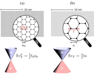
“theoretical artificial graphene“, by which we mean a hon- eycomb lattice with its lattice spacing a different from the carbon-carbon bond length a0 of real graphene; see Fig. 1.
From a theoretical point of view, this can be achieved only if the considered theoretical artificial lattice, which will be shortly referred to as artifical graphene or scaled graphene, has its energy band structure identical to that of real graphene. In this paper, we first derive a simple condition, along with its re- strictions, to achieve the band structure invariance of graphene with its bond length scaled froma0toa, even in the presence of magnetic field. We then present realistic conductance sim- ulations for a two-terminal suspended graphene device, using a properly scaled graphene. Good agreement between theory and experiment proves that the physics of real graphene can indeed be captured by studying artificial graphene. Notably, the feature of the measured conductance at zero magnetic field
can be well reproduced by our simulation even using a scaling factor of one hundred.
We begin our discussion with the standard tight-binding model for 2D graphite [16], i.e., bulk graphene, and fo- cus on the low-energy range (|E|.1 eV) which is usually addressed in transport measurements for graphene. In this regime, the effective Dirac HamiltonianHeff=vF~σ·passoci- ated with the celebrated linear band structureE(k) =±hv¯ F|k| describes the graphene system well. HerevF ≈108cm s−1 is the Fermi velocity in graphene, and ¯hk, the eigenvalue of the operator~σ·p[Pauli matrices~σ = (σx,σy)act on the pseudospin properties], is the quasimomentum withkdefined
(a)
10 nm
t0
a0 10x
N
P
¯
hv0F = 32t0a0
(b)
10 nm
t
a
10x
N
P
¯
hvF =32ta
FIG. 1. (Color online) Schematic of a sheet of (a) real graphene and (b) scaled graphene and their conical low-energy band structures.
In (a), the lattice spacinga0≈0.142 nm, the hopping energyt0≈ 2.8 eV, and the Fermi velocityv0F≈108cm s−1.
arXiv:1407.5620v1 [cond-mat.mes-hall] 21 Jul 2014
relative to theK or K0 point in the first Brillouin zone. In terms of the tight-binding parameters, one replaces ¯hvF with (3/2)t0a0, wheret0≈2.8 eV is the nearest neighbor hopping parameter and a0≈0.142 nm is the lattice site spacing, i.e., E0(k) = (3/2)t0a0k for real graphene [17]. Now, we con- sider the scaled graphene described by the same tight-binding model but with hopping parametert and lattice spacing a, and introduce a scaling factor sf such that a=sfa0. The real and scaled graphene sheets along with their low-energy band structures are schematically sketched in Fig.1. The low- energy dispersion for scaled graphene is naturally expected to beE(k) = (3/2)tak. Thus to keep the energy band structure unchanged while scaling up the bond length by a factor ofsf, the condition
a=sfa0, t= t0
sf. (1)
becomes evident.
Clearly, Eq. (1) applies only when the linear approximation is valid. In terms of the long wavelength limit, this means that the Fermi wavelength should be much longer than the lattice spacing: λFa, from which using Eq. (1) one can deduce the validity criterion
sf 3t0π
|Emax|, (2) whereEmaxis the maximal energy of interest for investigating a particular real graphene system. Considering graphene on typical Si/300nm SiO2substrate, the usually accessed carrier density range is less than 1013cm−2[1]. This implies that the energy range of interest lies within|Emax|.0.4 eV, leading tosf 66 from Eq. (2) (usingt0=2.8 eV). For suspended graphene, typical carrier densities can hardly reach 1012cm−2 [18], so that|Emax|.0.1 eV allows for a larger range of the scaling factor,sf 264.
In the presence of an external magnetic field, the Peierls substitution [19] is the standard method to take into account the effect of a uniform out-of-plane magnetic fieldBzwithin the tight-binding formulation. In addition to the long wave- length limit (2), the validity of the Peierls substitution, how- ever, imposes a further restriction for the scaling [20]:lBa, where lB=p
h/eB¯ z is the magnetic length. In terms of a=sfa0given in Eq. (1), this restriction reads
sf lB a0 ≈ 180
√Bz, (3) whereBz is in units of T. Equations (1)–(3) complete the description of band structure invariance for scaled graphene.
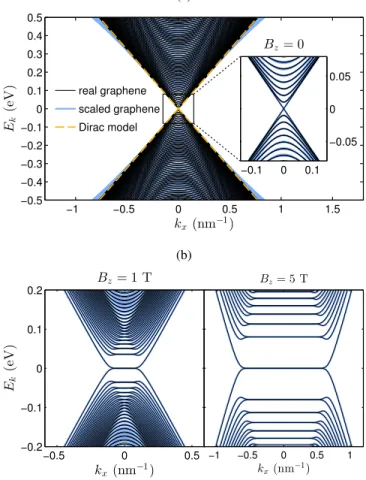
The above discussion is based on bulk graphene, but the listed conditions apply equally well to finite-width graphene ribbons. To show a concrete example of band structure invari- ance under scaling, we consider a 200-nm-wide armchair rib- bon and compare the band structures of the genuine case with sf =1 and the scaled case withsf =4, as shown in Fig.2(a).
Within the relatively large energy range of|E| ≤0.5 eV, the
(a)
kx (nm−1) Ek(eV)
Dirac model real graphene scaled graphene
−1 −0.5 0 0.5 1 1.5
−0.5
−0.4
−0.3
−0.2
−0.1 0 0.1 0.2 0.3 0.4 0.5
Bz= 0
−0.1 0 0.1
−0.05 0 0.05
(b)
kx(nm−1) Ek(eV)
Bz= 1 T
−0.5 0 0.5
−0.2
−0.1 0 0.1 0.2
kx(nm−1) Bz= 5 T
−1 −0.5 0 0.5 1
FIG. 2. (Color online) Band structure consistency check using an armchair graphene ribbon with width 200 nm, (a) in the absence of magnetic field, and (b) in the presence of a uniform magnetic field Bz=1 T (left) andBz=5 T (right). Inset in (a) shows the zoom-in plot for the boxed region of the main panel. The comparison is done for both (a) and (b) between the real graphene withsf=1 and scaled graphene withsf=4, which correspond to chain numbersNa=800 andNa=200, respectively.
genuine graphene band structure is well bound by the linear Dirac model that corresponds to the ideal bulk graphene. On the other hand, the scaled graphene band structure starts to ex- hibit a nonlinear cone shape at about|E|&0.2 eV, where the long wavelength limit (2) no longer holds. In the low energy range [inset of Fig.2(a)], one observes a nearly perfect con- sistency between the genuine and scaled graphene band struc- tures. The model remains consistent when a magnetic field is applied, as seen in Fig.2(b), where we considerBz=1 T and 5 T, both of which still lie within the restriction (3) for the presentsf =4 example. The band structure invariance based on Eqs. (1)–(3) can be easily shown to hold also for zigzag graphene ribbons.
Having demonstrated that under proper conditions (1)–(3) the scaled graphene band structure can be identical to that of real graphene, we next perform full quantum transport simu- lations using scaled graphene, taking into account the three- dimensional geometry of a real experimental graphene de-
vice. To this end, we have fabricated ultra-clean suspended graphenepnjunctions. First, bottom gates were prepatterned on a Si wafer with 300 nm SiO2oxide. Afterwards, the wafer was spin-coated with lift-off resist (LOR), and the graphene was transferred on top following the method described in Ref.
21. Palladium contacts to graphene were made by e-beam lithography and thermal evaporation, and the device was sus- pended, by exposing and developing the LOR resist. Finally, the graphene was cleaned by current annealing at 4 K. The fabrication method is described in Refs.22and23in detail.
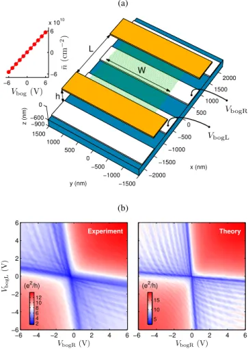
Following the device design of our experiment [sketched in Fig.3(a)with actual dimensions adopted in the simulation], we first build the three-dimensional (3D) electrostatic model to obtain the self-partial capacitances [24] of the individual metal contacts and bottom gates, which are computed by the finite-element simulator FEniCS [25] combined with the mesh generator GMSH [26]. The extracted self-partial capacitances from the electrostatic simulation provide us the realistic car- rier density profile [27]n(x,y)at any combination of the left and right bottom gate voltages,VbogLandVbogR, respectively.
In the inset of Fig.3(a), we plot the mean carrier density ¯nav- eraged over the whole suspended graphene region as a func- tion ofVbog=VbogL=VbogR. The slope reveals a charging effi- ciency of the connected bottom gates of about 1010cm−2V−1, which will be later compared with the experimental value ex- tracted from the unipolar quantum Hall data.
In the absence of magnetic field, the Fermi energy as a function of carrier density within the low-energy range can be well described by the Dirac model,E(n) =sgn(n)¯hvFp
π|n|. This suggests: for a given carrier density at (x,y), ap- plying a local energy band offset defined by V(x,y) =
−sgn[n(x,y)]¯hvFp
π|n(x,y)|guarantees that the locally filled highest level fulfills the amount of the simulated carrier den- sityn(x,y)and is globally fixed at E =0 for all(x,y). We therefore consider the model Hamiltonian,
Hmodel=
∑
i
V(xi,yi)c†ici−t(sf)
∑
hi,ji
c†icj, (4) and apply the Landauer-B¨uttiker formalism [28] to calculate the transmission functionT at energyE=0 and zero temper- ature. In Eq. (4), the indicesiand jrun over the lattice sites within the scattering region defined by an artificial graphene scaled bysf, and the second term contains the nearest neigh- bor hopping elements with strengtht(sf)given in Eq. (1).
For zero-field transport, we compute the conductance map G(VbogR,VbogL)from the transmission functionT usingG= (e2/h)[T−1+Rc/(h/e2)]−1, where the contact resistance is deduced from the quantum Hall measurement to be Rc ≈ 1080Ω≈4.2×10⁻²(h/e2). The measured and simulated conductance maps in the absence of magnetic field are com- pared in Fig.3(b). Both exhibit pronounced Fabry-P´erot inter- ference patterns in the bipolar blocks similar to previously re- ported ballistic graphenepnjunctions [29,30]. Strikingly, the theory data reported in Fig.3(b)is based on a scaled graphene withsf =100, and the result agrees qualitatively well with the experiment. The present device allows for such a huge
(a)
−2000
−1500
−1000
−500 0
500 1000
1500 2000
−1500
−1000
−500 0 500 1000 1500
−900
−600 0
x (nm)
W L
y (nm)
h
z (nm)
−6 0 6
−6 0 6 x 10¹⁰
Vbog(V)
¯n(cm−2)
VbogL VbogR
(b)
VbogR(V) VbogL(V)
Experiment
−6 −4 −2 0 2 4 6
−6
−4
−2 0 2 4 6
(e2/h)
2 4 6 8 10 12
VbogR(V) Theory
−6 −4 −2 0 2 4 6
(e2/h)
5 10 15
FIG. 3. (Color online) (a) Device sketch of the suspended graphene for electrostatic modeling and transport simulation, following the ex- periment design with suspension heighth=600 nm, contact spacing L=1680 nm, and average flake widthW =2125 nm. Inset: Mean carrier density as a function of the voltage on the two bottom gates when they are connected to each other,VbogL=VbogR=Vbog, based on a 3D electrostatic simulation. (b) Experimental and theoretical data of the two-terminal conductance. The former was measured at low temperatureT=1.4 K, while the latter was calculated by using an idealsf=100 scaled clean graphene at zero temperature.
scaling factor due to the very low energy. From the esti- mated maximal carrier density [inset of Fig.3(a)], we find
|Emax| ≈28 meV, such that Eq. (2) roughly givessf 103, suggesting that sf =100 is acceptable. Simulations with smallersf have been performed and do not significantly differ from the reported map.
Similar to the zero-field case, the first step for an accurate transport simulation at finiteBz is to extract the proper en- ergy band offset from the given carrier density through the carrier-energy relation, for which an exact analytical formula does not exist. Numerically, the carrier density as a function of energy and magnetic field,n(E,Bz), can be computed also using the Green’s function method [27]. Oncen(E,Bz)is ob- tained, one can deduceE(n,Bz)by interpolation, and the de- sired energy band offset is again given by the negative of it.
Thus the magnetic field in the transport simulation requires, in addition to the Peierls substitution of the hopping param- eter, the modification on the on-site energy term of Eq. (4), V(xi,yi)→V(xi,yi;Bz) =−E(n(xi,yi),Bz), wheren(xi,yi)is obtained from the same electrostatic simulation and is as- sumed to be unaffected by the magnetic field, i.e., we assume the electrostatic charging ability of the bottom gates is not in- fluenced by the magnetic field.
Figure4(a)shows the measured unipolar conductance map G(Bz,Vbog) with the two bottom gates connected together.
The pronounced fan diagram allows for a precise evalua- tion of the gate efficiency and chemical doping concentra- tion [27], which are found to be 1.24×1010cm−2V−1 and
−3.72×109cm−2, respectively. By subtracting the contact re- sistanceRc≈1080Ω, the quantized conductance at low field up to 0.2 T is compared with the computed transmission func- tion using sf =50 scaled graphene in Fig.4(b), where the color range is adjusted to highlight the conductance plateaus up toν=±14.
Despite the rather consistent Landau fan diagrams in both experiment and theory maps of Fig.4(b), a closer look shows the slightly different gate efficiencies (slope of the fan lines) as already noted above. In addition, the minimalBz required to quantize the conductance in the experiment is larger than that in the simulation possibly because of thermal fluctuations not considered in the calculations. Note that here we have considered Anderson-type disorder by adding to the model Hamiltonian (4) the potential term ∑iUic†ici, whereUi is a random numberUi∈[−Udis/2,Udis/2]with disorder strength Udis=3 meV used in the theory map of Fig.4(b). The quan- tized conductance in the simulation is found to be robust against the disorder potential, whose quantitative effect is yet to be established for the scaled graphene and is beyond the
(a)
Bz(T)
Vbog(V) ν= +2
ν=−2 +6 +10
−6
−10
0 0.5 1
−15
−10
−5 0 5 10 15
(e2/h)
0 5 10 15
(b)
Bz(T) Vbog(V)
Experiment
0 0.1 0.2
−6
−4
−2 0 2 4 6
2 6 10 14
Bz(T) Theory
0 0.1 0.2
−6
−4
−2 0 2 4 6
2 6 10 14
FIG. 4. (Color online) (a) Experimental data of the conductance mea- sured with the two bottom gates connected to each other (VbogL= VbogR=Vbog) and magnetic fieldBz sweep up to 1 T. The low- est 6 quantized conductance plateaus labeled by filling factorν=
±2,±6,±10 are separated by the fitting fan lines [27]. (b) By sub- tracting the deduced contact resistanceRc≈1080Ω, the experimen- tal data at low field is compared with the theory data of the computed transmission function.
VbogR(V) VbogL(V)
Experiment
−6 −4 −2 0 2 4 6
−6
−4
−2 0 2 4 6
(e2/h)
2 4 6 8
VbogR(V) Theory
−6 −4 −2 0 2 4 6
(e2/h)
2 4 6 8
FIG. 5. (Color online) ConductanceG(VbogR,VbogL)measured (left) and simulated (right) atBz=0.2 T. The simulation is based onsf = 50 artificial graphene in the presence of Anderson-type disorder with fluctuation strengthUdis=6 meV.
scope of the present discussion.
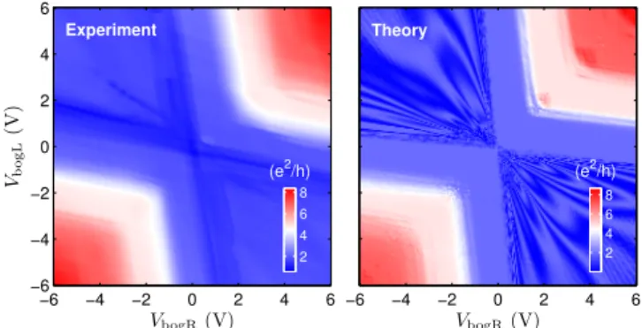
Finally, we compare the conductance mapsG(VbogR,VbogL) measured and simulated atBz=0.2 T in Fig.5, usingsf=50 scaled graphene in the presence of disorder potential with Udis=6 meV. We observe very good agreement in the con- ductance range as well as in the conductance features in the unipolar blocks. In the bipolar blocks, however, the simu- lation reveals a fine structure that is found to be sensitive to disorder potential and the edge disorder, but is not observed in the present experimental data. Nevertheless, the conduc- tance in the bipolar blocks varies between 0 and 2e2/hin both experiment and theory, and neither of them exhibits the frac- tional plateaus [31]. Thus the bipolar blocks of Fig.5reveal a conductance behavior due to the ballistic smooth graphenepn junctions very different from the diffusive sharp ones [32–34].
In conclusion, we have shown that the physics of real graphene can be well captured by studying properly scaled, artificial graphene. This important fact indicates that for low-energy transport simulations in graphene based on tight- binding models, the required number of lattice sites need not be as massive as in actual graphene sheets. The introduced parametersf scales down the amount of the Hamiltonian ma- trix elements of the simulated graphene flake by a factor of s−f4, and hence strongly reduces the memory demand [27];
the scaling applies also to bilayer graphene [27]. Our find- ings advance the power of quantum transport simulations for graphene in a simpler and more natural way as compared to the finite difference method for massless Dirac fermions [35], paving the way to fully 2D micron-scale graphene device sim- ulations.
We thank J. Bundesmann, S. Essert, and V. Krueckl and J. Michl for valuable suggestions. Financial support by the Deutsche Forschungsgemeinschaft within programs GRK 1570 and SFB 689, by the Hans B¨ockler Foundation, by the Swiss NSF, the EU FP7 project SE2ND, the ERC Ad- vanced Investigator Grant QUEST, the ERC 258789, the Swiss NCCR Nano QSIT, and Graphene Flagship is gratefully acknowledged.
∗ minghao.liu.taiwan@gmail.com
[1] K. S. Novoselov, A. K. Geim, S. V. Morozov, D. Jiang, Y. Zhang, S. V. Dubonos, I. V. Grigorieva, and A. A. Firsov, Science306, 666 (2004).
[2] C. Berger, Z. Song, T. Li, X. Li, A. Y. Ogbazghi, R. Feng, Z. Dai, A. N. Marchenkov, E. H. Conrad, P. N. First, and W. A. de Heer,The Journal of Physical Chemistry B108, 19912 (2004).
[3] Y. Zhang, Y.-W. Tan, H. L. Stormer, and P. Kim,Nature438, 201 (2005).
[4] K. S. Novoselov, A. K. Geim, S. V. Morozov, D. Jiang, M. I.
Katsnelson, I. V. Grigorieva, S. V. Dubonos, and A. A. Firsov, Nature438, 197 (2005).
[5] S.-L. Zhu, B. Wang, and L.-M. Duan,Phys. Rev. Lett. 98, 260402 (2007).
[6] B. Wunsch, F. Guinea, and F. Sols,New Journal of Physics10, 103027 (2008).
[7] T. Uehlinger, G. Jotzu, M. Messer, D. Greif, W. Hofstetter, U. Bissbort, and T. Esslinger,Phys. Rev. Lett.111, 185307 (2013).
[8] C.-H. Park and S. G. Louie, Nano Letters 9, 1793 (2009), http://pubs.acs.org/doi/pdf/10.1021/nl803706c.
[9] M. Gibertini, A. Singha, V. Pellegrini, M. Polini, G. Vignale, A. Pinczuk, L. N. Pfeiffer, and K. W. West,Phys. Rev. B79, 241406 (2009).
[10] E. R¨as¨anen, C. A. Rozzi, S. Pittalis, and G. Vignale,Phys. Rev.
Lett.108, 246803 (2012).
[11] E. Kalesaki, C. Delerue, C. Morais Smith, W. Beugeling, G. Al- lan, and D. Vanmaekelbergh,Phys. Rev. X4, 011010 (2014).
[12] K. K. Gomes, W. Mar, W. Ko, F. Guinea, and H. C. Manoharan, Nature483, 306 (2012).
[13] U. Kuhl, S. Barkhofen, T. Tudorovskiy, H.-J. St¨ockmann, T. Hossain, L. de Forges de Parny, and F. Mortessagne,Phys.
Rev. B82, 094308 (2010).
[14] M. Bellec, U. Kuhl, G. Montambaux, and F. Mortessagne, Phys. Rev. B88, 115437 (2013).
[15] M. Polini, F. Guinea, M. Lewenstein, H. C. Manoharan, and V. Pellegrini,Nature Nanotechnology8, 625 (2013).
[16] P. R. Wallace,Phys. Rev.71, 622 (1947).
[17] Note that the next nearest neighbor hoppingt0does not play a role for describing the low-energy physics of graphene, and will not be considered in this work.
[18] K. Bolotin, K. Sikes, Z. Jiang, M. Klima, G. Fudenberg, J. Hone, P. Kim, and H. Stormer,Solid State Communications 146, 351 (2008).
[19] R. Peierls,Zeitschrift f¨ur Physik A Hadrons and Nuclei80, 763 (1933), 10.1007/BF01342591.
[20] M. O. Goerbig,Rev. Mod. Phys.83, 1193 (2011).
[21] C. R. Dean, A. F. Young, I. Meric, C. Lee, L. Wang, S. Sorgen- frei, K. Watanabe, T. Taniguchi, P. Kim, K. L. Shepard, and J. Hone,Nature Nanotechnology5, 722 (2010).
[22] N. Tombros, A. Veligura, J. Junesch, J. Jasper van den Berg, P. J. Zomer, M. Wojtaszek, I. J. Vera Marun, H. T. Jonkman, and B. J. van Wees,Journal of Applied Physics109, 093702 (2011).
[23] R. Maurand, P. Rickhaus, P. Makk, S. Hess, E. Tovari, C. Hand- schin, M. Weiss, and C. Sch¨onenberger, “Fabrication of ballis- tic suspended graphene with local-gating,” (2014), submitted.
[24] D. K. Cheng,Field and Wave Electromagnetics, 2nd ed. (Pren- tice Hall, 1989).
[25] A. Logg, K.-A. Mardal, G. N. Wells,et al.,Automated Solu-
tion of Differential Equations by the Finite Element Method (Springer, 2012).
[26] C. Geuzaine and J.-F. Remacle, International Journal for Nu- merical Methods in Engineering79, 1309 (2009).
[27] See supplemental material for numerical examples of the carrier density profilen(x,y)simulated for the device, the carrier den- sity as a function of energy and magnetic fieldn(E,Bz)using scaled graphene ribbons, evaluation of the gate efficiency from the Landau fan diagram shown in Fig.4(a), and comments on the speed-up and bilayer graphene.
[28] S. Datta,Electronic Transport in Mesoscopic Systems(Cam- bridge University Press, Cambridge, 1995).
[29] A. L. Grushina, D.-K. Ki, and A. F. Morpurgo,Appl. Phys.
Lett.102, 223102 (2013).
[30] P. Rickhaus, R. Maurand, M.-H. Liu, M. Weiss, K. Richter, and C. Sch¨onenberger,Nature Communications4, 2342 (2013).
[31] D. A. Abanin and L. S. Levitov,Science317, 641 (2007).
[32] J. R. Williams, L. DiCarlo, and C. M. Marcus,Science317, 638 (2007).
[33] B. ¨Ozyilmaz, P. Jarillo-Herrero, D. Efetov, D. A. Abanin, L. S.
Levitov, and P. Kim,Phys. Rev. Lett.99, 166804 (2007).
[34] W. Long, Q.-f. Sun, and J. Wang,Phys. Rev. Lett.101, 166806 (2008).
[35] J. Tworzydło, C. W. Groth, and C. W. J. Beenakker,Phys. Rev.
B78, 235438 (2008).
[36] M.-H. Liu,Phys. Rev. B87, 125427 (2013).
[37] G. Li and E. Y. Andrei,Nat. Phys.3, 623 (2007).
[38] E. McCann and M. Koshino,Reports on Progress in Physics76, 056503 (2013).
Supplemental Material
Carrier density profile of the simulated device
As mentioned in the main text, the finite-element simu- lator FEniCS [25] together with the mesh generator GMSH [26] are adopted to compute the self-partial capacitances [36] of the individual metal contacts and bottom gates, CcL,CcR,CbogL, and CbogR, which are functions of two- dimensional coordinates(x,y). The classical contribution to the total carrier densityn(x,y)is given by the linear combina- tion∑i=cL,cR,bogL,bogR(Ci/e)Vi, whereVbogLandVbogRare the left and right bottom gate voltages, respectively, andVcLand VcRare responsible for contact doping mainly arising from the charge transfer between the metal contacts and the graphene sheet. Since the experimental conditions are very similar to our previous work [30], we adopt the same empirical value of 0.04 V for bothVcLandVcR. Total carrier density follows Ref.
36. Two examples showing n(x,y)profiles are given in Fig.
S1, where zero intrinsic doping is assumed.
Carrier-energy relation in the presence of magnetic field To compute the carrier density as a function of energyEand magnetic fieldBzusing the Green’s function method, we con- sider an ideal graphene ribbon extending infinitely along the
±xaxis. The retarded Green’s function tells the total density
(a)
VbogL
3V
VbogR
5V
L contact R contact
x(nm)
y(nm)
−890 −290 290 890
−1000
−500 0 500 1000
n(x,y)(cm−2)
3 4 5 6 7 8 x 10¹⁰
(b)
VbogL
2V
VbogR
−4V
L contact R contact
x(nm)
−890 −290 290 890 n(x,y)(cm−2)
−4
−2 0 2 4 x 10¹⁰
FIG. S1. Examples of carrier density profilesn(x,y)with (a) unipolar and (b) bipolar gate voltage configurations. Bottom gate voltages are indicated in respective plots. The geometry follows the design values of the experiment, and the shape of the graphene flake is estimated from an optical image of the real device. The width of the bottom gates is 600 nm, and the white dashed lines indicate the edges of the bottom gates underneath the contacts.
of states of the supercell,D(E,Bz) =−(1/π)Im TrGr(E,Bz), where we have explicitly denoted the dependence of the mag- netic fieldBz, which enters from the tight-binding Hamilto- nian of the supercell. The carrier density in the zero temper- ature limit is given by integrating over the energy,n(E,Bz) = (2/A)R0ED(E0,Bz)dE0, where the factor 2 accounts for the spin degeneracy andA=N(3√
3a2/4)is the area of the su- percell withNthe number of lattice sites within the supercell anda=sfa0the lattice spacing.
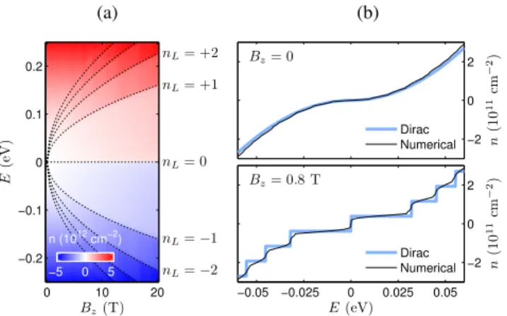
An example forn(E,Bz)using a scaled armchair graphene ribbon withsf =4 andNa=101 (about 100 nm wide) is given in Fig. S2(a). With the increasingBz, the emergence of the relativistic Landau level spectrum [37] is clearly seen, which
(a)
Bz(T)
E(eV)
nL=−2 nL=−1 nL= 0 nL= +1 nL= +2
0 10 20
−0.2
−0.1 0 0.1 0.2
n (1012 cm−2)
−5 0 5
(b)
−2 0 2
n(1011cm−2) Bz= 0
Dirac Numerical
−0.05 −0.025 0 0.025 0.05
−2 0 2
E(eV)
n(1011cm−2) Bz= 0.8 T
Dirac Numerical
FIG. S2. (a) Carrier density as a function of energyE and mag- netic fieldBz, using ansf =4,Na=101 artificial armchair graphene ribbon (about 100 nm wide). The quantized carrier density is well described by the Landau level spectrum (dashed lines) given by Eq. (S1). (b) Carrier-energy relation at Bz=0 (upper panel) and Bz=0.8 T (lower panel), using ansf =16,Na=50 ribbon (about 200 nm wide). The numerical results are compared with the Dirac model, Eq. (S2) in the upper panel and Eq. (S3) in the lower panel.
is well described by EnL=sgn(nL)E1
p|nL| E1=
q 2eBzhv¯ 2F
, nL=0,±1,±2,···. (S1) Thus properly scaled graphene also correctly captures the half integer quantum Hall physics of real graphene.
In Fig. S2(b) we use another ribbon with sf =16 and Na=50 (about 200 nm wide) to compare the carrier-energy relation with and without magnetic field. For theBz=0 case [upper panel in Fig.S2(b)], despite the ribbon nature of the considered artificial graphene, then(E) relation is basically consistent with the Dirac model,
nDirac(E) =sgn(E)1 π
E
¯ hvF
2
. (S2)
For theBz=0.8 T case [lower panel in Fig. S2(b)], the nu- merical result exhibits quantized plateaus due to the Landau levels. The plateaus are, however, not perfectly flat due to the level broadening of the density of states, which stems from the finite width of the considered ribbon, instead of temperature.
In the case of ideal infinite graphene, the density of states can be written as DDirac(E,Bz) = (4eBz/h)∑nLδ(E−EnL), where the prefactor accounts for the states each Landau level can accommodate andEnL is given in Eq. (S1). Integrating DDirac(E,Bz)with respect to energy, one obtains a perfectly quantized carrier-energy relation
nDirac(E,Bz) =4eBz h
sgn(E)
E2 E12
+1 2
, (S3)
wherebxc stands for the largest integer not greater than x (known as the floor function in computer science) andE1is given in Eq. (S1). Compared to the numericaln(E,Bz)[lower panel in Fig.S2(b)], the idealnDirac(E,Bz)given by Eq. (S3) is not suitable for describing the carrier-energy relation in finite- width graphene systems. Nevertheless, the formula confirms the correct trend of the numerical carrier-energy relation in the presence of magnetic field.
From the numericaln(E)curve at a givenBz, such as that given in Fig.S2(b), the position of the highest filled energy level for a given carrier density, E(n), is obtained, and the negative of it is the desired energy band offset for transport calculation as mentioned in the main text.
Gate efficiency from the Landau fan diagram
The pronounced quantized conductance plateaus reported in Fig.4(a)of the main text allows for a precise evaluation of the gate efficiency. Let the average gate capacitance of the connected bottom gates be ¯Cgand assume a uniform chemical doping of concentrationn0. Relating the mean carrier density given by ¯n=n0+C¯gVbogand filling factorν=n/(eB¯ z/h)one finds
Vbog= eν
C¯ghBz−n0
C¯g≡c1νBz+c2.
Thus on the field-gate map reported in Fig.4(a)of the main text, the slope of each fan line that separates two adjacent con- ductance plateausν−2 andν+2 givesc1ν=eν/C¯ghwhile the intersect atBz=0 givesc2=−n0/C¯g. By fitting the ex- perimental data atν=0,±4,···, we findc1=1.95 V T−1and c2=0.3 V, which yield a gate efficiency
C¯g= e
c1h=1.24×1010cm−2V−1 and a weak chemical doping
n0=−c2C¯g=−3.72×109cm−2,
respectively. The deduced ¯Cg is found to be slightly larger than the simulation [inset of Fig.3(a)of the main text].
Comments on speed-up and bilayer graphene
The strongly reduced memory demand due to the scaling naturally lowers the computation time. Even for computable systems, the speed-up can be seen in, e.g., the computation time∆tfor the lead self-energy that typically grows with the cube of the number of lattice sites within the lead supercell, i.e., ∆t →∆t/s3f after scaling. Taking the illustrated 2.2- micron-wide graphene for example,∆tis found to be∼2.4 s
on a single Intel Core i7 CPU for the artificial graphene scaled bysf =100. Forsf =1, the time required to compute just a single shot of the self-energy, if the memory allows, would be
∼2.4×(100)3s, which is almost a month.
The scaling can easily be shown to be applicable to bilayer graphene, whose low-energy spectrum is given by [38]
E(k) =± v u u tγ12
2 +U2
4 +h¯2v2Fk2± s
γ14
4 +h¯2v2Fk2 γ12+U2 , (S4) withγ1≈0.39 eV the interlayer nearest neighbor hopping and Uthe asymmetry parameter responsible for the gap. The ap- pearance of the producttain the dispersion (S4) after substi- tuting ¯hvF=3ta/2 clearly suggests that the scaling condition [Eq. (1) of the main text] also applies for bilayer graphene withγ1andU left unaltered. Similar to the long wavelength limit [Eq. (2) of the main text] but due to the massive Dirac nature, the limit ofsf becomes stricter. In the case of gap- less bilayer graphene, we havesf 6πt0/[(2|Emax|+γ1)2− γ12]1/2, which suggestssf 50 for the single-band transport (|Emax| ≤γ1). In the presence of magnetic field, the restriction of Eq. (3) in the main text still applies.