Supplemental Material:
Evidence for phonon skew scattering in the spin Hall effect of platinum
G. V. Karnad,1 C. Gorini,2,∗ K. Lee,1 T. Schulz,1 R. Lo Conte,1, 3 A.
W. J. Wells,4 D.-S. Han,1, 5 K. Shahbazi,4 J.-S. Kim,5,† T. A. Moore,4 H. J. M. Swagten,5 U. Eckern,6 R. Raimondi,7 and M. Kl¨aui1, 3,‡
1Institut f¨ur Physik, Johannes Gutenberg-Universit¨at, Staudinger Weg 7, 55128 Mainz, Germany
2Institut f¨ur Theoretische Physik, Universit¨at Regensburg, 93040 Regensburg, Germany
3Graduate School of Excellence “Materials Science in Mainz”(MAINZ), Staudinger Weg 9, 55128 Mainz, Germany
4School of Physics and Astronomy,
University of Leeds, Leeds LS2 9JT, United Kingdom
5Department of Applied Physics, Eindhoven University of Technology, 5600 MB Eindhoven, The Netherlands
6Institut f¨ur Physik, Universit¨at Augsburg, 86135 Augsburg, Germany
7Dipartimento di Matematica e Fisica, Roma Tre University, Via della Vasca Navale 84, 00146 Rome, Italy
(Dated: March 22, 2018)
MATERIAL DEPOSITION
The material stack: Ta(4.0)|Pt(4.0)|Co(1.3)|AlOx(2.0) (all thicknesses in nm) is deposited onto a Si|SiO2 substrate by DC magnetron sputtering with a base pressure of ≈ 7×10⁻⁸ mbar. The capping layer of AlOx is obtained by plasma oxidation of the Al deposited on Co. The plasma oxidation is carried out in an in-situ isolated chamber for 10 min with 0.1 mbar oxygen background pressure at 15 W.
Deposition conditions
Material Working pressure (Pa) Sputter power (W)
Tantalum 1.4 20
Platinum 0.29 60
Cobalt 1 20
Aluminium 1 20
The stack is characterized using MOKE microscopy and is found to exhibit a perpendic- ular magnetic anisotropy.
DEVICE FABRICATION
The thin film deposited on the Si|SiO2 substrate is used to pattern the Hall bar structures.
To perform the transport measurements we use e-beam lithography and ion milling to pattern Hall-bar devices (1-2 µm in width and 50 µm in length). In the first lithography step and milling process we define the Hall bars with small contact pads. In the second lithography step we define the larger contact pads (which overlap the small contact pads) and etch until (monitored using a mass spectrometer) we are in contact with the Pt under layer. The larger contacts for the Hall bars consist of Cr(10 nm)|Au(120 nm) which are sputter deposited after the second lithography step to make the final contacts.
RESISTANCE MEASUREMENT
The sheet resistivity of the sample is measured in two geometries: Hall-bar and thin-film sample. The residual resistivity of the samples is measured at 3 K. At this temperature, it can be assumed that the contribution to the resistivity is purely a result of the impurities
- 1 0 0 - 5 0 0 5 0 1 0 0 - 1 . 0 5
1 . 1 0 1 . 1 5
H ( m T )
V
1ω(m V )
- 1
01
V
2ω( µ V )
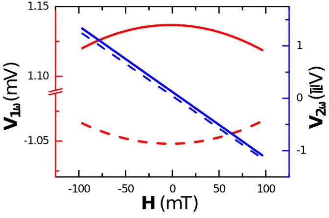
Fig. S1. Longitudinal scheme: First (red−−linear fit) and second harmonic (blue−−2nd order polynomial fit) voltages fitting for up (solid line) and down (dashed line) magnetization. Measured at 300 K
present in the system and which is not expected to change with temperature. Due to the fact that Pt has the smallest resistivity in the multilayer system, it can be expected that the majority of the current passes through this layer. The residual resistivity of the Hall-bar geometry is thus found to be 3.8µΩcm. A van der Paauw [1] measurement is also performed on a thin film sample (2.5 mm x 2.5 mm), and we find the residual sheet resistivity to be 5.3 µΩcm.
SECOND-HARMONICS MEASUREMENT
The measurements are performed in a 3D vector cryostat. The 3D vector magnet set-up allows to address the magnetization in the complete 3-dimensional space. This allows us to unambiguously extract the appropriate current induced effective fields by studying the
- 0 . 1 0 - 0 . 0 5 0 . 0 0 0 . 0 5 0 . 1 0 - 1 . 1
- 1 . 0 1 . 1
H ( m T )
V
1ω(m V )
- 0 . 5 0 . 0 0 . 5
V
2ω( µ V )
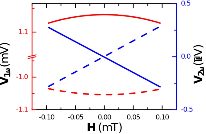
Fig. S2. Transversal scheme: First (red−−linear fit) and second harmonic (blue−−2nd order polynomial fit) voltages fitting for up (solid line) and down (dashed line) magnetization. Measured at 300 K.
angular dependence of the fields and the symmetry of the exerted torques. The injection of an ac current signal results in the perturbation of the magnetization in the ferromagnet away from its equilibrium position. This results in the change of the Hall voltage. To extract the SOT effective fields, the measurements are performed under the application of external magnetic fields in two schemes: 1. longitudinal: along the x-axis (damping-like), and 2.
transversal: along the y-axis (field-like). In the longitudinal scheme,V1ωexhibits a parabolic shape and its sign depends on the direction of the magnetization (Fig. S1). Results for the transversal scheme are identical. In case of the V2ω, in the transversal scheme it exhibits linear behavior, which has opposite slopes depending on the magnetization (Fig. S2). In the case of the longitudinal scheme they have the same slopes (Fig. S1) resulting from the symmetry of the torques. The effective fields can be extracted by measuring the first (V1ω) and second harmonic (V2ω) signal of the Hall voltage and is expressed by [2–4] Eqn.1, where
the term BL,T is the relation between V2ω and V1ω for both longitudinal and transversal directions:
BL,T = ∂V2ω
∂H
∂2V2ω
∂H2 (1)
The variation of the Hall voltage has various contributions such as Nernst effect, Joule heating, anomalous Hall effect, and planar Hall effect. This is taken [3, 4] into account before extracting the spin-orbit torque effective fields. The final expression relating the hall voltage with the SOT effective fields (HL and HT) is given by [3, 4] Eqn. 2 and Eqn. 3, where ξ = ∆R∆RP HE
AHE is the ratio of the planar Hall effect resistance and the anomalous Hall effect resistance:
∆HL=−2BL±2ξBT
1−4ξ2 (2)
∆HT =−2BT ±2ξBL
1−4ξ2 (3)
ADDITIONAL CONTROL MEASUREMENTS
a) Pt based sample
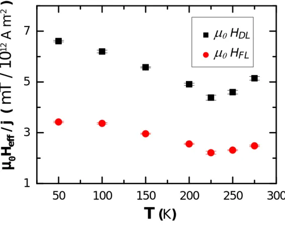
An additional control sample stack for “clean” Pt(Pt(4 nm)|Co(0.8 nm)|AlOx(2 nm)) was grown to confirm the origin of the non-monotonic behavior observed in Fig. 3 (main manuscript). In comparison to the sample discussed in the manuscript, this was grown in a different sputter chamber (at University of Leeds) and the growth process was optimized accordingly. A thin film of Pt was used for the measurement of the resistivity, and we find a residual resistivity of 6.3 µΩcm (Fig. S7). We observe from Fig. S3 and Fig. S4 that the spin orbit torque measurements are consistent with the results obtained from the sample used for the main text and thus this system yields a reproducible and robust temperature dependence of the torques that is not very sensitive to the specific details of the growth (working pressure, sputter power etc.: which tends to vary slightly from deposition chamber to deposition chamber). This confirms that the observation is not unique to the growth process in one single chamber and is reproducible in a “clean” Pt based sample. Fig. S5 and Fig. S6 confirm the non-monotonous behavior of the spin Hall resistivity as a function
5 0 1 0 0 1 5 0 2 0 0 2 5 0 3 0 0
1357 H D L
H F L
m 0H eff / j ( mT / 1012 A m-2 ) T ( K )
Fig. S3. The efficiency of the damping-like (µ0HDL) and field-like (µ0HF L) spin orbit torque effective field is given as a function of temperature. The behavior is found to be in agreement with that found for the other Pt based sample presented in the main manuscript (Fig. 3).
of total resistivity. This prevents the application of a simple linear equation (as done in Ref.
[24] of the main manuscript) to describe the evolution of the SHA with temperature.
b) Ta based sample
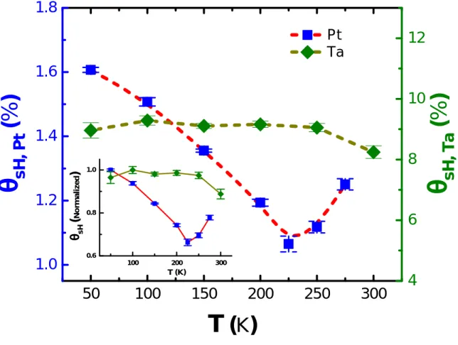
The temperature dependence of the SHA, extracted from the spin-orbit torques, was measured also in a sample of tantalum (|Ta(5 nm)|CoFeB(1 nm)|MgOx(2 nm)). The Ta sample is used to measure the evolution of the SHA as a function of temperature in a sample with higher residual resistivity (136.52 µΩcm). We observe that despite the linear increase of the resistivity (Fig. S7) in the 50−−300 K range, the SHA remains rather constant (Fig. S4). This is in line with the theoretical expectation that one is expected to
5 0 1 0 0 1 5 0 2 0 0 2 5 0 3 0 0 1 . 0
1 . 2 1 . 4 1 . 6 1 . 8
P t T a
T ( K )
q
sH, Pt (%) 4681 0 1 2
1 0 0 2 0 0 3 0 0
0 . 6 0 . 8 1 . 0
qsH(Normalized)
T ( K )
q
sH, Ta (%)Fig. S4. Temperature dependence of the effective spin Hall angle (θsH,P t) in an additional sample of platinum (|Pt(4 nm)|Co(0.8 nm)|AlOx(2 nm)) and tantalum (|Ta(5 nm)|CoFeB(1 nm)|MgOx(2 nm)). We clearly see the non-monotonic behavior around TD also found in the other Pt based sample presented in the main manuscript (Fig. 4).The inset shows the main figure with normalized θsH.
observe the contribution of phonon skew scattering in low resistivity samples.
TEMPERATURE SCALING OF THE SPIN HALL ANGLE
We discuss in more detail the derivation of the temperature behavior of the spin Hall angle (SHA), as sketched in Fig. 5 of the main manuscript. The discussion is based on the kinetic equations built in Refs. [5, 6], and on the phonon skew scattering theory from Ref. [7].
7 E - 0 8 8 E - 0 8 9 E - 0 8 8 . 8 E - 1 0
9 . 6 E - 1 0 1 . 0 E - 0 9
- r sH(Ωm) r P t ( Ω m )
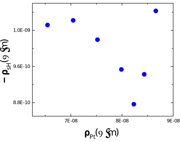
Fig. S5. Spin Hall resistivity versus total resistivity in Pt (6.3 µΩcm). The behavior (observed for both Pt films) clearly highlights the non-monotonic behavior of the SHA as well, and thus cannot be modeled with the simple linear equation.
Purely extrinsic spin Hall conductivity
Consider a sample where skew scattering, with impurities and with phonons, is the only source of the spin Hall effect. One solves the kinetic equation looking for the z-polarised spin current flowing along y, Jyz, in response to an electric field Ex. This yields
Jyz =τ
πN0v0
τi − 3πΛgN0T τph
(λpF)2
4 σDEx (4)
where 1/τ = 1/τi+ 1/τph is the scattering rate due to electron-impurity (1/τi) and electron- phonon (1/τph) scattering, λ an effective spin-orbit coupling constant, N0 the density of states at the Fermi energy, v0 the spatial average of the impurity potential (≈ 1/2N0 for a Thomas-Fermi-screened impurity), g and Λ respectively the electron-phonon and phonon-
4 . 0 E - 1 5 6 . 0 E - 1 5 8 . 0 E - 1 5 8 . 8 E - 1 0
9 . 6 E - 1 0 1 . 0 E - 0 9
r 2
P t ( Ω2 m 2
) - r sH(Ωm)
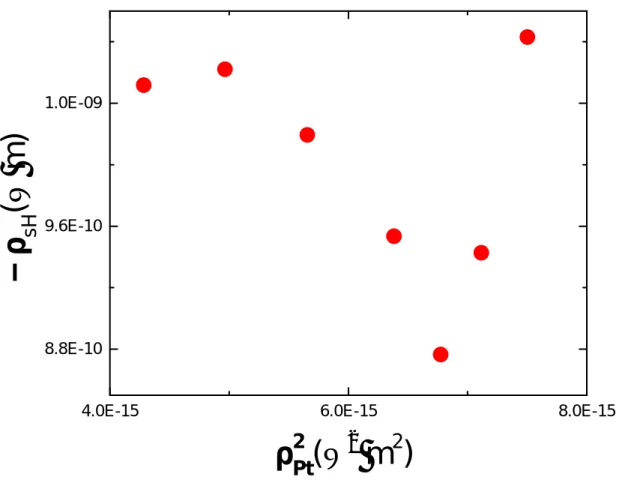
Fig. S6. Spin Hall resistivity versus the square of the total resistivity in Pt (6.3 µΩcm). The behavior (observed for both Pt films) again highlights the non-monotonic behavior of the SHA, and thus cannot be modeled with the quadratic equation either.
phonon coupling constants, and σD the Drude conductivity eN0vF2τ (notice the lack of e2, since we are dealing with spin, and not charge, currents). From the above one can write the skew scattering spin Hall conductivity as
σsHss = πN0v0 1 +τi/τphσD
1 + 3γ
2π(2πa/λF)3/2
| {z }
C2∼ O(1)
τi/τph T F
(λpF)2
4 . (5)
The ratio τi/τph = [ρ(T)−ρimp]/ρimp is accessible by simply measuring ρ(T) and looking at its residual T = 0 value ρimp. The numerical factor C2 is positive and can be roughly estimated as being of order 1 (herea is the distance between ions, while γ is the Gr¨uneisen
0 5 0 1 0 0 1 5 0 2 0 0 2 5 0 3 0 0
468
1 4 0 1 5 0 1 6 0 1 7 0 1 8 0
P t T a
r (µΩcm)
T e m p e r a t u r e ( K )
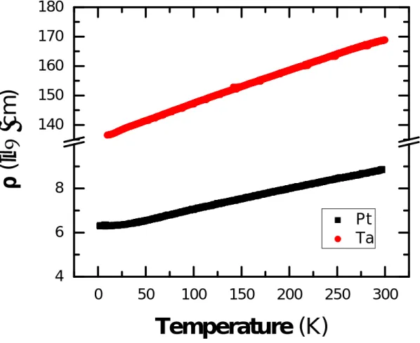
Fig. S7. Resistivity of Pt (6.3 µΩcm) and Ta (137 µΩcm) thin films measured as a function of temperature. They are found to behave linearly as expected in the 50−300 K temperature regime probed for the spin orbit torques.
parameter, typically≈3). In the T →0 limit one obtains σss,0sH =πN0v0(λpF)2
4
| {z }
C1
σimp (6)
showing the known result that skew scattering from impurities is proportional to theT = 0 conductivity σimp= 1/ρimp. It is possible to rewrite Eq. (5) as
σsHss = C1 ρ2
ρimp+C2 T
F ρ−ρimp
. (7)
When the temperature grows, the spin Hall conductivity decreases reaching a constant asymptotic value at T → ∞. The flattening of the curve takes place at a temperature T2
defined by
ρimp =C2T2 F h
ρ(T2)−ρimpi
(8) which implies that phonon skew scattering starts dominating over impurity skew scattering.
T2 is of the order of room temperature, but the precise value ofC2 depends on many material parameters and cannot be accurately estimated.
Adding an intrinsic contribution
One can introduce a temperature-independent intrinsic contribution σsHint. Assuming as usual that extrinsic and intrinsic channels work in parallel, σsH =σsHss +σsHint, this yields the full spin Hall conductivity
σsH =σintsH +C1 ρ2
ρimp+C2T
F ρ−ρimp
(9) and resistivity
ρsH ≈ −σsHρ2 =−σsHintρ2−C1
ρimp+C2T
F ρ−ρimp
. (10)
Contact with Eq. (4) in the main manuscript is established identifying θsHss,imp =C1, θss,phonsH (T) = C1C2 T
F θint,0sH =σsHintρimp ≡C3. (11) Scenario I: Clean sample
Consider a sample with very low residual resistivity, such that
C1 > C3 >0, (12)
having assumed positive C1, C3 to be definite (the same will be done in the following). The SHA starts byC1+C3 at zero temperature, and has to reach a minimum at T ≈T1, defined by
C1ρimp
ρ(T1) =C3ρ(T1). (13)
Beyond T1 an increase with (asymptotic) slope ∝ C3 sets in. This lasts roughly until the temperatureT2is reached, see Eq. (8). From this point on phonon skew scattering dominates impurity skew scattering, and the SHA slope increases by a factor ∝ C1C2. In a standard
metal like Pt one expectsT2 > TD, but nothing precise can be said unless an accurate value forC2 is given – this requires precise knowledge of both electron-phonon and phonon-phonon interaction strength. On the other hand, T1 < TD is likely, as T1 is set by the ratioC1/C3, which are both T = 0 properties of the sample.
Scenario II: Dirty sample
When the residual resistivity is higher, so that
0< C1 < C3, (14)
the SHA has a much simpler, monotonic temperature behaviour: it increases with (asymp- totic) slope ∝ C3 up to T2, where the steepness increases by a factor ∝ C1C2. Once more, without accurate knowledge of the various material parameters the precise behavior cannot be given. Indeed, in a certain parameter range the decrease of the extrinsic term and the increase of the intrinsic one could compensate each other over a certain temperature range, yielding a constant SHA therein.
Remarks on low temperatures
While phonon skew scattering has to vanish for T → 0, the exact form of the approach to zero is not yet known. This is an open and interesting subject for future research, which however does not change the qualitative discussion above.
∗ cosimo.gorini@physik.uni-regensburg.de
† now at: DGIST Research Center for Emerging Materials, DIGST, Daegu, 42988, Republic of Korea
‡ klaeui@uni-mainz.de
[1] L. van der Pauw, Philips Res. Rep. 13, 1 (1958).
[2] U. H. Pi, K. W. Kim, J. Y. Bae, S. C. Lee, Y. J. Cho, K. S. Kim, and S. Seo, Appl. Phys.
Lett.97, 162507 (2010).
[3] K. Garello, I. M. Miron, C. O. Avci, F. Freimuth, Y. Mokrousov, S. Bl¨ugel, S. Auffret, O. Boulle, G. Gaudin, and P. Gambardella, Nat. Nanotechnol.8, 587 (2013).
[4] M. Hayashi, J. Kim, M. Yamanouchi, and H. Ohno, Phys. Rev. B89, 144425 (2014).
[5] C. Gorini, P. Schwab, R. Raimondi, and A. L. Shelankov, Phys. Rev. B82, 195316 (2010).
[6] R. Raimondi, P. Schwab, C. Gorini, and G. Vignale, Ann. Phys. (Berlin)524, 153 (2012).
[7] C. Gorini, U. Eckern, and R. Raimondi, Phys. Rev. Lett. 115, 076602 (2015).