arXiv:1401.1955v2 [cond-mat.mes-hall] 14 Apr 2014
Martin Drienovsky,∗Franz-Xaver Schrettenbrunner, Andreas Sandner, Dieter Weiss, and Jonathan Eroms Institut f¨ur Experimentelle und Angewandte Physik, Universit¨at Regensburg, 93040 Regensburg, Germany
Ming-Hao Liu (劉明豪), Fedor Tkatschenko, and Klaus Richter Institut f¨ur Theoretische Physik, Universit¨at Regensburg, 93040 Regensburg, Germany
(Dated: April 15, 2014)
We report on transport properties of monolayer graphene with a laterally modulated potential profile, em- ploying striped top gate electrodes with spacings of 100 nm to 200 nm. Tuning of top and back gate voltages gives rise to local charge carrier density disparities, enabling the investigation of transport properties either in the unipolar (nn′) or the bipolar (np′) regime. In the latter, pronounced single- and multibarrier Fabry-P´erot (FP) resonances occur. We present measurements of different devices with different numbers of top gate stripes and spacings. The data is highly consistent with a phase coherent ballistic tight binding calculation and quantum capacitance model, whereas a superlattice effect and modification of band structure can be excluded.
I. INTRODUCTION
As one of the most exciting topics in condensed mat- ter physics1, monolayer graphene (MLG) provides a unique combination of striking mechanical, as well as electronic properties, such as the zero gap energy spectrum and lin- ear dispersion of charge carriers (Dirac fermions), leading to the half-integer quantum Hall effect2,3or relativistic phe- nomena on a mesoscopic scale (Klein tunneling4–6, electron lensing7). In recent years, there has been a vivid discus- sion on the issue of transport through bipolar junctions giv- ing rise to some thought provoking theoretical approaches8–11 and experiments12–14. Consequently, different intriguing sit- uations such as Klein tunneling and collimation at a single pn-junction or transmission through a bipolar barrier in the ballistic regime have been covered in scientific publications and revealed resonant behavior of conductance in analogy to optical Fabry-P´erot (FP) cavities15–17.
Taking a step further, efforts have been taken to investigate the concept of superlattices18for graphene, employing artifi- cial regular inhomogeneities to the monolayer, experimentally attainable either by gating or doping. For one-dimensional pe- riodic potentials in graphene, theory predicts conductance os- cillations corresponding to the emergence of additional Dirac points and the appearance of van Hove singularities in the den- sity of states19–22. Another experimental approach towards superlattices are hexagonal boron nitride (hBN)/graphene het- erostructures, where a moire pattern leads to an artificial band structure23.
Here we focus on the former approach, addressing finite multibarrier systems24. Ballistic transmission over a cou- ple of periods is essential for the observation of an artificial band structure. This is why the mean free path and phase coherence length of the charge carriers drastically limit the effect of a superlattice and samples with high charge carrier mobilityµ are needed. Recent works on high-µsuspended graphene devices25–27, implementing a single, tunable pn- junction, show stunning resonant behavior. With respect to multiple lateral barriers, suspended graphene is not a viable approach, as the large distance between the graphene-layer and the (buried) gate electrodes causes a significant smooth-
ing of the junction potential.
In order to overcome the problem of blurred potential steps and to provide a locally sharp potential profile at the bipolar junctions, an array of narrow electrode stripes on top of a thin dielectric, as has been introduced for a single bipolar ballis- tic potential barrier15, is suitable. We focus our research on locally gated graphene with varying number of bipolar barri- ers and different spacing in order to characterize the impact of changing parameters on the resistance of the monolayer.
A recent publication on a similar lateral multibarrier setup28 attributes the occurring resonant behavior of the resistance in the bipolar regime to a superlattice effect in the low-diffusive limit, even though the experimental elastic mean free path does not exceed one lattice period. We reproduce the reported resonant features and provide extended data for varying exper- imental parameters that can be explained within a consistent Fabry-P´erot resonance model, without resorting to a superlat- tice effect.
II. ELECTRONIC TRANSPORT THROUGH MULTIBARRIERS IN GRAPHENE
A. Device fabrication
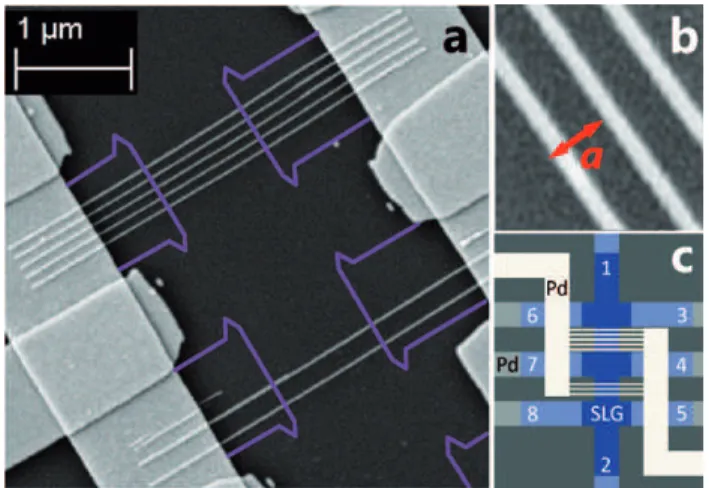
Here we present devices where graphene has been exfoli- ated micromechanically on SiO229 (devices A and R), or al- ternatively, transferred on a hBN30/SiO2substrate (device B) using a PVA/PMMA based method similar to Ref.31. Hall- bars were etched with O2/Ar (50:50) plasma at 30 mTorr and 50 W. Al2O3was used as a top gate dielectric, built up by a thin film of electron beam evaporated and oxidized aluminum, serving as a thin seed-layer for the following atomic layer de- position (ALD). In total, the top gate oxide does not exceed a height of 15 nm. The contacts and the patterned top gate elec- trode were exposed by electron beam lithography and electron beam evaporation of Pd. Experiments were carried out using an ac lock-in four point measurement setup in a4He cryostat
(T=1.3. . .200 K) and Bmax=14 T. Figure1depicts the de-
vice geometry.
We focus on data of three samples that provide regions with
FIG. 1. Device geometry. SEM image (a) of device B with 5 and 2 top gate stripes. The graphene hallbar is buried under the dielectric, here visualized by the violet contour. Zoom-in (b) of the locally gated area of three Pd stripes of device A (region A3) with a pitch of aA3= 100 nm. (c) Schematic of the sample geometry of all devices used in this publication employing a MLG hallbar (blue), contacted by a 40 nm thick Pd fine wiring (light grey). The width of the transport channel is 1µm, as well as the spacing of the labeled voltage probes.
The striped Pd top gate electrode of 15 nm height and the top gate leads (white) are separated from the graphene by a∼15 nm thin Al2O3dielectric.
different numbers of top gate stripes and spacing (in the fol- lowing A3, A5, B2, B5, R8, labels corresponding to number of top gate stripes) and compare them to our ballistic transport simulation.
B. Electronic Transport 1. Preliminary considerations
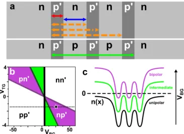
Using both the planar Si++back gate and the patterned Pd top gate electrode, the charge carrier density can be tuned both locally and globally and hence an array of potential barriers is created. Fig. 2(a) shows a schematic of the Fabry-P´erot cavities in the exemplary multibarrier system of three-striped sample region A3. For simplicity, we address the graphene cavity under the top gate stripes as “barrier”, the one between neighboring top gates as “well”. The region without top gate is referred to as the “ungated” area, that is the area between the gated region of barriers and wells and the probe contacts of the Hall bar. The regions of different charge carrier densities are depicted by different grayscale in the figure.
In the fully phase coherent bipolar transport regime of Fig.
2(a), Klein-collimation yields an increase of reflectivity for obliquely incident charge carriers at the multiple pn or np junctions, hence, the finesse of the cavities is greatly in- creased. The reflections in the barrier cavities are highlighted with a red arrow, the ones in the wells are marked blue. The possible reflection traces kept in orange are less relevant due to high reflectivity of the bipolar junctions in the transmission path for oblique incidence. The green trace (i.e. the interme-
diate regime, see below) is more important to note due to a mismatch of potential in the gated area and the ungated area, as can be explicitly seen in the sketched corresponding charge carrier density profile in Fig.2(c). This difference can be at- tributed to the impact of the top gate stripes on the well area due to electric field broadening. The oscillations in this larger cavity will play a role later on when we come to explain the difference between measurement and simulation.
Plotting the resistance with respect to top- and back gate voltage yields four quadrants, depending on different combi- nations of charge carrier concentration of barriers, wells and ungated area [Fig.2(b)]. The schematic color map features an hourglass-shaped pattern of high resistance, that in general can be attributed to high resistivity of the bipolar pn′ or np′ junctions of the gated area, where the primed charge carrier concentrations stand for the area under the top gate stripes, the unprimed ones for the well areas, respectively. This re- gion of bipolar transport is coarsely depicted by purple and will be analyzed for the case of ballistic transmission later on in more detail. The white areas of the color map stand for the unipolar pp′or nn′low resistance transport regime, where the barrier and well charge carrier concentrations are of the same sign. The narrow green area of higher resistance is an inter- mediate bipolar regime, where the gated area is still unipolar, but already enclosed by the ungated area of different charge polarity.
In Fig.2(c) we address the different situations of the color map and plot schematics of the charge carrier density profiles n(x)with respect to charge neutrality. The black curve stands for the unipolar regime, where a negative top gate voltage cre- ates a modulation of the potential profile. Note the exagger- ated mismatch of carrier density heights in the gated and un- gated area. Now following the black dotted cut in the color map of Fig.2(b) by increasing the global back gate voltage from negative values towards positive ones, the carrier den- sity is moved upward until it fulfills the charge neutrality con- dition for the ungated area. That is the bold black vertical line in the color map, separating the unipolar and bipolar regime.
For pristine or homogeneously doped MLG, this line of neu- tral charge should intersect with the Dirac point of the locally gated area, that is the center of the hourglass pattern where the dark green and dark purple border lines intersect.
Further increase of voltage induces electrons as charge car- riers in the ungated area and one enters the narrow interme- diate regime [green curve in Fig.2(c) and green area of Fig.
2(b), respectively], followed by another crossing (dark green diagonal line of the colorplot). That is the charge neutral- ity line of the wells, separating the intermediate and bipolar regime. Another increase lifts the modulated potential into the bipolar regime, where the charge carriers in the barriers and in the wells are of different sign [light purple curve and area respectively, same situation as in Fig.2(a)]. A raise of back gate voltage finally leads to the crossing of the barrier charge neutrality line, that is the dark purple line of the color map, where the back- and top gate induced displacement fields cancel each other and the charge carrier density is minimal un- der the stripes. Concluding the trip following the dotted line, one ends up in the unipolar nn′ situation, where the overall
charge carrier density modulation is still unchanged, whereas the charges in barrier and well are of the same sign again.
FIG. 2. Resonances and resistance behavior in a graphene multi- barrier system. (a) Schematic of the Fabry-P´erot cavities in the multibarrier system of sample A, region A3 in the bipolar and in- termediate regime, respectively. Increased reflectivity for ballistic charge carriers in the bipolar regime yields resonances (colored ar- rows) at the pn junctions. (b) Sketch of the expected resistance hourglass-like pattern for the samples presented in this paper, where the different colors stand for the different transport regimes. The primed letters stand for the charge carriers in the barrier, the unla- beled for those in the well of the lattice. The bold black line depicts the charge neutrality line (Dirac point) of the area without top gate.
The dark green line stands for the charge neutrality line of the wells and the dark purple for the one of the barriers. The green area is de- noted as intermediate bipolar regime in the text. The black star points out the situation shown in (a). The schematic of according charge carrier density is shown in (c), where the three different regimes are plotted with respect to charge neutrality.
2. Transport measurement on device A
The mobility of sample A is approximately 7000 cm2V−1s−1, following a standard capacitor model. This im- plies a mean free path for charge carriers lm, exceeding the effective bipolar barrier width, as well as the effective well width (e.g. lm≈100 nm at VBG=20 V), so that transport is ballistic over one stripe, but not over the entire lattice.
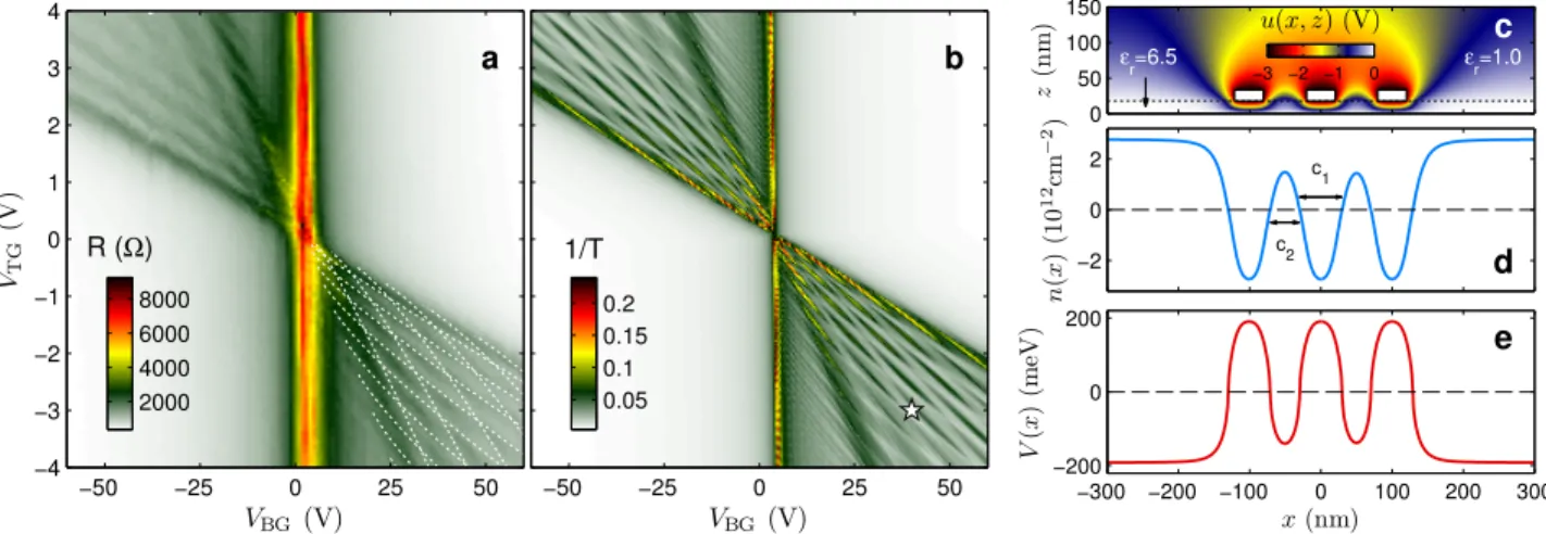
Figure3(a) shows one of the main results of this work, the color-coded resistance map of region A3 with respect to the two gate voltages. The four-point resistance RA3is taken from the voltage drop across the multibarrier region A3 with a pitch of aA3=100 nm. The relatively large free space between the locally gated area and the probe contacts yields an intense, vertical, top gate-independent resistance maximum (R≈10 kΩat VBG=3 V), that is the Dirac point of the ungated area.
In the bipolar transport regime, pronounced resistance oscilla- tions, coming from barrier and well resonance, form the afore- mentioned hourglass-like pattern. The white dashed lines in the lower right quadrant refer to oscillations originating in
these two different cavities and will be addressed in Sec. II B 4 in more detail. The dark diagonal charge neutrality line of the well area is clearly observable and separates the os- cillating bipolar region from the narrow intermediate bipolar region [cf. green area of Fig.2(b)]. Unlike the ungated area around the leads, where the charge carrier density is solely controlled by the back gate voltage, the top gate additionally influences the potential of the well area due to effective elec- tric field broadening, coming from electrostatic edge effects at the Pd electrode stripes. This leads to the intermediate situa- tion, where the polarity of barrier and well is similar, but the one of the ungated area is already different.
Note also, that the capacitive coupling of the top gate com- pared to the back gate for both locally gated areas A3 and A5 of device A is 26-times higher, which can be attributed to high ratio of dielectrics thickness and disparity in dielectric constant of the two oxides.
3. Transport simulation
To identify the source of the Fabry-P´erot interference pat- terns observed in Fig. 3(a), ballistic transport calculations were performed using the Green’s function formalism in the phase coherent, clean limit. Following the SEM image of the region A3 shown in Fig.1, we consider a tight-binding model Hamiltonian (with hopping strength t),
H0=−t
∑
hm,ni
c†mcn (1)
for a 1µm wide and 600 nm long armchair graphene ribbon.
The summation in Eq. (1) runs over all the lattice site indices that are nearest neighbors to each other,hm,ni. The diago- nal elements of the model Hamiltonian are modulated by a realistic local energy band offset profile that is linked to the experimental parameters of gate voltages. For simplicity, we assume such a band offset profile to vary only with coordinate x along the transport direction, and perform two-dimensional (x-z) electrostatic simulation to obtain the carrier density pro- file n(x), from which, combined with the quantum capacitance model,32,33the gate-dependent energy band offset profile V(x) can then be deduced.
Instead of fully taking into account the Hall bar struc- ture used in the 4-point measurement, we simplify the trans- port problem to a 2-terminal structure, which is proved to be enough to capture the main experimentally observed features.
Hence together with the self-energiesΣL andΣR due to the coupling to the left and right leads, the full model Hamilto- nian reads
H=H0+
∑
n
V(xn)c†ncn+ΣL+ΣR, (2) where the summation runs over all the lattice site indices and xnis the x-coordinate of the nth lattice site.
With the model Hamiltonian (2), the transmission function T is computed by the recursive Green’s function method.34 Figure3(b) shows the inverse of the calculated transmission function, which agrees qualitatively well with the measured
VBG (V) VTG(V)
a
−50 −25 0 25 50
−4
−3
−2
−1 0 1 2 3 4
R (Ω)
2000 4000 6000 8000
VBG (V)
b
−50 −25 0 25 50
1/T
0.05 0.1 0.15 0.2
z(nm)
ε
r=6.5 ε
r=1.0
c
0 50 100
150 u(x, z) (V)
−3 −2 −1 0
n(x)(1012cm−2)
c1
c2
d
−2 0 2
V(x)(meV)
x(nm)
e
−300 −200 −100 0 100 200 300
−200 0 200
FIG. 3. Resonance pattern in the bipolar regime. Color-coded plot of (a) the four point resistance for region A3 with w≈25 nm stripe width and aA3≈100 nm periodicity, and (b) the inverse of the calculated transmission function in fully phase coherent limit. A pronounced resistance pattern occurs in the bipolar regime, arising from superposition of barrier and well resonance. (c) Electrostatic simulation for the top gate contribution to the carrier density in graphene, which locates at z=0, at VTG=−3 V as an example. Together with the uniform contribution from the back gate set to be VBG=40 V as an example [(VBG,VTG) = (40,−3)V point is marked by the white star in (b)], the carrier density profile and the corresponding local energy band offset profile are sketched in (d) and (e), respectively. The white dashed lines sketched in (a) are resonant voltage contours VTGres,j(VBG)and VBGres,j(VTG)obtained by numerically solving Eq. (3) for cavity c1and c2[marked in (d)], respectively; see text.
resistance map shown in Fig.3(a). Such a good agreement re- lies closely on the optimal electrostatic model that generates the correct gate voltage dependence of the local energy band offset applied to the diagonal elements of the model Hamil- tonian. The geometry of the adopted electrostatic model is sketched in Fig.3(c).
To obtain a close match between the experimental results and the numerical simulations, the oxide thickness and Pd stripe width (fabrication design values 15 nm and 25 nm, re- spectively) were slightly modified to 18 nm and 40 nm, re- spectively. Note also that the back gate contribution is as- sumed to be uniform, so that the standard capacitor model can be used. Furthermore a uniform p-type chemical doping concentration of n0=−2×1011cm−2is considered, which is deduced from the slightly shifted Dirac point in the ungated region [vertical thick line in Fig.3(a)].
For details about simulating the gate-induced carrier den- sity in graphene, see, for example, Ref. 35for a tutorial in- troduction using thepdetool36 of MATLAB. Alternatively, one can as well choose the free automated finite element simulator–the FEniCS project,37which is adopted, combined with the free mesh generator–GMSH,38in the present work.
4. Analysis on the Fabry-P´erot interference patterns Figures3d and e illustrate as an example the carrier den- sity profile n(x)and the corresponding energy band offset pro- file V(x), respectively, at gate voltages(VBG,VTG) = (40,−3) V, as marked by the white star in Fig.3b. We next attribute the different set of Fabry-P´erot interference patterns to the resonance in specific cavity regions. For this, we first label the cavity under the top gate (barrier) c1, and the region be-
tween two neighboring top gates (well) c2. Taking the n(x) sketched in Fig.3d for example, we may regard c1as the re- gion−30 nm.x.30 nm and c2as−70 nm.x.−30 nm.
Within cavity ci, the resonance condition can be qualitatively written as
2 Z
ci
pπ|n(x)|dx=2 jπ, j=1,2,· · ·, (3)
wherep
π|n(x)|=kF(x)is the position dependent wave num- ber. The left hand side of Eq. (3) can be understood as the phase difference between directly transmitted and twice re- flected electron waves. When such a phase difference is an integer multiple of 2π, constructive interference is expected.
Since n(x), and hence the cavity size, vary with the gate voltages, Eq. (3) has to be solved numerically. At a fixed back gate voltage, there exists a discrete number of top gate volt- ages that satisfy the resonance condition (3) when solving for the cavity c1. Sweeping the back gate voltage in the bipo- lar range, one obtains the resonant top gate voltage contours as a function of back gate voltage, VTGres,j(VBG), which form a group of lines that are roughly parallel to the diagonal charge neutrality line of the barriers, that is the dark purple bound- ary discussed in Fig.2(b). Likewise, one can solve Eq. (3) for the cavity c2 to obtain VBGres,j(VTG)contours, which form a group of lines roughly parallel to the steep, dark diagonal charge neutrality line of the wells, shown in Fig.3(a) or (b), also schematically depicted by the dark green border in Fig.
2(b).
Sketching the VTGres,j(VBG)and VBGres,j(VTG)contours on the resistance map of Fig.3(a) (inset of dashed white lines), we find a very good agreement of the periodicity of the interfer- ence patterns. This enables us to correctly attribute the differ-
ent origins of the different sets of interference patterns to the resonance in different cavities c1(barrier) and c2(well).
5. Discussion
Despite the good agreement between the measurement [Fig.
3(a)] and simulation [Fig.3(b)], a closer look at the latter in- dicates that the interference patterns in the ideal calculation are more complicated and more pronounced than the former in the bipolar regime due to phase coherence assumed over the whole area. Addressing the cavity picture of Fig.2(a), the fringes result primarily from superposition of barrier- (red) and well resonance (blue). Moreover, the simulated map of Fig.3(b) shows fringes with a shorter oscillation period, aris- ing in the intermediate region. These can be traced back to resonances in a larger cavity [cf. green trace in Fig.2(a)]. In the experiment, we are not able to see the short period oscil- lations in this particular region due to the fact that the length of the intermediate cavity exceeds the mean free path of the sample. Instead, a blurred area of higher resistance is ob- served and can be attributed to diffusive transmission in the intermediate bipolar regime.
In order to get an insight into the role of a finite mean free path and phase coherence length, we successively reduced the number of barriers in the simulation, while retaining the mis- match of inner and outer well potential (not shown). Compar- ing the measured and simulated resistance plot qualitatively, we estimate the ballistic length to 1.5 times the effective bar- rier width, as only the oscillations coming from barrier reso- nance are clearly pronounced [Fig. 3(a)]. Evidently, ballistic transmission in the range of the barrier width is essential to evoke resistance oscillations, on the other hand, phase coher- ence over the whole top gated area is not required to repro- duce the general behavior. Hence, the multibarrier system can be understood as independent FP cavities stringed together, giving rise to a single barrier pattern in the locally ballistic limit.
C. Devices B and R
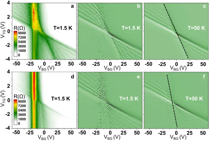
Next, we discuss device B, that shows similar behavior to device A with respect to mobility (µB ∼6300−8300 cm2V−1s−1) and resonance pattern [Fig. 4]. The top gate voltage-independent charge neutrality line of the ungated area though does not coincide with the ones of the hourglass-like pattern of B5 [Fig.4(a)]. The ungated region appears to be n-doped (DP at VBG=−20 V, whereas the top gated zone B5 shows a lower dopant level (DP for VTG=0 V at VBG=−4 V). Interestingly, this inhomogeneity is consistent for both top gate areas, B2 and B5, that are spatially separated and thus the inhomogeneity can only be attributed to some preparation step of the top gate oxide and electrodes that changed the intrinsic doping at the different sites. Keep in mind that the spacing between the top gate stripes of the regions B2 and B5 is dif- ferent, aB2=200 nm and aB5=100 nm, whereas the width
of the top gated area (barrier) is similar≈25 nm [cf. SEM- picture in Fig.1(a)].
The impact of the top gates on the charge carrier density in the region between two stripes is lower for region B2 and therefore the potential mismatch of the well and ungated re- gion is smaller. This results in different slopes of the well charge neutrality lines in the resistance maps [dashed slopes in Fig.4(c) and (f)]. One can assume, that for the larger well cavity of B2 (where aB2>lm), ballistic interference is sup- pressed. On the other hand, one can expect a superposed res- onance pattern of barrier and well cavities for B5, as aB5.lm, similar to sample A3. Fig.4(b) shows the numerical derivative of the resistance pattern of B5 with respect to the top gate volt- age. In this plot, superposition of resonances can be resolved, but the bright charge neutrality line of the ungated region is filtered. The derivative of the resistance in region B2 [Fig.
4(e)] only features the pronounced parallel resonance peaks coming from single barrier resonance.
FIG. 4. Resistance ocillations of sample B. (a) Color map of resistance in region B5 (five stripes) and its derivative with respect to the top gate voltage (b). A pattern with barrier and well resonance contribution is observable, the vertical charge neutrality line of the ungated area is filtered. (c) At T=50 K, the superposition fades out and one obtains a softened single barrier resonance pattern. Similar data for region B2 is plotted in (d)-(f).
FIG. 5. Temperature dependence and resistance oscillation pe- riod of sample B, (a) Temperature development of a top gate sweep.
Sweep performed at a back gate voltage VBG=−40 V in region B5.
The curves are offset by 500Ωfor clarity. (b) Comparison of the oscillation periods∆nTGfor sample regions B5 and B2 for top gate voltage sweeps at different back gate voltages at 20 K.∆nTGis the average spacing between two resistance peaks of a single top gate sweep as depicted in (a), with respect to change in charge carrier density.
We performed temperature-dependent measurements on device B and find that the FP oscillation amplitude is decreas- ing with higher temperatures T [cf. Fig.5(a)]. As expected, the period of resistance oscillation with respect to charge car-
rier density remains unchanged. The features originating from superposition of barrier and well resonance at 1.5 K are suc- cessively suppressed at higher T that is due to temperature activated dephasing and loss of ballistic transmission. As the phase coherence length decreases with T , only the single bar- rier resonance survives, resulting in a softening of the resis- tance pattern.
Comparison of different top gate voltage sweeps at 20 K for regions B5 and B2 [Fig.5(b)] yields that the oscillation period of the remaining pronounced resonance fringes with respect to the charge carrier density is pretty similar for both regions.
This, together with the fact that the resonance pattern remains observable at higher temperatures, clearly proves local ballis- tic Fabry-P´erot interference originating in the barriers.
Finally we briefly discuss our last sample R. Again, the electronic properties are very similar to the other two devices A and B, however it has been fully covered by a lateral top gate electrode array of 200 nm lattice constant. In Fig.6(a), we observe pronounced FP oscillations at T =1.5 K for a sample region of 8 stripes (R8). While the large steps in VBG do not allow resolving the fine structure of this pattern, we once again recognize the characteristic hourglass shape in Fig.6(b), but do not encounter the intermediate bipolar regime
FIG. 6. Resistance oscillations of sample R8. R8 has been fully covered by top gate stripes (aR8=200 nm) and shows for a sample area of 8 stripes similar behavior to devices A and B. The resistance of single top gate sweeps at different back gate voltage and at T=1.5 K (a) feature clear oscillations. The resistance map shows the general hourglass-like pattern, separating the map into four quadrants (b).
[green area in Fig.2b], as it is exclusive to devices A and B with local gating. Here, the top gate electrode lattice covers the whole transport channel. Hence, there is no area without top gate stripes and the potential shows no mismatch in this case.
D. Towards superlattices
The analysis of our data lets us finally conclude that there is no evidence of an artificial band structure and thus a superlat- tice effect in our multibarrier system. This stands in contrast to the argumentation of Ref. 28, where a similar device with an even higher number of top gate stripes was investigated.
Our calculations for a fully phase coherent system of NTGtop gate stripes yield growing of resistance peaks due to the for- mation of new touching points of valence and conductance band as the band structure gets folded, giving rise to the open- ing of small energy band gaps. In the FP picture, in the case of only a few periods, the destructive interference gives rise to these resistance peaks and these peaks do not exceed the one at the usual Dirac point. This is consistent with all data extracted from our samples. In Figs.7(a)-(d) we plot the cal- culated inversed phase coherent transmission of a back gate sweep at VTG=3 V for various numbers of top gate stripes, showing a global Dirac point at VBG≅−2 V. When NTGex- ceeds∼10, the heights of the resonance peaks start to be of the same order or even higher than that of the usual Dirac point. One should see the resistance at those anti-crossings as diverging in comparison to that at the usual Dirac point, however, the miniband structure should be extremely sensi- tive to inhomogeneity. This is why the mean free path and
phase coherence length appear to be a limiting factor for the emergence of mini band gaps and diverging resistance peaks.
Hence a combination of high-mobility graphene on a substrate (i.e. hBN/graphene heterostructures) and small top gate lattice periods seems to be the most obvious option in order to pave the way to sizable superlattice effects in graphene.
0 10 20 30
1/T
NTG= 2 a
0 10 20 30
1/T
NTG= 5 b
−400 −20 0
20 40
VBG(V)
1/T
NTG= 10 c
−40 −20 0 0
50 100 150
VBG(V)
1/T
NTG= 40 d
FIG. 7. Impact of superlattice on a fully phase coherent graphene system. The figures (a)-(d) depict the calculated inversed transmis- sion for a single back gate sweep for different numbers of barriers NTG. The peak of the original Dirac point occurs at VBG≅−2 V and, with increasing NTG, gets surpassed by resistance peaks origi- nating in destructive interference.
III. CONCLUSION
In summary, we fabricated top gated graphene multibar- rier systems with different number of bipolar potential bar- riers and spacing. We observe highly pronounced resistance oscillations in the bipolar transport regime in each of our de- vices, which can be attributed to Fabry-P´erot resonance in the ballistic limit of one barrier or well length. In the locally gated samples, we encounter three charge neutrality lines that come from different potentials in the gated and ungated ar- eas. Moreover, we consistently reproduced our measurements in a transport simulation, employing a realistic potential pro- file, extracted from electrostatics and a quantum capacitance model.
ACKNOWLEDGMENTS
Financial support by the Deutsche Forschungsgemeinschaft (DFG) within the programs GRK 1570 and SFB 689 and by the Hans B¨ockler Foundation (F.T.) is gratefully acknowl- edged.
∗ martin.drienovsky@physik.uni-regensburg.de
1 K. S. Novoselov, V. I. Fal’ko, L. Colombo, P. R. Gellert, M. G.
Schwab, and K. Kim, Nature 490, 192 (2012).
2 K. S. Novoselov, A. K. Geim, S. V. Morozov, D. Jiang, M. I.
Katsnelson, I. V. Grigorieva, S. V. Dubonos, and A. A. Firsov,
Nature 438, 197 (2005).
3 K. S. Novoselov, Z. Jiang, Y. Zhang, S. Morozov, H. Stormer, U. Zeitler, J. Maan, G. Boebinger, P. Kim, and A. Geim, Science 315, 1379 (2007).
4 O. Klein, Z. Phys. 53, 157 (1929).
5 N. Dombey and A. Calogeracos, Phys. Rep. 315, 41 (1999).
6 M. I. Katsnelson, K. S. Novoselov, and A. K. Geim, Nat. Phys.
2, 620 (2006).
7 V. V. Cheianov, V. Fal’ko, and B. Altshuler, Science 315, 1252 (2007).
8 V. V. Cheianov and V. I. Fal’ko, Phys. Rev. B 74, 041403 (2006).
9 L. M. Zhang and M. Fogler,Phys. Rev. Lett. 100, 116804 (2008).
10 A. V. Shytov, M. S. Rudner, and L. S. Levitov, Phys. Rev. Lett.
101, 156804 (2008).
11 D. A. Abanin and L. S. Levitov, Science 317, 641 (2007).
12 R. V. Gorbachev, A. S. Mayorov, A. K. Savchenko, D. W. Horsell, and F. Guinea, Nano Lett. 8, 1995 (2008).
13 B. ¨Ozyilmaz, P. Jarillo-Herrero, D. Efetov, D. A. Abanin, L. S.
Levitov, and P. Kim, Phys. Rev. Lett. 99, 166804 (2007).
14 J. Williams, L. DiCarlo, and C. Marcus, Science 317, 638 (2007).
15 A. F. Young and P. Kim, Nat. Phys. 5, 222 (2009).
16 N. Stander, B. Huard, and D. Goldhaber-Gordon, Phys. Rev. Lett.
102, 026807 (2009).
17 J. Pereira Jr, F. Peeters, A. Chaves, and G. Farias, Semicond. Sci.
Technol. 25, 033002 (2010).
18 L. Esaki and R. Tsu, IBM J. Res. Dev. 14, 61 (1970).
19 C.-H. Park, L. Yang, Y.-W. Son, M. L. Cohen, and S. G. Louie, Nat. Phys. 4, 213 (2008).
20 N. Abedpour, A. Esmailpour, R. Asgari, and M. R. R. Tabar, Phys. Rev. B 79, 165412 (2009).
21 L. Brey and H. Fertig, Phys. Rev. Lett. 103, 046809 (2009).
22 M. Barbier, P. Vasilopoulos, and F. Peeters, Phys. Rev. B 81, 075438 (2010).
23 M. Yankowitz, J. Xue, D. Cormode, J. D. Sanchez-Yamagishi, K. Watanabe, T. Taniguchi, P. Jarillo-Herrero, P. Jacquod, and
B. J. LeRoy, Nat. Phys. 8, 382 (2012).
24 R. Tsu and L. Esaki, Appl. Phys. Lett. 22, 562 (1973).
25 P. Rickhaus, R. Maurand, M.-H. Liu, M. Weiss, K. Richter, and C. Sch¨onenberger, Nat. Commun. 4, 2342 (2013).
26 A. L. Grushina, D.-K. Ki, and A. F. Morpurgo, Appl. Phys. Lett.
102, 223102 (2013).
27 M. Oksanen, A. Uppstu, A. Laitinen, D. J. Cox, M. Craciun, S. Russo, A. Harju, and P. Hakonen, arXiv: 1306.1212 (2013).
28 S. Dubey, V. Singh, A. K. Bhat, P. Parikh, S. Grover, R. Sensarma, V. Tripathi, K. Sengupta, and M. M. Deshmukh, Nano Lett. 13, 3990 (2013).
29 K. Novoselov, A. Geim, S. Morozov, D. Jiang, Y. Zhang, S. Dubonos, I. Grigorieva, and A. Firsov, Science 306, 666 (2004).
30 We used commercially available hBN powder.
31 C. Dean, A. Young, I. Meric, C. Lee, L. Wang, S. Sorgenfrei, K. Watanabe, T. Taniguchi, P. Kim, K. Shepard, et al., Nat. Nan- otech. 5, 722 (2010).
32 T. Fang, A. Konar, H. Xing, and D. Jena,Appl. Phys. Lett. 91, 092109 (2007).
33 M.-H. Liu,Phys. Rev. B 87, 125427 (2013).
34 M. Wimmer and K. Richter,J. Comput. Phys. 228, 8548 (2009).
35 M.-H. Liu,J. Comput. Electron. 12, 188 (2013).
36 Partial Differential Equation ToolboxT M User’s Guide, The MathWorks, Inc., matlab 2012a ed. (2012).
37 A. Logg, K.-A. Mardal, and G. N. Wells,Automated Solution of Differential Equations by the Finite Element Method (Springer, Berlin, Heidelberg, 2012).
38 C. Geuzaine and J.-F. Remacle, Int. J. Numer. Meth. Engng. 79, 1309 (2009).