Optics on materials with strong spin-orbit coupling:
topological insulators Bi2−xSbxTe3−ySey and the j = 1/2 compounds Na2IrO3 and α-RuCl3
Inaugural-Dissertation zur
Erlangung des Doktogrades
der Mathematisch-Naturwissenschaftlichen Fakult¨at der Universit¨at zu K¨oln
vorgelegt von Nick Borgwardt aus Berlin-Neuk¨olln
K¨oln 2019
Berichterstatter: Prof. Dr. Markus Gr¨uninger (Gutachter)
Prof. Dr. Paul H. M. van Loosdrecht
Tag der m¨undlichen Pr¨ufung: 19.06.2018
Contents
1 Introduction 1
1.1 Strong spin-orbit coupling . . . . 1
1.2 Outline . . . . 2
I Optical response of matter 3 2 Light as electromagnetic wave 5 2.1 Dielectric function . . . . 5
2.2 Linear response . . . . 7
2.3 Interfaces . . . . 9
2.4 Multilayer systems . . . . 11
2.5 Thin film . . . . 15
3 Models and relations 17 3.1 Lorentz oscillator . . . . 17
3.2 Drude oscillator . . . . 18
3.3 Tauc-Lorentz oscillator . . . . 19
3.4 Fano line shape . . . . 19
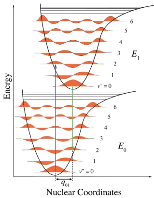
3.5 Franck-Condon principle . . . . 20
3.6 Kramers-Kronig relation . . . . 20
3.7 Maxwell Garnett approximation . . . . 21
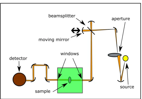
II Methods 23 4 Measuring instruments 25 4.1 FTIR spectrometer . . . . 25
4.2 THz spectrometer . . . . 27
4.3 Ellipsometer . . . . 27
5 Data analysis 29 5.1 Inverting transmittance and reflectance . . . . 29
5
7.1 Crystal structure and fundamental properties . . . . 47 7.2 Data and analysis for Bi2Te3 . . . . 51 7.3 Thin film of compensated (Bi0.57Sb0.43)2Te3. . . . 59
8 Compensated topological insulators 65
8.1 BiSbTeSe2. . . . 66 8.2 Bi2−xSbxTe3−ySey . . . . 94 8.3 Summary . . . 105
IV Spin-orbit-entangled Mott insulators 107
9 Introduction to spin-orbit-entangled Mott insulators 109 9.1 Mott insulators . . . 109 9.2 Hubbard model . . . 110 9.3 From spherical harmonics to the j= 1/2 groundstate . . . 110 10 Results on spin-orbit-entangled Mott insulators 125 10.1 4d5Mott insulatorα-RuCl3 . . . 125 10.2 Na2IrO3 . . . 140
V Appendix 151
Abstract
We performed temperature-dependent infrared transmittance and reflectance measurements on topological insulators and spin-orbit-entangled Mott insulators. Both material classes ex- hibit strong spin-orbit coupling which gives rise to topologically protected phases. Potential applications are hindered, due to various deviations of the synthesized crystals from the ideal topological insulator or spin-orbit-entangled Mott insulators, respectively. In this the- sis several promising candidates for the realization of either models are investigated.
For topological insulators the bulk conductivity poses a problem. We report on thickness- dependent data on thin films of Bi2Te3which show that the bulk optical conductivityσ1(ω) superimposes the surface conductance. Therefore, we continue the search for signatures of the surface state on compensated (Bi0.57Sb0.43)2Te3, for which we report on a very lowσ1(ω), but we find no direct evidence for the topologically protected surface state. The compen- sation of topological insulators can be performed more sophisticated by partly substituting Te with Se. Thereby, the family of topological insulators Bi2−xSbxTe3−ySey with insulating behavior is created. Nevertheless, compensated topological insulators have a reduced acti- vation energy compared to the intrinsic gap, which is usually attributed to impurity band.
Lately, the formation of charge puddles in compensated topological insulators, due to the random distribution of defects, thus reducing the activation energy, was predicted. We re- port on the experimental verification of charge puddles and reveal the highly non-monotonic temperature dependence of them. Additionally, we describe, in collaboration with the group of Prof. Rosch of the Institute for Theoretical Physics at the University of Cologne, the ob- servations semiquantitatively by Monte Carlo simulations. Thereby, we gain insight into, e.g., the defect density and the level of compensation depending on the composition which allows to choose the composition best suited the each purpose.
One of the thrilling phenomena in Kitaev physics is the occurrence of a quantum spin liquid in the ground state. However, finite Heisenberg exchange due to a trigonal crystal field or finite mixing of thet2g and eg states, causes deviations from purej= 1/2 states, which re- sults in a zigzag-ordered ground state instead of the sought-after quantum spin liquid. Due to these deviations even the formation of quasi-molecular orbitals instead of localj = 1/2 states was suggested for RuCl3 and Na2IrO3. We investigate σ1(ω) and identify different excitations, thereby gaining insight into the underlying physics. Inα−RuCl3 we reveal the single, double, and triple spin-orbit exciton. Hence, local j = 1/2 states are formed in this compound. For Na2IrO3 precise predictions on the optical spectrum depending on the underlying physics allow us to conclude fromσ1(ω) that the localj= 1/2 scenario is appro- priate. Furthermore, we report on signatures of a controversially discussed peak obtained by RIXS, in the optical spectrum including magnon sidebands.
gischen Oberfl¨achenzustand bei kompensierten topologischen Isolatoren BiSbTe weiter. F¨ur (Bi0.57Sb0.43)2Te3 finden wir sehr kleineσ1(ω), allerdings keine direkten Belege f¨ur topolo- gisch gesch¨utzt Oberfl¨achenzust¨ande. Die Kompensation von topologischen Isolatoren kann raffinierter betrieben werden, indem man Te teilweise mit Se ersetzt. Dabei erzeugt man die Familie der topologischen Isolatoren Bi2−xSbxTe3−ySey, die isolierend im Volumen ist.
Allerdings weisen kompensierte topologische Isolatoren eine kleiner Aktivierungsenergie im Vergleich zu ihrer Bandl¨ucke auf. Dies wird h¨aufig mit Defektb¨andern in Zusammenhang ge- bracht. Vor Kurzem wurde vorhergesagt, dass Pf¨utzen von Ladungstr¨agern in kompensierten topologischen Isolatoren entstehen, welche die reduzierte Aktivierungsenergie verursachen.
Wir konnten die Ladungstr¨ager Pf¨utzen experimentell nachweisen und beobachteten ihr stark nicht monotones Verhalten. Zus¨atzlich konnten wir, in Kollaboration mit der Gruppe von Prof. Rosch aus dem Institut f¨ur theoretische Physik der Universit¨at zu K¨oln, die Beobachtungen semiquantitativ durch die Monte-Carlo Simulation beschreiben. Dabei er- hielten wir Einblick in, z.B. die Defektdichte und den Grad der Kompensation, abh¨angig von der Zusammensetzung. Dies erlaubt es die richtige Zusammensetzung f¨ur die entsprechende Anforderung zu w¨ahlen. Eins der spannendsten Ph¨anomene der Kitaev-Physik ist das Auftreten von Quanten-Spin-Fl¨ussigkeiten im Grundzustand. Allerdings f¨uhrt endlicher Heisenberg Austausch, durch trigonales Kristallfeld oder endliches Mischen zwischent2gund egZust¨anden zu Abweichungen von reinenj= 1/2 Zust¨anden, was im Zickzack geordneten Grundzustand anstatt der gew¨unschten Quanten-Spin-Fl¨ussigkeit resultiert. Wegen dieser Abweichungen wurde die Bildung von Quasi-molekularen Orbitalen, anstatt von lokalen j = 1/2 Zust¨anden in Na2IrO3 und RuCl3 vorgeschlagen. Wir untersuchen σ1(ω) und finden verschiedene Anregungen, wodurch wir Einsicht in die zugrundeliegenden physikalis- chen Eigenschaften bekommen. In RuCl3 haben wir einfache, doppelte und dreifache Spin- Bahn Anregungen entdeckt. Das bedeutet, dass sich lokale j = 1/2 Zust¨ande ausgebildet haben. F¨ur Na2IrO3 gibt es pr¨azise Vorhersagen bez¨uglich des optischen Spektrums, in Abh¨angigkeit von der zugrundeliegenden Physik durch σ1(ω) k¨onnen wir darauf schließen, dass das lokalej = 1/2 Szenario zutreffend ist. Desweitern finden wir eine Anregung mit Seitenbanden im optischen Spektrum die mit einer kontrovers diskutierten Anregung im
CONTENTS 9 RIXS Spektrum zusammenf¨allt.
Chapter 1
Introduction
1.1 Strong spin-orbit coupling
Physics is all about distinguishing parts of the reality; cutting the world we have excess to into small processes and finding rules that can predict the outcome of these processes. By now we are way beyond the observations of acceleration, due to a force on a macroscopic object. We gain insight into the world that is hidden to our senses with the help of complex experiments. In order to explain the observations of these experiments, we describe (most) macroscopic objects as accumulation of atoms. Some of these macroscopic objects can trans- fer charges if a potential difference is applied, others not. The energies of the allowed states for charge carriers in a crystal can be described as bands ink-space. This theory enables us to predict whether a crystal is a metal or an insulator.
The theory of band structure is a great success. But like every theory it has certain re- strictions, which require an advanced theory. An important modification was supplied by John Hubbard introducing the Hubbard repulsion which gives the strength of the Coulomb repulsion for hopping to an occupied site [1]. The relevant parameter is the Hubbard re- pulsion divided by the hopping amplitude U/t. The crystals that are insulating, due to a large Hubbard repulsion are called Mott insulators, see figure 1.1. This theory sufficiently describes the electronic properties of a large variety of crystals. Often the limits of a theory are noticed due to experiments, which are not in agreement with the accepted theory. In the case of topological insulators it was the theory, which was developed in 2005 [3, 4], before the experiment found its prove in 2007 [5]. Topological insulators are a new material class like metals or trivial insulators. Therefore, a lot of attention has been drawn to this new field of physics [6–8] as far as the Nobel prize in 2016. To realize a topological insulator the spin-orbit interaction needs to become the dominant energy in a crystal, see figure 1.1. For most crystals the spin-orbit interaction can be treated as a perturbation. This is not the case for crystals made out of heavy atoms, due to their large atomic number. The topological insulators are not the only new material class, which was discovered by focusing on crystals with strong spin-orbit coupling (SOC). Moreover, considering a large Hubbard repulsion
1
Figure 1.1: The interaction strength U/t and SOC λ/t span the phase diagram where material are distinguished by its electronic properties. The diagram is split into four regions.
For the spin-orbit coupled Mott insulator examples are given (bold text). The figure has been taken from reference [2]https://doi.org/10.1146/annurev-conmatphys-020911-125138 {DOI}. Copyright (2014) by the Annual Reviews.
plus a strong SOC leads us to spin-orbit coupled Mott insulators, which in combination with bond-directional interactions leads to quantum spin-liquid ground states [9, 10].
Both material classes hold great properties, which make them interesting for many appli- cations, especially quantum computing. Even though these fields evolve rapidly, an ideally suited crystal compound for realizing an ideal topological insulator or an ideal spin-orbit- coupled Mott insulator has not been found. A small contribution on this road by investi- gating the most promising candidates is documented in the following.
1.2 Outline
In the beginning of this thesis we will briefly describe the interactions of electromagnetic waves with solids, before we focus on cases that are close to our experiments. In the following the relevant models and relations are summarized. We introduce the different experimental setups that were used and sketch the general analysis of the optical data.
The results are split into two main parts. The first part deals with thin films of topological insulators and single crystals of topological insulators, especially with effects resulting from compensation. The second part discusses the results on the spin-orbit-entangled Mott in- sulatorsα−RuCl3 and Na2IrO3. Here, the focus lies on understanding the ground state by the observed excitations, which is assisted by sketching the relevant calculations.
Part I
Optical response of matter
3
Chapter 2
Light as electromagnetic wave
A complete description of the optical response of matter can only be given by quantum electrodynamics. However, in this part of the thesis the focus lies on the effects that are needed to describe the experimental results, which can often be described in a classical or pseudo-classical picture.
2.1 Dielectric function
Light is an electromagnetic transverse wave. The amplitude of the electromagnetic wave is given by the vector of the electric field or the magnetic field. Their direction is called the polarization direction. They are perpendicular to each other and to the propagation direction. The wave equation can be derived by the Maxwell equations. In the absence electric charges or currents the two needed Maxwell equations are
rotE=−∂B
∂t, (2.1.1)
and
rotB=µ00
∂E
∂t, (2.1.2)
where 0 is the vacuum permittivity and µ0 the vacuum permeability. By combining the equations, we get a new equation, which is
rot(rotE) =−µ00
∂2E
∂t2. (2.1.3)
With the information, that we have no free charges,divE= 0, we obtain the wave equation ( ∂
∂x2 + ∂
∂y2 + ∂
∂z2)E(r, t) = ∆E(r, t) =µ00∂2E(r, t)
∂t2 . (2.1.4)
5
Figure 2.1: Dispersion of light in vacuum (red curve) and in a medium with a constant refractive index larger than 1 (green curve).
The solution of this equation yields the equation for the electromagnetic wave
E(r, t) =E(q, w) exp(i(qr−ωt)). (2.1.5) The spatial coordinate is given byr, the wave vector is given byq, and the angular frequency is given byω. In equation 2.1.4 the prefactorµ00 can be replaced by the speed of lightc in vacuum, yielding
c= 1
õ00
. (2.1.6)
The solution of the equation 2.1.5 plugged into the wave equation 2.1.4 gives the linear dispersion (for a constant refractive index) of a photon
ω=c·q. (2.1.7)
The speed of light in a medium is
c0= 1
√µ0µr0r
, (2.1.8)
whereµrdenotes the relative permeability andr the relative permittivity of the medium.
Besides the wave character, light has the character of a particle according to wave-particle dualism, developed mainly by Max Planck, Einstein, Louis de Broglie, Arthur Compton, Niels Bohr [11]. The particle is called photon. It has an energy
E=hν (2.1.9)
and a momentum
p= h
λ, (2.1.10)
2.2. LINEAR RESPONSE 7
+- + - +- - + + -
+-
- + +
-
+ - +
-+-
+ -
+- +-
+ -
+-
+- +- +
- + -- +
-+ +-
+- + - +- +-
+- +
+ - -
+ + + + + + + + + + + + + + + + + + +
- - - - Unpolarized
Polarized by electric field
a)
b)
Figure 2.2: a) Unpolarized solid with randomly distributed dipoles b) Aligned dipoles, giving rise to a polarization of the solid.
wherehis the Plank constant,νthe frequency andλthe wavelength. Whether the particle or the wave properties are observed depends on the experimental setup. Most of the phenomena in linear optics can be described with the wave character of light.
2.2 Linear response
The linear response has its name from the case if an electric field penetrating a medium and the medium responds with a linear polarization
P= (−1)0E=χ0E. (2.2.1)
The dielectric function is and χ is the susceptibility. The linear approach is valid until the strength of the electromagnetic field leads to non-linear effects, like having all dipoles aligned or removing electrons from the atom. The response of the medium can be described by the average polarization of a dipole momentµein the sample. This way the polarization can be expressed as
P =Nµe, (2.2.2)
where denotes N the dipole density. The polarization is the response of the solid to an electrical fieldE. Therefore, it is linked to the dielectric function by
P =0(−1)E. (2.2.3)
In the static case (ω = 0), the dielectric function is a real constant. For ω 6= 0 the dielectric function and therefore, the dielectric susceptibility, are complex and depending on
ω0
and
2= σ1
ω0
. (2.2.6)
The wave equation 2.1.4 defines the properties of an electromagnetic wave in vacuum. In the case of an electromagnetic wave in matter the Maxwell equation 2.1.2 needs to be modified to
rotB=(q, ω)·µ00
∂E
∂t. (2.2.7)
Therefore, the states for the photon in matter, so-called polariton, are given by q2=(q, ω)
c2 ω2. (2.2.8)
The polarization is the result of the mixture of a photon and an excitation of the solid,e.g., a phonon. In order to have a mixture of a photon and a phonon, or any other excitation, it is essential to have coupling between the photon and the excitation. This is the case if the excitation has a dipole moment or a dipole moment can be induced by the electromagnetic wave. The phonon dispersion is almost constant fromq= 0 to the point where the photon dispersion crosses it, since the photon is a massless particle. The dispersion of the polariza- tion, which is transverse, is for small frequencies close to the dispersion of the photon. But when it reaches the frequency of the phonon, it approaches the dispersion of the phonon asymptotically. The dispersion above the frequency of the phonon shows a gap. It depends on the coupling strength between the phonon and the photon; a large coupling causes a large gap. The longitudinal wave causes a macroscopic charge density, in contrast to the case of the transverse wave. Hence, the longitudinal wave costs more energy than the transverse wave. Light with an energy which lies in the gap cannot penetrate the medium. It will be reflected. The reflection of light at the medium is defined by the dielectric function. In this context, it is useful to define the complex refractive index
N2= (n+iκ)2=, (2.2.9)
2.3. INTERFACES 9
Figure 2.3: Dispersion of a lower polariton branch (LPB) and upper polariton branch (UPB).
Dotted lines resemble the uncoupled excitation dispersion. Figure has been taken from reference [12].
wherenrepresents the refractive index andκthe extinction coefficient. The complex refrac- tive index contains the same information as the complex dielectric function or the complex optical conductivity. The refractive index can be used to modify equation 2.1.8 to
c= 1 n√
µ00
. (2.2.10)
The extinction coefficient defines the absorption in a medium. The intensity of an electro- magnetic wave decays with
I(r) =I(r= 0)·exp(−2κω
cr). (2.2.11)
Therefore, the exponent defining the spatial dependence is defined as absorption coefficient α= 2κω
c. (2.2.12)
The discussed quantities provide the basis for the description of an electromagnetic wave at an interface.
2.3 Interfaces
Photons are particles which interact with charges. Different atoms can have very different charge configurations. The challenge is to describe the interaction of large amounts of
completely polarized perpendicular to the normal of the interface. In this case the ratio of the amplitude of incoming electromagnetic waveE0 and transmitted electromagnetic wave Etis given by the transmission coefficientt. The transmission coefficient is given by
Et
E0
=t= 2N1
N1+N2
, (2.3.1)
where n1 stands for the complex refractive index of the medium, from where the light penetrates the second medium with the refractive index n2. The reflection coefficient r is defined as
Er
E0 =r=N2−N1
N1+N2, (2.3.2)
whereErdenotes the amplitude of the reflected electromagnetic wave. The amplitude of an electromagnetic wave equals the square root of its intensity, respectively
Er
E0 2
=Ir
I0 =r2=R. (2.3.3)
IrandI0 is the reflected and the incoming intensity. Ris the reflectance. A similar relation is valid for the transmittanceTsof a single interface,
Et
E0 2
= It
I0 =t2=Ts. (2.3.4)
The transmittance and the reflectance at a lossless interface need to equal unity,
Ts+R= 1. (2.3.5)
The equation 2.3.1 and 2.3.2 are valid for normal incidence. The angle-dependent formulas need to take the polarization plane into account. This scenario is plotted in figure 2.4. In this case, the transmittance and the reflectance coefficient are given by
Et E0
s
=ts= 2N1cosα N1cosα+µµ1
2N2cosβ, (2.3.6)
2.4. MULTILAYER SYSTEMS 11
α α
β N1
N2
(E0)p (E0)s
(Er)p
(Et)p (Er)s
(Et)s
Figure 2.4: The red trajectories stand for the path the electromagnetic wave takes when N1<N2. The blue line is the border between the indices. The electromagnetic wave is split into the parallel and the perpendicular component.
and
Er E0
s
=rs= N1cosα−µµ1
2N2cosβ N1cosα+µµ1
2N2cosβ, (2.3.7)
where µ1 and µ2 represent the permeability in first and second medium. The angle αis the smaller angle between the normal of the interface and the incoming light. The angle β is the smaller angle between the normal of the interface and the transmitted light. For parallel polarization two similar formula exist,
Et
E0
p
=tp= 2N1cosα N1cosβ+µµ1
2N2cosα, (2.3.8)
and
Er
E0
p
=rp=N1cosα−µµ1
2N2cosβ N1cosβ+µµ1
2N2cosα. (2.3.9)
The difference in reflectance for parallel and orthogonal polarized light is made use of in an ellipsometer, see section 4.3. For non-magnetic materials and normal incidence the re- flectance R simplifies to
Er
E0 2
=R=
N1−N2
N1+N2 2
. (2.3.10)
Considering only one interface for a measurement is only possible for reflection at a semi infi- nite sample. All reflectance measurements with a finite transmittance and all transmittance measurements need to take a second interface into account.
2.4 Multilayer systems
The reflectance and the transmittance of simple multilayer systems can be derived by the laws from section 2.3 and 2.2. In the following the transmittance and reflectance for normal incidence will be investigated for a plane-parallel bar (with N2). For convenience we will consider the initial medium (withN1) and the finale medium (withN3) to have same optical
factor (r23r21)x, taking the reflections into account. In total this yields for the transmission coefficient
t123=t212·exp(iN
c ωd) +t212·(exp(iN
c ωd))3·r223+t212·(exp(iN
c ωd))5·r423+... (2.4.2) This expression can be simplified with the help of the geometric series, to
t123=
∞
X
x=0
t212·exp(iN c ωd)
exp(iN
c 2ωd)·r223 x
=t212·exp(iN
c ωd)· 1
1−exp(iNc2ωd)·r223. (2.4.3) Similar arguments are used to calculate the reflection coefficient of the bar. The result of r123 is
r123= r12+r21exp(iNc2ωd)
1 +r12r21exp(iNc2ωd). (2.4.4) The transmission and the reflection coefficient have an frequency-dependent contribution, which causes fringes in the transmittance and the reflectance as a function of frequency. The fringes are called Fabry-P´erot fringes. The period of the fringes depends on the thickness and the refractive index of the bar. Coherent reflections between the interfaces cause different conditions for the superposition of the rays depending on the frequency, see figure 2.5. A maximum in the transmittance is reached when twice the optical path between the two interfaces is an even multiple of the wavelengthλvac=c/νin vacuum, which can be written as
2nd=mλvac, (2.4.5)
whereddenotes the distance between the interfaces,man integer andλvac the wavelength in vacuum. With this formula the refractive index at the maximum can be determined when the order of the maximum is known. Furthermore, the formula can be used to determine the refractive index by assuming that the change of the refractive index is negligible between two maximum. Therefore, we rewrite equation 2.4.5 as function of the frequency of themth maximum
νm= c
2ndm, (2.4.6)
2.4. MULTILAYER SYSTEMS 13
d=14/4λ
d=13/4λ
constructive interference
destructive interference
...
...
N1 N2 N3
Figure 2.5: The destructive and constructive interference forλ= 4/14·dandλ= 4/13·dis sketched. The red wave represents the initial electromagnetic wave. The blue wave represents the electromagnetic wave which is reflected, while the black wave is the transmitted wave.
The black arrows in the bar denote the multiple reflections within the sample. We assume N1=N3< N2.
interfaces into account. It is called the propagation matrix (D). For details see Appendix of Qiu and Bader [13]. An electric field moving through a multilayer system will be reflected many times, transmitted twice and absorbed, but in the end an electric field is reflected into the initial medium and one is transmitted to the final medium (considering a measurement with continuous waves). The calculations are done according to Qiu and Bader [13]. The electric field in the initial mediumPi can be described in general by
Pi =
Esi Epi Esr Epr
=
Esi Epi rssEsi+rspEpi rpsEsi+rppEpi
, (2.4.8)
and in the final medium by
Pf =
Esi Eip 0 0
=
tssEsi+tspEpi tpsEsi+tppEip
0 0
, (2.4.9)
wherepandsrefer to parallel and normal polarization. Accordingly,tspis the transmission coefficient fors-polarized light transmitted as p-polarized light. This contribution is zero when the dielectric function is a scalar. This description treats the multilayer system as black-box. However, Pi and Pf for a system of N layers can be linked by transfer and propagation matrices in the following way:
AiPi=A1D1A−11 A2P2=A1D1A−11 A2D2A−12 A3P3...=
N
Y
m=1
(AmDmA−1m)AfPf. (2.4.10)
2.5. THIN FILM 15 To calculate the total transfer matrixT, which has the formPi =T Pf the equation needs to be multiplied byA−1i . The result is
T =A−1i
N
Y
m=1
(AmDmA−1m)Af. (2.4.11)
From this matrix the different transmission and reflection coefficients can be obtained by splittingT into four 2×2 matrices. The matricesG,H, I, andJ are defined as
T := G H I J
!
. (2.4.12)
The transmission coefficients are given by
G−1= tss tsp tps tpp
!
. (2.4.13)
The reflection coefficients are given by
IG−1= rss rsp
rps rpp
!
. (2.4.14)
Furthermore, the Kerr rotationφ0 and the ellipticityφ00 are given by φs=φ0s+iφ00s =rps
rss
, (2.4.15)
and
φp=φ0p+iφ00p = rsp
rpp
. (2.4.16)
2.5 Thin film
Topological insulators harbor a surface state, which has a defined conductance, but no well defined spatial extension. In this case, it is convenient to describe the transmission coefficient of the topological insulator by the 2D conductivityσ2D. The transmission coefficients for a thin film are [15]
txx= 4 + 2Z0σxx2D
(2 +Z0σ2Dxx)2+ (Z0σ2Dxy)2, (2.5.1) and
txy= 2Z0σxy2D
(2 +Z0σxx2D)2+ (Z0σ2Dxy)2, (2.5.2) where σxx andσxy are the components of the optical conductivity tensor. We convert the transmission coefficients for linear polarized light to the transmission coefficient of circular
θF = 1
2(φ−−φ+) = arctanZ0|σxy2D| 1 +ns
. (2.5.5)
The Kerr rotation can be derived very similar. The reflection coefficients for a thin film are given by
rxx= 1−(1 +Z0σxx2D)2−(Z0σ2Dxy)2
(2 +Z0σxx2D)2+ (Z0σ2Dxy)2 , (2.5.6) and
rxy= 2Z0σxy2D
(2 +Z0σxx2D)2+ (Z0σ2Dxy)2. (2.5.7) The reflection coefficients yield the two angles for circular polarized lightφ− and φ+. The difference of them defines the Kerr angleθK to
θK = arctan 1 Z0
2σ2Dxy
(σxx2D)2+ (σ2Dxy)2+ 2σxx2D/Z0
!
. (2.5.8)
The result forσxx= 0 is
θK= arctan 2
Z0σxy2D. (2.5.9)
Chapter 3
Models and relations
3.1 Lorentz oscillator
The transmittance and the reflectance harbor the full information about the dielectric func- tion. By fitting oscillators to the spectra we gain insight to position, strength, and width of the excitations. One of the simplest, but still powerful, models is the Lorentz model. By using the relation between the polarization and the orientation of the dipoles, see equation 2.2.2, the Lorentz model links the dielectric function to the optical spectrum. This is done by considering the solid in the electric field as many forced harmonic oscillators. The motion of the electrons is described by the differential equation
m∗x¨+m∗γx˙ +m∗ω20=eE0exp(−iωt), (3.1.1) wherem∗ corresponds to the effective mass,ω0is the resonance frequency of the oscillator, andγis a damping term. The distortion gives the polarization, which is linked to dielectric function by equation 2.2.2. However, the dielectric function of the harmonic oscillators is
(ω) = 1 + N e2 0m∗
1
ω02−ω2−iγω, (3.1.2)
whereN is the charge carrier density. The combination of oscillators is additive, (ω) = 1 +X
j
ωp2
ω0,j2 −ω2−iγjω, (3.1.3) whereωp denotes the plasma frequency. It is defined as the square root of the prefactor in equation 3.1.2
ω2p= N e2
0m∗. (3.1.4)
From the integral over the excitation in2(ω), respectively the plasma frequency, the number of charge carriers can be derived. The equation 3.1.3 can be split into a real part1 and an
17
Figure 3.1: a) The shape of the dielectric function of a phonon with the transverse optical modeωT O and the longitudinal optical mode ωLO. b) The shape of the dielectric function of a Drude peak.
imaginary part2 like
1= 1 +X
j
ωp,j2 (ω0,j2 −ω2)
(ω0,j2 −ω2)2+γj2ω2, (3.1.5) and
2=iX
j
( ω2p,j−γjω)
(ω0,j−ω2)2+γj2ω2. (3.1.6) Not all excitations can be described by the upper model for the dielectric function, but two important excitations that can be described are phonons and free charge carriers. In2 a phonon is sharp, due to its low scattering rate. The strength of the phonon, the so-called optical weight, is proportional to the integral over the excitation inσ1∝ω·2(ω), which is directly proportional toωp2. The resonance frequencyω0gives the position of the maximum in 2. The real part of the dielectric function1 has a pole atω0 for no damping, γ = 0.
For finite damping a maximum is reached below the resonance frequency, see figure 3.1a. At the resonance frequency the real part of the dielectric function is zero, before it exhibits a minimum. After the minimum the real dielectric function crosses zero at the frequency of the longitudinal optical resonance frequencyωLO. The ratio of the squares of the longitudinal ωLO and the transverseωT O is given by the Lyddane-Sachs-Teller relation
ωLO2 ωT O2 = st
∞, (3.1.7)
withst=1(ω= 0) and∞=1(ω=∞).
3.2 Drude oscillator
The Drude oscillator is obtained in the limit of the resonance frequencyω0= 0 for a Lorentz oscillator. This scenario is valid for a free electron gas. Typically, the scattering rates are
3.3. TAUC-LORENTZ OSCILLATOR 19 much higher. The result is a sharp peak in the imaginary part of the dielectric function, that diverges at zero frequency, called Drude peak. Its spectral weight is directly related to the DC conductivityσdc by the plasma frequency and the scattering rateγ,
σDC= N e2τ m∗ =0
ω2p
γ . (3.2.1)
For the real part of the dielectric function the broad Drude peak gives a negative contribu- tion, which approaches∞with increasing frequency, see figure 3.1b.
In contrast, the dielectric function of trapped charge carriers will have a maximum at finite frequency in2. When the charge carriers are trapped the imaginary part of the dielectric function reaches zero atω0= 0. Hence, the carriers will not contribute to the DC conduc- tivity. This scenario applies to an electron gas trapped by potential fluctuations, see chapter 8.2.4.
An important excitation that cannot be modeled properly with a Drude oscillator or a Lorentz oscillator is the excitation across the gap. The Tauc-Lorentz oscillator is designed to model the excitation to a continuum which suits it to model excitations across the gap.
3.3 Tauc-Lorentz oscillator
The Tauc-Lorentz oscillator has a sudden onset, representing the band edge [18]. It needs only one additional parameter compared to the Lorentz oscillator, which is the energy gap ωGap. The formula for the imaginary part of the dielectric function is given by [18]
2(ω) = 1 + 1 ω
S2ω0ωt(ω−ωGap)2
(ω2−ω02)2+ω2ω2t Θ(ω−ωGap), (3.3.1) where S denotes the strength of the oscillator,ωt the scattering constant, and ω0 the res- onance frequency. Below the gap the imaginary part off the dielectric function, as well as the absorption, is zero. The real part of the dielectric function is a lengthy analytical formula [18]. Therefore, the real part is often obtained by Kramers-Kronig analysis of the imaginary part, see section 8.1.1.9.
3.4 Fano line shape
The interaction between a broad continuum and a discrete oscillator is described by the Fano resonance [19]. This resonance is present in many different fields of physics. The phenomenological formula is [20]
(ω) = ωp2 ω20−ω2−iγω
1 +iωq ω
2 +
ωpωq ω0ω
2
, (3.4.1)
whereωq denotes the parameter describing the asymmetry.