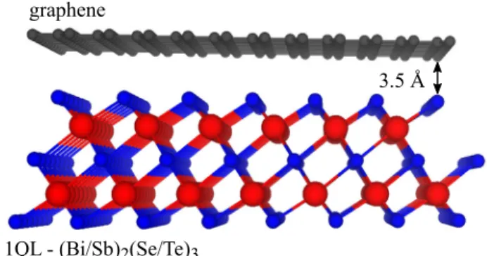
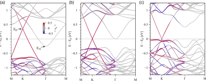
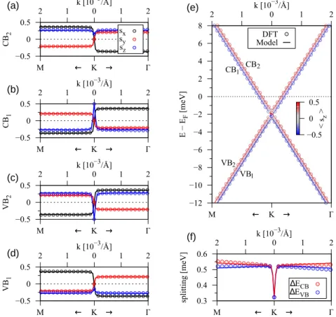
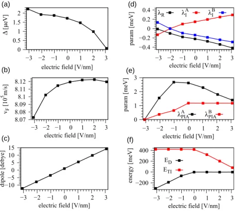
Heterostructures of Graphene and Topological Insulators Bi2
9
0
0
Volltext
(2)
(3)
(4)
(5)
(6)
(7)
(8)
(9)
Abbildung

+2
ÄHNLICHE DOKUMENTE
We show that superlattices based on zero-gap semiconductors such as graphene and mercury telluride exhibit characteristic Bloch–Zener oscillations that emerge from the
We investigated the relevance of IRAG and the cGKI stimulated phosphorylation of the calcium channel InsP 3 R-I for the NO/cGMP-dependent inhibition of pla- telet aggregation
from the principle of stationary energy, which is logically more satisfactory for many people, especially in view of the fact that maximum or minimum principles
The main international consequence of allowing oil exports (including for Russia) would be to slightly reduce the world price of oil (as a result of slightly higher U.S.
Elizabeth Rosenberg is a Senior Fellow and Director of the Energy, Environment and Security Program at the Center for a New American Security. Rosenberg served as a Senior Advisor
Crowdsourcing and Mobile Technology to Support Flood Disaster Risk Reduction.. Linda See, Ian McCallum, Wei Liu, Reinhard Mechler, Adriana Keating, Stefan Hochrainer- Stigler,
In particular, we obtain a reconstruc- tion of the potential function and its derivatives using only nodal data.. Results are a generalization of Law’s and
The inverse nodal problem was initiated by McLaughlin [1], who proved that the Sturm-Liouville problem is uniquely determined by any dense subset of the nodal points.. Some
