Opto-Electronic Effects in HgTe Based Nanostructures
DISSERTATION
zur Erlangung des Doktorgrades der Naturwissenschaften doctor rerum naturalium
(Dr. rer. nat.) Fakult¨at f¨ur Physik Universit¨at Regensburg
vorgelegt von
Dipl.-Phys. Christina Zoth
aus G¨ottingen
im Jahr 2014
Pr¨ufungsausschuss:
Vorsitzender: Prof. Dr. Gunnar S. Bali 1. Gutachter: Prof. Dr. Sergey D. Ganichev 2. Gutachter: Prof. Dr. Christian Sch¨uller weiterer Pr¨ufer: Prof. Dr. Thomas Niehaus
1 Introduction 5
2 Theoretical Basics 8
2.1 Band Structure of Mercury Telluride . . . 8
2.2 Photogalvanic Effects . . . 12
2.3 Photoconductivity Effect . . . 16
2.4 Cyclotron Resonance . . . 17
2.5 Quantum Transport Phenomena . . . 18
3 Experimental Methods 22 3.1 Experimental Setup . . . 22
3.2 Investigated Samples . . . 26
3.2.1 Mercury Telluride Quantum Well Samples . . . 26
3.2.2 Diluted Magnetic Semiconductor Samples . . . 30
3.3 Electrical and Optical Measurement Techniques . . . 32
3.3.1 Characterization via Magneto-Transport Measurements . 32 3.3.2 THz Radiation Induced Photocurrents . . . 34
3.3.3 Measurement of Photoresistance . . . 34
3.3.4 Measurement of Radiation Transmittance . . . 35
3.4 Development and Characterization of THz Waveplates . . . 36
4 Magnetogyrotropic Photogalvanic Effect in a Diluted Mag- netic Semiconductor Heterostructure 38 4.1 Experimental Results . . . 38
4.2 Discussion . . . 41
4.3 Brief Summary . . . 45
5 Dirac Fermion System at Cyclotron Resonance 46
5.1 Terahertz Induced Photogalvanic Effects . . . 46
5.1.1 Photocurrents at Zero Magnetic Field . . . 47
5.1.2 Cyclotron Resonance Assisted Photocurrents . . . 48
5.2 Photoresistance Measurements . . . 54
5.3 Discussion . . . 56
5.3.1 Photocurrents at Zero Magnetic Field . . . 56
5.3.2 Photocurrents and Photoresistance under Cyclotron Res- onance Condition . . . 57
5.3.3 Microscopic Picture of Current Generation . . . 62
5.4 Brief Summary . . . 65
6 Quantum Oscillations in Mercury Telluride Quantum Wells 68 6.1 Experimental Results . . . 68
6.1.1 Results for a Parabolic Dispersion . . . 69
6.1.2 Results for a Dirac Fermion System . . . 75
6.2 Discussion . . . 77
6.2.1 Microscopic Picture of Current Generation . . . 78
6.2.2 Analysis of the Photocurrents . . . 81
6.2.3 Analysis of the Photoresistance . . . 86
6.3 Brief Summary . . . 88
7 Conclusion 90
References 92
The spin of electrons and holes in solid state systems attracts growing atten- tion in modern research. This is stimulated by the hope that the spin degree of freedom in semiconductor systems can be utilized for new spin based elec- tronics, namely spintronics [1, 2]. The success of spintronics depends on the ability to create, manipulate and detect, as well as to transport and store spin orientations [3]. Possibilities of spin manipulation are e.g., the application of light or an electric field to a semiconductor heterostructure. A promising physical effect which can be exploited for this kind of spin manipulation is the spin orbit interaction [4, 5]. Therefore, semiconductors which are character- ized by a strong spin orbit interaction form a suitable system for spintronic applications [6].
A very promising candidate is mercury telluride, which has recently advanced into the focus of condensed matter research. In particular, the strong spin orbit interaction in mercury telluride is responsible for its unique energy spectrum yielding very fascinating effects [7–13]. Herein, without changing the material it is possible to obtain an inverted and normal parabolic band structure, as well as a linear one. The latter state is described by the Dirac theory of massless fermions [12]. In mercury telluride this Dirac-like dispersion can be realized in different manners: either by layered quantum well structures with a characteristic quantum well width or in topological insulator systems. The main difference lies in the spin degeneracy of the Dirac cone and the topology of the band structure in real space. In the former case the linear band structure is formed by unpolarized two dimensional Dirac fermions. This state is not bound to any spatial limitation [13–15]. In case of topological insulators the Dirac states only emerge at the edges or on the surface of a two or three dimensional mercury telluride system, respectively. Furthermore the states demonstrate a spin polarization [10]. This gives rise to the existence of dissipationless spin polarized transport along the one dimensional edge channels or the two dimensional surface states, as back scattering with spin flip is prohibited [10, 12, 16].
An interesting and powerful access to the study of spin related phenomena is provided by opto-electronic techniques. In particular, using radiation in the terahertz range the observation of effects of carrier redistribution in momen- tum space becomes possible e.g., photogalvanic effects [17]. Moreover, the measurements of opto-electronic effects build a bridge between the two fields of transport and optical phenomena [1]. The fundamental theory of these phe- nomena e.g., photogalvanic effects, photoconductivity or quantum transport are introduced in Chapter 2. Chapter 3 contains details about the experimen- tal setup and gives an overview of the investigated samples.
The observation and study of the terahertz radiation induced magnetogy- rotropic photogalvanic effect in various mercury telluride quantum well systems forms the core of this thesis. Herein several new phenomena are observed. In order to understand this opto-electronic and spin dependent effect, results for a well established semiconductor system will be presented in advance as this will substantially help to understand the observations for the mercury telluride structures. For this purpose quantum well structures based on cadmium tel- luride and indium arsenide with a diluted amount of magnetic manganese are investigated [18,19]. The results will be illustrated and discussed in Chapter 4.
In Chapters 5 and 6 the results of the opto-electronic measurements on mercury telluride based quantum well nanostructures are presented. In the scope of this thesis, the first investigations of cyclotron resonance assisted photocurrents and photoresistance on a Dirac fermion system are performed: the results which are presented and discussed in Chapter 5 for a mercury telluride sample with the critical quantum well width give experimental proof that the structure under investigation is indeed characterized by a Dirac-like energy spectrum [14, 15].
It is shown that nonlinear transport experiments can be utilized to probe the dispersion of two dimensional Dirac fermions.
Moreover, oscillations in the terahertz induced cyclotron resonance assisted photocurrent and photoresistance are observed for all types of band struc- ture, namely for normal and inverted parabolic, as well as linear [20]. These oscillations are induced by the variation of an external magnetic field. The corresponding experimental observations are presented in Chapter 6. It will be demonstrated that they originate from the crossing of the Fermi level with
Landau levels. This consecutive crossing results in the oscillations of spin polarization and electron mobilities in the spin subbands (cones), which are related to the de Haas-van Alphen and Shubnikov-de Haas effect.
Finally, Chapter 7 gives a conclusion of the main outcome of this work.
This thesis is devoted to mercury telluride (HgTe), in particular to effects concerning the special band structure of the material. Therefore, it is crucial to understand the main characteristics of the dispersion and its dependency on the width of the HgTe layer. These relations will be introduced in the first section of this chapter as a simplified model of band ordering. The HgTe samples are investigated by means of high frequency nonlinear opto-electronic phenomena, namely terahertz induced photogalvanic and photoconductivity effects. Hence, the following section will also depict the fundamental model of photocurrent generation in parabolic semiconductor quantum well structures which is based on an asymmetric spin dependent distribution of a charge carrier ensemble in momentum space. Additional effects induced by terahertz radiation are photoconductivity and cyclotron resonance, which will be introduced in the third and forth section of this chapter. For interpretation and analysis of the experimental results given in Chapters 5 and 6 quantum transport phenomena are needed. Therefore, the last section will illustrate the Shubnikov-de Haas and de Haas-van Alphen effect.
2.1 Band Structure of Mercury Telluride
HgTe belongs to the group of II-VI semiconductors and crystallizes in zinc- blende structure [21]. In quantum well (QW) structures, sandwiched between layers of cadmium telluride (CdTe), HgTe features an unique and very inter- esting dispersion, which can be influenced in an extraordinary way. While the conduction band of bulk CdTe is formed by s-states located at the group II atoms and the valence band by p-states at the group VI atoms, the situation for bulk HgTe is vice versa, yielding an inverted band ordering around the Γ point of the Brillouin zone [12, 22]. This effect of an inverted band structure is induced by the strong spin orbit interaction in this material [22, 23] and is depicted in Fig. 1. For bulk CdTe the Γ6 band is s-type and lays energeti- cally above the p-type Γ8 bands. These present conduction and valence band, respectively. In case of bulk HgTe the picture is quite different: the p-type Γ8 bands and the s-type Γ6 band are inverted compared to bulk CdTe. The
Figure 1: Energy spectrum of (a) bulk CdTe with a normal band ordering and band gap Egap, as well as of (b) bulk HgTe with an inverted band ordering and zero band gap between valence and conduction band, H1 and LH1, respectively. The band ordering for CdTe/HgTe QWs is depicted in (c) and (d): for QW widths LW smaller than the critical width LC the electronic structure is normal, whereas in case of LW > LC it is inverted.
Picture according to Ref. [11].
conduction and valence band consist of the light hole bandLH1 and the heavy hole bandH1 of the Γ8 bands and yield a zero gap system [18].
In HgTe based heterostructures this band ordering changes compared to the HgTe bulk material. Due to confinement effectsLH1 and H1 are separated by an energy gap and conduction and valence band are now formed of the heavy
hole H1 and the electron E1 band [22]. According to Ref. [11] only these two spin degenerated bands E1± and H1± are relevant, as they are close to the Fermi energy.
The corresponding effective Hamiltonian near the Γ point is given by Hef f(kx, ky) = H(k) 0
0 H∗(−k)
!
H =ǫ(k) +di(k)σi,
(1)
whereσi are the Pauli matrices and d1+id2 =A(kx+iky),
d3=M −B(kx2+k2y), ǫk=C−D(kx2+k2y).
(2)
Herekx and ky are momenta in the plane of the two dimensional electron gas and A, B, C and D are material specific constants. M is the Dirac mass pa- rameter, indicating the order of bands. In conventional semiconductors e.g., CdTe, this parameterM is positive (E1 lays overH1). However, for HgTe hav- ing an inverted band structure (H1 lays over E1) this parameter is negative.
Hence, in HgTe/CdTe QW structures the Dirac mass parameter M can be tuned from positive to negative values simply by varying the QW widthLW. At a special QW width LC the mass parameter M is zero and a topological quantum phase transition occurs, where the system merges from normal to in- verted band ordering. At this point the structure is characterized by the Dirac equation for massless particles [12]. This dependency ofE1 andH1 on the QW width LW is shown in Fig. 2 (a). Figure 1 (c) and (d) show the positions of the two bands (H1 and E1) in a CdTe/HgTe QW for LW smaller and larger than the critical widthLC. In the former case the band ordering of CdTe dom- inates, consequently the band structure is normal, whereas in the latter the bands have the ordering of HgTe, namely an inverted band structure. Note, that the band ordering can additionally be tuned by temperature and strain for bulk and two dimensional HgTe structures, as well as by the fractionx in Hg1−xCdxTe crystals, for review see Ref. [22, 24–26]. At the touching point of
the bands E1 and H1, indicated in Fig. 2 (a), the electronic structure of the system is formed by a mixture of the two bands and shows a linear dispersion.
This so-called Dirac cone is depicted in Fig. 2 (b), where the colors indicate the mixing of bands. A red shading stands for a dominant H1 state, whereas in blue regions the dominant state is E1. Purple shading is a mixture of both.
According to Refs. [11, 15] the Dirac cone is formed by the four states
|E1,+1/2i=f1(z)|Γ6,+1/2i+f4(z)|Γ8,+1/2i,
|H1,+3/2i=f3(z)|Γ8,+3/2i,
|E1,−1/2i=f1(z)|Γ6,−1/2i+f4(z)|Γ8,−1/2i,
|H1,−3/2i=f3(z)|Γ8,−3/2i,
(3)
wheref1(z),f3(z) and f4(z) are the envelope functions, z is the growth direc- tion, |Γ6,±1/2i, |Γ8,±1/2i and |Γ8,±3/2i are the basis functions of the Γ6 and Γ8 band. These are degenerated fork = 0, and are coupled by an effective
Figure 2: (a) Energy of the E1 and the H1 band depending on the QW width LW with the crossing point of bands atLW =LC. At this point the band structure is characterized by a linear behavior, where two dimensional massless Dirac fermions are predicted to occur. (b) shows the Dirac cone for the critical width LC. Colors indicate the mixing of bands: while red stands for a dominantH1 state, blue corresponds to theE1 state. Shades in between (purple) indicate a mixture of both. Picture according to Ref. [11].
Hamiltonian atk 6= 0. Consequently, the spin-up and -down bands are formed by a mixture of the different states of Eq. (3).
This Dirac-like dispersion can be achieved in different HgTe based systems.
The main subject of Chapter 5 is this linear band structure which has its ori- gin in the critical QW widthLC. Another possibility is provided by quantum phase transitions at the interface of HgTe to materials with normal band struc- ture. In case of a two dimensional system a Dirac-like dispersion arises at the edges, whereas for three dimensional systems it occurs at the surfaces of HgTe.
These systems with edge and surface states belong to the class of topological insulators, where dissipationless transport is possible by the mentioned states.
As topological insulators are not the subject of this thesis, their properties will not be illustrated in more detail. For review see Refs. [10, 12].
2.2 Photogalvanic Effects
Terahertz (THz) radiation induced effects are very useful and efficient for the investigation of semiconductor structures [17]. The photon energy in this spec- tral range is much smaller than the energy gap of conventional semiconduc- tors. Hence, no free carriers are generated across the band gap by absorption of photons. As a consequence, effects based on the redistribution of carriers in momentum space are observable. This redistribution results in adcelectric current without external bias [17]. An example are THz radiation induced photocurrents. Phenomenologically it is convenient to describe such dc cur- rents by writing the coordinate and time dependent electric current density j(r, t) = σE(r, t) as an expansion of powers of the electric field
E(r, t) =E(ω,q)e−iωt+iqr+E∗(ω,q)eiωt−iqr, (4) at radiation frequencyω and photon wavevector q as [27]:
jα(r, t) =h
σ(1)αβEβ(ω,q)e−iωt+iqr+c.c.i +h
σ(2αβγ′)Eβ(ω,q)Eγ(ω,q)e−2iωt+2iqr+c.c.i +σαβγ(2) Eβ(ω,q)Eγ∗(ω,q) +....
(5)
Herein, Greek indices are Cartesian coordinates and c.c. stands for the com- plex conjugate. Eq. (5) is limited to second order effects only. While the first term on the right-hand side describes the linear transport, the second and third term refer to second order electric field effects: the former term is responsible for second harmonic generation, the latter one for time indepen- dent contributions, which yield dc currents in response to the radiation’s ac electric field. The first two terms are out of scope of this thesis which deals with nonlinear transport phenomena proportional to the square of the electric field (∝ Eβ(ω,q)Eγ∗(ω,q)). The lowest order of non vanishing terms for the current density j relevant for the experimental observations of this thesis is given by [17]
jλ =X
µ,ν
χλµνEµEν∗, (6)
whereEν∗ =Eν∗(ω) = Eν(−ω) is the complex conjugate of Eν and χ is a third rank tensors. Equation (6) corresponds to the photogalvanic effect (PGE), whose sum on the right-hand side can be also written withEµEν∗ as a sum of symmetric and antisymmetric product
EµEν∗ ={EµEν∗}+ [EµEν∗], (7) yielding the photocurrent density to
jλ =X
µ,ν
χλµν{EµEν∗}+X
µ,ν
χλµν[EµEν∗]. (8) The photogalvanic effect is decomposed into the linear and circular photogal- vanic effect (LPGE and CPGE), given by the first and second sum on the right-hand side.
By applying an external magnetic field B, all the characteristic features of the LPGE and CPGE change and new phenomena arise e.g., the magnetogy- rotropic photogalvanic effect (MPGE). This effect will be introduced in the following, as it is the relevant mechanism of current generation for almost all findings presented in the experimental Chapters 4 to 6 of this thesis. It will be discussed briefly with the help of a simplified phenomenological description and then on the basis of a microscopic model.
Within the linear approximation of the magnetic field strengthB, the current density for the magnetic field induced photocurrent is given by [28, 29]
jα =X
β,γ,δ
φαβγδBβ{EγEδ∗}+X
β,γ
µαβγBβeˆγE2Pcirc. (9) Here, the fourth rank pseudotensorφis symmetric in the last two indices and µ is a third rank tensor. The first sum on the right-hand side is induced by linear components of radiation and even by unpolarized light, whereas the second sum requires circularly polarized radiation. This effect only occurs in gyrotropic media which are characterized by the lack of inversion symmetry and where nonzero components of third rank tensors exist [17, 30, 31]. Gyrotropic media have second rank pseudotensors as invariants. This means that the gyrotropic point group symmetry does not distinguish between polar vectors e.g., current or electron momentum and axial vectors e.g., magnetic field or spin [30]. This is the case for quantum well structures based on zinc-blende semiconductors e.g., HgTe QWs.
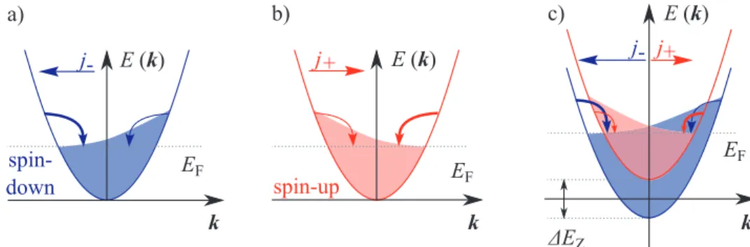
Besides this phenomenological description, the MPGE can also be explained by a microscopic model. Starting point is an electron gas homogeneously heated up by Drude absorption of THz radiation. In gyrotropic media the electron- phonon interaction contains an additional, asymmetric spin dependent term and is given by [5]
Vkk′ =V0+X
α,β
Vαβσα(kβ +k′β), (10) whereV0 describes the conventional spin independent scattering. V is a second rank pseudotensor, σα represents the Pauli matrices and k (k′) is the initial (scattered) wavevector. Note, that microscopically this additional term which is proportional to σα(kβ +kβ′) has the same origin as the structure and bulk inversion asymmetry [6, 32–34]. This asymmetry in the electron-phonon inter- action results in nonequal relaxation rates for positive and negative wavevectors within one energy subband. This is depicted in Fig. 3 (a) and (b) for the spin- down and -up subband. The difference in the arrows’ thickness corresponds to the probability Wkk′ ∝ |Vkk′|2 of electron-phonon scattering. This scatter- ing probability is unequal for positive and negativek within one subband and
leads to an asymmetric carrier distribution in k-space. Each subband yields an electron flux j±, where + and - stand for spin-up and -down. This effect is called zero bias spin separation [5]. The two electron fluxes are of equal strength but oppositely directed (j+ =−j−). Thus, the total electric current is zero, but a pure spin current js is created given by [5]
js= 1
2(j−−j+). (11)
By applying an external magnetic field B the two subbands split up energeti- cally due to the Zeeman effect. The difference in energy is given by [35]
∆EZ =gµBB, (12)
whereg is the effective Land´e factor of the material and µB is the Bohr mag- neton. As a result one of the subbands is now preferentially occupied. This results in an imbalance of the two electron fluxes and therefore, they do not cancel each other out anymore (see Fig. 3 (c)). This gives rise to a net electric
Figure 3: Asymmetric relaxation process of a homogeneously heated two dimensional electron gas for (a) spin-down and (b) spin-up subbands. This effect is called the zero bias spin separation. The difference in the arrows’
thickness corresponds to the scattering probability of electrons by phonons, which is unequal for positive and negative k within one subband. This yields an asymmetric carrier distribution and consequently an electron flux j± in each subband. By applying an external magnetic field the subbands split up energetically due to the Zeeman effect. This results in an imbalance between the electron fluxesj+ and j− and is depicted in (c).
currentjZwhich is proportional to the Zeeman splitting ∆EZ and consequently linear in B [29]:
jZ =−e∆EZ
EF
js= 4eSjs. (13)
Equation (13) is valid for a degenerated two dimensional electron gas and for a low degree of spin polarization, namely for ∆EZ/2<< EF, with Fermi energy EF [5, 28]. S is the magnitude of the average spin along the direction of B and is given by S = 2(nn++−+nn−
−), with carrier density n± in spin-up and -down subband. For a degenerated two dimensional system the average spin is given byS = −4E∆EZ
F [5].
Note, that there is a second microscopic mechanism contributing to the MPGE which is related to the spin dependent indirect optical excitation of carriers due to THz absorption in the presence of an external magnetic field. This effect can be explained analogue to the asymmetric relaxation process described above [5, 17].
2.3 Photoconductivity Effect
Besides THz radiation induced photocurrents, the radiation also results in a change of conductivity of the semiconductor. For radiation in the THz range and neglecting effects of impurity ionization, this phenomenon is limited to one band as the photon energy is too small for the generation of free carriers across the band gap. Hence, the carrier density n can be assumed to be constant and the photoconductivity ∆σ is solely given by the change of mobility ∆µ according to [17, 35]
∆σ =|e|n∆µ, (14)
with elementary charge e and with respect to the dark conductivity without radiation σ0 = |e|nµ0. µ0 is the mobility in the dark i.e., without THz radi- ation. The change of mobility ∆µ originates from the change of the carriers’
temperature due to electron gas heating by THz absorption. This absorption is drastically enhanced under cyclotron resonance conditions (see Section 2.4),
causing an intensified two dimensional electron gas heating. Therefore, mea- surements of the photoconductivity represent one of the established methods (next to radiation transmittance, see Section 3.3.4) of determining the effect of cyclotron resonance [14, 36].
2.4 Cyclotron Resonance
Free carriers moving in a two dimensional layer with an external magnetic field applied perpendicular to the QW plane experience a deflection due to the Lorentz force FL =q[v×B]. The carriers are bound to circular orbits in k-space normal to the magnetic field with an angular frequency given by
ωc = qB
m∗. (15)
Herein, m∗ is the effective electron (hole) mass and q is the charge, which is equal to -e for electrons and +e for holes [37]. High frequency radiation of exactly this angular frequencyωc results in a resonant absorption, namely the effect of cyclotron resonance (CR). The power absorbed by the free carriers for circularly polarized radiation is given by [35]
P±(ω)∝ 1
1 + (ω±ωc)2τ2, (16)
where the signs stand for right- (σ+) and left-handed (σ−) circular polarization and τ is the momentum relaxation time. For linearly polarized light, which is a superposition of σ+ and σ− polarization, the absorbed power adds up to [35, 37]
Plinear(ω)∝ 1
1 + (ω+ωc)2τ2 + 1
1 + (ω−ωc)2τ2. (17) A necessary requirement in order to observe CR is ωcτ ≫ 1. This condition guarantees that the free carriers can perform a whole orbit before being scat- tered by e.g., impurities. In quantum mechanics, for kBT < ~ωc, the effect of CR can be considered as a resonant transition between successive Landau levels (see Section 2.5) [35].
When the resonance condition is fulfilled (ω =ωc) andωcτ ≫1 two cases have to be distinguished: electrons and holes differ in their direction of rotation for
a fixed magnetic field polarity. Hence, electrons and holes only absorb one kind of circularly polarized radiation [38].
Considering holes and positive magnetic fields (q = +e > 0, B > 0, conse- quently ωc >0 according to Eq. (15)) the resonant absorption of light is only given forσ− polarization. The situation for electrons is vice versa. In the case of linearly polarized light, the effect of cyclotron resonance occurs for both carrier types and magnetic field polarities.
2.5 Quantum Transport Phenomena
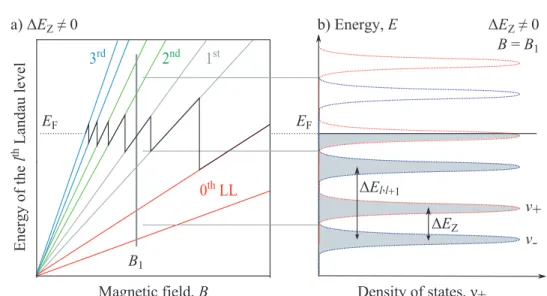
The application of high magnetic fields perpendicular to a two dimensional quantum well plane at low temperatures (kBT < ~ωc [39]) leads to a quanti- zation of the energy spectrum into discrete Landau levels. In that case each Landau level corresponds to a discreteδ peak in the density of states [39]. In a realistic system these levels are broadened due to finite temperatures and scattering. This is sketched in Fig. 4 (b).
The energy of the l-th Landau level for a parabolic energy spectrum is given by [6, 40]
El =~ωc(l+1
2) (18)
with l ∈N0, yielding a distance between two neighbored Landau levels l and l±1 of ∆El,l±1 = ~ωc. Taking into account Zeeman splitting according to Eq. (12) the number of carriers on each spin split Landau level is given by nLL =|e|B/h. For an electron gas with carrier density n the number of filled Zeeman split Landau levels (so-called filling factorυ) is given by [40]
υ = n nLL
= nh
|e|B, (19)
with Planck constant h. If n is fixed the Fermi energy EF oscillates as a function of the applied magnetic field [40,41]. These oscillations i.e., the jumps ofEF depend on the density of statesν± [39]. If there are e.g.,l Landau levels completely populated and the (l+ 1)-st is partly filled, thus the Fermi energy EF lies within the level l+ 1. If B increases the Landau level l+ 1 shifts up
Figure 4: Sketch of (a) spin splitted Landau levels and Fermi energyEF as a function of the magnetic fieldB for a parabolic dispersion and (b) density of sates ν± for a fixed B = B1 with Landau level and Zeeman splitting,
∆El,l+1 and ∆EZ.
in energy and is emptied. Thus, EF falls back onto the level below [39]. This is sketched for an ideal system with δ function Landau levels in Fig. 4 (a).
Herein, every jump of the Fermi energy corresponds to a filling factorυ: even filling factors correspond to jumps between two Landau levels of different l, whereas odd filling factors stand for jumps within a Zeeman split Landau level.
By variation of the magnetic field strength B, the Landau levels and corre- sponding peaks in the density of states are pushed through the Fermi energy.
This consecutive crossing ofEl andEF can also be induced by keepingB fixed and varying EF. Either results in an oscillating behavior of many physical parameters which are periodic in 1/B. In this work oscillations of the mo- bility of free carriers and their magnetic momenta are of interest, namely the Shubnikov-de Haas and the de Haas-van Alphen effect.
Shubnikov-de Haas Effect Figure 4 (b) indicates that the density of states at EF varies with the magnetic field B. If EF lies in between two Landau levels, the density of states at EF is zero, whereas it has a maximum when EF is in the middle of a broadened Landau level. This can be directly seen in a
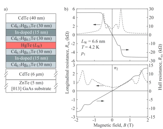
system’s longitudinal resistanceRxx(B) which is illustrated in Fig. 5 (a) for a 8 nm HgCdTe QW Hall bar structure at 4.2 K. The resistance has a minimum when EF lies between two Landau levels (zero density of states) and is finite when it lies within a Landau level [39]. This oscillating behavior of Rxx as a function ofB is the Shubnikov-de Haas (SdH) effect. Furthermore, Fig. 5 (a) demonstrates that for low magnetic fields Rxx(B) is constant. This is due to the fact that when B goes to 0, the Landau levels decrease their distance in such a way that they eventually overlap. In this case EF always lies within this constant density of states and the resistance becomes constant [40].
Each minimum of Rxx(B) can be related to a filling factor υ (indicated in the figure) which plotted against 1/B yields a straight line with a slope of hn/e. This is shown in the inset of Fig. 5 (a). Hence, the Shubnikov-de Haas oscillations are periodic in 1/B. The analysis of the oscillations can provide information about the carrier density, occupation of higher subbands, which can be seen by two different frequencies in the SdH oscillations, or the evolution of Zeeman spin splitting [39]. The latter can be seen in Fig. 5 (a): for magnetic fields larger than ≈ 2.76 T (value corresponds to tiny dip between filling factors 10 and 12) even and odd filling factors are observed.
This indicates the resolution of the Zeeman splitting of Landau levels.
De Haas-van Alphen Effect Another effect similar to the Shubnikov-de Haas effect originates from a periodic change of the total energy of the free carriers with the magnetic field, namely the de Haas-van Alphen effect. This can be detected experimentally as oscillations of the material’s magnetic momentum µm =−∂E/∂B [41]. For matters of simplification the spin is neglected in the following. The variation of the total energy of free carriers is depicted in Fig. 5 (b).
For B = 0 T the density of states is continuous (regions I and IV). When a magnetic field is applied the carriers squeeze onto discrete Landau levels. For the magnetic field B1 depicted in region II the system has the same energy as for zero magnetic field (region I): the number of carriers which raise their energy is equal to the number of carriers which degrade their energy in order to divide onto the Landau levels. When B is increased to a value of B2, the
total energy of the system increases as the highest carriers shift energetically up (region III). ForB3 the system’s total energy is back to the initial one (as in I, II or IV) as the uppermost carriers have to decrease in energy (region V) [41].
Consequently, the total energy has a minimum at points such as B1, B3, ...
and maximum points atB2, .... This oscillation in energy with a periodicity of 1/B can be seen in the free carriers’ magnetic momentum and hence, in their spin S, as µm ∝S.
Figure 5: (a) Measurement of Shubnikov-de Haas oscillations in the longi- tudinal resistanceRxxof a 8 nm HgCdTe Hall bar sample. Numbers indicate filling factors υ. The inset shows the filling factor υas a function of the in- verse magnetic field 1/B. The de Haas-van Alphen effect is depicted in (b) as a simplified model of the free carriers’ total energy; the Zeeman effect is neglected. Whereas the density of states is continuous for B= 0 T (regions I and IV), it splits into Landau levels when a magnetic field is applied. In the case of B1 (II) andB3 (V) the total energy is the same as forB = 0 T as the same amount of carrier decrease their energy, as increase it. For B2 the total energy is increased as the uppermost carriers shift energetically up (III).
This chapter is devoted to the experimental methods used for the investigations in this work. In order to give a clear picture of the performed measurements the whole experimental setup is depicted first. Then the studied samples are introduced, which can be divided into two groups: diluted magnetic semicon- ductor (DMS) QW structures and - forming the core of this thesis - HgTe based QW structures. In the third section of this chapter the different measurement techniques are illustrated. These comprise mere electrical and optical, as well as opto-electronic measurement techniques. As the variation of polarization of the THz radiation plays an important role for some of the studied effects e.g., cyclotron resonance, two types of waveplates will be presented.
3.1 Experimental Setup
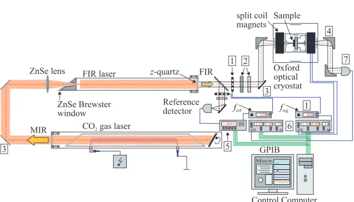
The experimental setup used for the measurements includes a laser system, an optical cryostat with a superconducting split coil magnet, as well as optical chopper systems and other devices. They are all combined in a complex struc- ture, which will be introduced in the following. The whole experimental setup can be seen in Fig. 6.
The laser system consists of an electrically pumped continuous wave (cw)PL51 CO2 gas laser, emitting in the mid-infrared (MIR) range, and a 295FIR1 gas laser. This is optically excited by the CO2 gas laser and emits in the far- infrared range (FIR). The THz radiation of the FIR laser is line tunable and its wavelength depends on the kind of gas filled into the cavity, as well as on the exact wavelength of the exciting MIR radiation. For this thesis a wavelength of 118.8µm was used. The parameters of the operating laser system are given in Tab. 1.
The CO2 gas laser belongs to the group of vibrational and rotational gas lasers and is one of the most important representatives of the group of molecular lasers. It is longitudinal electrically excited and delivers a power of approxi- mately 35 W. The emitted wavelength can be tuned around and between the
1Edinburgh Instruments, Livingston, UK
Figure 6: Experimental setup with MIR (CO2) and FIR gas laser system.
The optical path is sketched as a red line. Most devices are labeled in the picture. 1: optical chopper, 2: waveplates or other optical devices, 3: planar mirror, 4: parabolic mirror, 5: digital multimeter, 6: lock-in amplifier, 7:
Golay cell. A detailed description is given in the text. Picture modified after Ref. [42].
lines of 9.4 and 10.4 µm. These lines belong to two different optical active transitions between vibrational modes of the CO2 molecule. The line tun- ing is possible as these vibrational modes split up into different rotational modes [17, 43]. The output radiation is not used for experiments, but acts only as an optical pump source for the second molecular gas laser. Hence, the radiation is deflected by two planar mirrors and focused by a zinc selenide (ZnSe) lens through a polarizing ZnSe Brewster window mounted on top of a steel cone into the cavity of the FIR laser system. The Brewster window ensures linearly polarized light, with the E-field vector being aligned horizon- tally. The incoming MIR radiation excites a vibrational state of the molecule of the second gas laser system having a permanent electric dipole moment.
λMIR laser (µm) FIR laser gas λ(µm) f (THz) E~ω (meV) P (mW)
9.695 methanol 118.8 2.53 10.35 60
Table 1: Parameters of the operating laser system: excitation wavelength λ of the CO2 gas laser; laser gas of the FIR laser system; wavelength λ, frequencyf, photon energyE~ω and powerP of the emitted THz radiation.
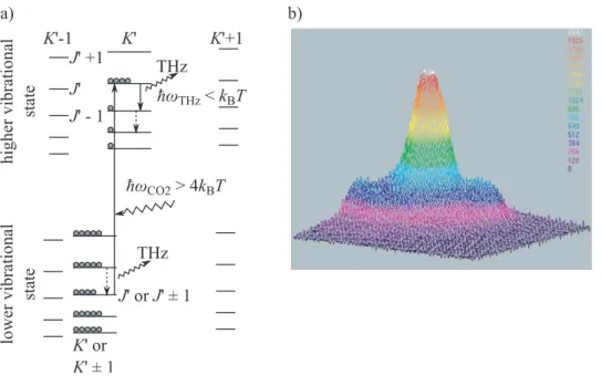
This is sketched in Fig. 7 (a) for a symmetrical top molecule, where K is the projection of the angular momentumJ on the symmetry axis of the molecule.
Assuming that the vibrational relaxation is slow enough, lasing transitions oc- cur between rotational states only emitting radiation in the FIR range [17].
The cavity of the FIR laser is closed by a silver coatedz-quartz window, which is transparent for wavelengths with frequencies in the THz range, but reflects the MIR radiation and so ensures a monochromatic output. The transversal mode shape can be adjusted by variation of the resonator length via screws at the silver coated quartz window. It can be monitored by thermal paper or by a P yrocam III2 in order to verify that the beam has a Gaussian shape (see Fig. 7 (b)). The emitted monochromatic FIR radiation of the molecular gas laser is directed through a beam splitter, consisting of Mylar3. The reflected part of the beam (≈ 15%) is used as a reference signal in the analysis of the measurements and allows to monitor the stability of the laser. It is modu- lated by a 300CD4 optical chopper with a frequency of fref = 140 Hz and directed to a pyroelectric reference detector LIE-329-Y5 by a planar mirror.
This reference signal Uref is measured by a KI20006 digital multimeter and sent to a control computer running a LabVIEW7 program. This LabVIEW program controls the whole experimental setup and records all measured data.
It was written by Wolfgang Weber8 and Sergey Danilov8. The main part of the beam (≈85%) is transmitted through the beam splitter and is modulated by a second 300CD4 optical chopper at a frequency of fsig = 620 Hz. At this
2pyrometer for temperature detection, Spiricon Inc., Logan, UT, USA
3a polyester film made from stretched polyethylene terephthalate
4Scitec Instruments, Wiltshire, UK
5Laser Components, Olching, Germany
6Keithley Instruments, Germering, Germany
7Laboratory Virtual Instrumentation Engineering Workbench
8Terahertz Center, Regensburg, Germany
point additional devices e.g., waveplates or analyzers can be inserted into the optical path. The integration of a step motor, which is operated by LabVIEW and rotates the mounted waveplates step wise, is possible. The beam is then deflected by a planar mirror and is focused by a parabolic9 one into a Spec- tromag SM4000-810 optical cryostat. The inner windows of this cryostat are made of z-cut quartz, the outer windows are fabricated of TPX11. As these are transparent for THz and visible light, the latter are covered with a black polyethylene sheet to prevent illumination of the sample with ambient light.
The sample is located in the middle of the cryostat between two supercon- ducting split coil magnets, allowing magnetic fields up to 7 T perpendicular to the sample’s surface. The magnetic field can by controlled by anIPS120-1010
9focal length f = 22.5 cm, Kugler GmbH, Salem, Germany
10Oxford Instruments, Abingdon, UK
11polymethylpenten
Figure 7: (a) Scheme of optically pumped THz transitions in a symmetric top molecule. Electrons are excited to a higher vibrational mode by the incoming CO2 gas laser radiation, yielding a population inversion in both states. Relaxation transitions occur between the rotational modes of both vibrational states, emitting radiation in the THz range. (b) Spatial beam shape with an average power of≈60 mW, recorded with the Pyrocam III2.
power supply. The temperature at sample position can be varied from liquid helium temperature (T = 4.2 K) up to room temperature, is maintained and measured by aLS33212 temperature controller. A wiring system connects the sample with twoSR830 DSP13 lock-in amplifiers, with an input resistance of 10 MΩ, allowing the measurement of two different voltage drops across the sample (compare Section 3.2 and 3.3). A part of the radiation is transmitted through the sample and leaves the cryostat on the other side. It is then par- allelized and focused, both by a parabolic mirror14, to a Golay cell detector15, whose output can be recorded via lock-in technique. The lock-ins are con- nected to the control computer via GPIB16 as well as the reference detector by a digital multimeter, temperature and magnetic field controller and step motor unit. As mentioned before, all variables are recorded and can be set by the LabVIEW program.
3.2 Investigated Samples
In the framework of this thesis two different groups of semiconductor struc- tures were investigated: HgTe based quantum well heterostructures of similar layer design, but different QW widthsLW and two diluted magnetic semicon- ductor QW structures. Their designs and properties will be introduced in the following.
3.2.1 Mercury Telluride Quantum Well Samples
The main part of this thesis is devoted to photocurrents in HgTe based QW structures. The samples were provided by Nikolai N. Mikhailov17 and Sergey A. Dvoretsky17. They were grown by molecular beam epitaxy (MBE) onto a (013) oriented gallium arsenide (GaAs) substrate [44]. These (013) grown QWs belong to the C1 point group possessing no symmetry restriction. The HgTe
12Lake Shore Cryotronics, Westerville, OH, USA
13Stanford Research Systems, Sunnyvale, CA, USA
14focal length f = 22.5 cm, Kugler GmbH, Salem, Germany
15Artas GmbH, Zeitlarn, Germany
16General Purpose Interface Bus
17Institute of Semiconductor Physics, Novosibirsk, Russia
Figure 8: (a) shows a cross section of the layer design of the investigated HgTe based QW samples. The QW layer with widthLW is indicated in red.
(b) depicts a typical result of a magneto-transport measurement by which all samples were characterized. The results of a 6.6 nm wide HgTe QW are presented for two different carrier types and densities p1 and n2 (see Chap- ter 5). The upper panel corresponds to ap-type sample, while the lower one shows an-type behavior. Solid lines show the Hall resistanceRxy with Hall plateaus, dashed lines are the longitudinal resistanceRxxwith Shubnikov-de Haas oscillations. They scale on the right and left, respectively.
QW is sandwiched between two layers of Cd0.7Hg0.3Te. Figure 8 (a) shows an exemplary cross section. Depending on the QW widthLW the band structure can change its ordering, as described in Section 2.1. This makes it possible to divide the samples into three groups of band structure: normal and inverted parabolic as well as linear.
The samples were prepared in different designs e.g., large area square shaped samples and Hall bars (see Fig. 9). These various designs are due to the differ- ent kind of measurements performed on the samples. While Hall bar structures
width LW (nm) design gating band structure
5 square no normal
6.4 Hall bar no linear
6.6 Hall bar yes & no linear
6.6 square no linear
8 Hall bar∗ no normal
8 square no inverted
21 square no inverted
Table 2: QW widthLW, design, gating and band structure of the investi- gated HgTe QW samples. ∗The QW contains cadmium: Hg0.86Cd0.14Te.
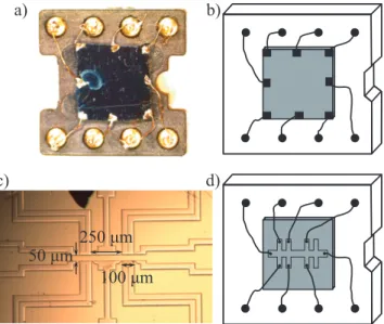
show best resolved Shubnikov-De Haas oscillations and quantum Hall plateaus, they are not ideal for photocurrent or transmission measurements. For this purpose the samples have to be large enough to ensure no illumination of the contacts or samples’ edges. Both can both give rise to other signals superim- posing the investigated effects. Therefore, radiation transmittance, as well as photocurrent experiments are mainly studied on large area 5×5 mm2 square samples, where the indium (In) contacting was done at the samples’ edges and corners only (see next section).
An overview of the studied HgTe QW samples, their design and band struc- ture is given in Tab. 2. All the samples have been characterized by magneto- transport measurements, as described in Section 3.3.1. Carrier densities are given in Chapters 5-6, where the experimental results are presented.
Normal Parabolic Band Structure Two samples with normal band structure were investigated. The first one is a pure HgTe QW with a widthLW = 5 nm, which is smaller than the critical width LC. Hence, it is characterized by a normal parabolic band ordering where the E1 band lies above the H1 band as known from conventional semiconductors (e.g., GaAs, CdTe or InAs). The sample’s design is a large area square with an edge length of 5 mm. Eight ohmic In contacts are soldered to the corners and to the middle of the edges (compare Fig. 9 (a) and (b)). These ohmic contacts are connected to the pins
of an eight-pin chip carrier via gold wires, which allow the measurement of the voltage drops induced by bias or THz radiation.
The second sample is a 8 nm HgCdTe QW Hall bar structure. It has a 14% Cd content in the QW, in contrast to all other pure HgTe QWs. As a consequence, the transition from normal to inverted parabolic band structure is obtained for wider QWs than for pure HgTe QWs [26, 45]. In case of the here investigated Hg0.86Cd0.14Te sample with a width of LW = 8 nm the dispersion is normal parabolic. The Hall bar structure is depicted in Fig. 9 (c) and (d). It is 50µm wide, with distances between the contacts of 100 and 250 µm. The contact pads of the Hall bar are soldered in the same way as the contacts of the square sample i.e., via In contacts and gold wires. The sample is mounted on an eight-pin chip carrier.
Linear Band Structure Increasing the QW width LW the E1 and H1 bands touch each other at a critical width LC of approximately 6-7 nm (see Fig. 2 (a)) [11,13,46]. At this point the dispersion shows a linear, Dirac-like behavior.
For this thesis a quantum well width of 6.6 nm was selected. Samples in both shapes, Hall bar and square, were investigated. Two Hall bar structures were available, prepared with and without gate. A gate enables a controllable way of carrier density variation. Therefore, an isolating layer of 100 nm silicon dioxide (SiO2) and 200 µm silicon nitride (Si3N4) is used with a metallic gate layer of titanium gold (TiAu) deposited on top. The gate layer can be biased via a pin of the eight-pin chip carrier to which it is connected by a gold wire.
Inverted Parabolic Band Structure As a last group samples with a QW width LW larger than the critical width LC were under study. For this case the elec- tron bandE1and heavy hole bandH1are exchanged in contrast to conventional semiconductors e.g., CdTe. Hence, they are characterized by an inverted band ordering. Two samples were available, with widths of 8 and 21 nm. The sam- ples’ design is a 5×5 mm2 square shape. The contacting is done in the same way as described above.
Figure 9: (a) shows a picture of a square shaped sample mounted on a chip carrier. It is connected to the pins via gold wires and In soldering.
(b) gives a schematic drawing of (a). (c) depicts a Hall bar structure with a width of 50 µm and distances between contacts of 100 and 250 µm. (d) shows the wiring of the Hall bar sample on a chip carrier.
3.2.2 Diluted Magnetic Semiconductor Samples
In DMS structures paramagnetic ions e.g., manganese (Mn2+), are introduced into the host material. These Mn2+ ions provide magnetic moments, which give the opportunity of a controllable variation of the magnetic properties of the semiconductor. This can be done by e.g., using different host materials, changing the Mn2+ concentration or varying the temperature. In the following, two DMS samples are investigated with different host materials: a CdTe based and an indium arsenide (InAs) based QW structure. Both samples are (001) MBE grown QW structures on a GaAs substrate. They are fabricated as large area squares of the same dimensions and contact preparation as the HgTe samples (see Section 3.2.1). Their properties are summarized in Tab. 3 of Section 4.1. (001) grown CdTe and InAs QW structures belong to the C2v
symmetry group. Both have two mirror planes perpendicular to the QW and a C2axis parallel to the growth direction. Depending on the host material (CdTe, II-VI or InAs, III-V) the Mn2+ ions result in different electrical properties.
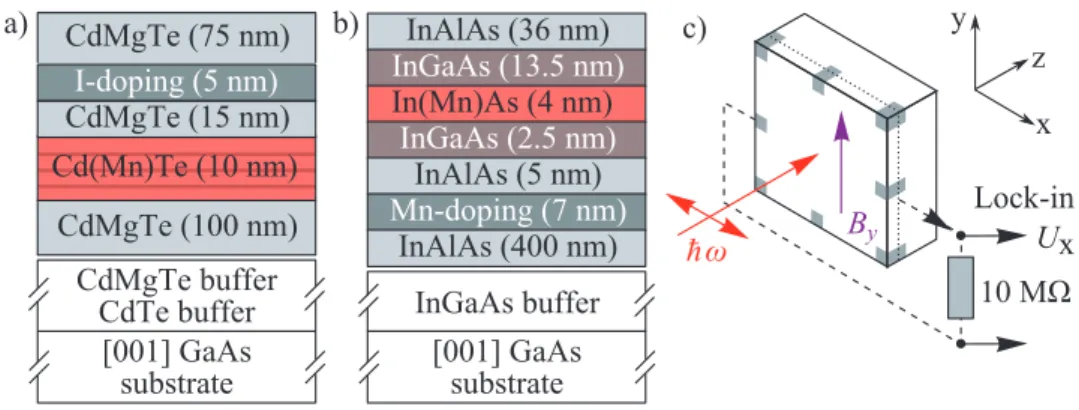
Among the DMS materials Cd(Mn)Te is one of the most intensely studied semi- conductor heterostructures. The sample was provided by the group of Tomasz Wojtowicz18. The 10 nm wide Cd(Mn)Te QW is embedded between two layers of Cd0.7Mg0.3Te (see Fig. 10 (a)). During the growth process three monolay- ers of Cd0.86Mn0.14Te were inserted applying digital alloy technique [47–49].
CdTe belongs to the group of II-VI semiconductors. In this case the Mn2+ is electrically neutral as it substitutes Cd2+, which has the same valence. But it provides a localized spin of 5/2 [18]. The sample is iodine (I) doped and characterized by an-conductivity.
The second DMS sample has an InAs host material. InAs is, in contrast to CdTe, a narrow band gap material just like HgTe. The structure is MBE grown by Dieter Schuh19 and Ursula Wurstbauer19 and has a 4 nm wide In(Mn)As QW embedded in a 20 nm In0.75Ga0.25As channel. Fig. 10 (b) depicts a cross section of the structure with a Mn2+ doping layer grown before the QW. Due to segregation processes the QW features a limited Mn2+ concentration [50–
52]. InAs belongs to the III-V semiconductor group. Therefore, the Mn2+
18Institute of Physics, Warsaw, Poland
19Terahertz Center, Regensburg, Germany
Figure 10: (a) depicts a schematic cross section of the Cd(Mn)Te sample.
Herein, three monolayers of Cd0.86Mn0.14Te were inserted during the growth of the 10 nm wide QW. (b) shows the In(Mn)As structure which has a Mn2+
doping layer inserted before the QW. Due to segregation of the manganese during the growth process, the 4 nm wide QW has a limited concentration of Mn2+. In (c) the experimental geometry is sketched, with inplane magnetic field and normal incidence of radiation.
ions provide free holes in addition to the localized magnetic moments as they substitute In3+. This results in a p-type conductivity of the In(Mn)As DMS sample [50, 53].
3.3 Electrical and Optical Measurement Techniques
At this point the different measurement techniques, which were used in this work, will be introduced. These comprise magneto-transport measurements, analysis of THz radiation induced photocurrents and photoconductivity (pho- toresistance), as well as the detection of the transmitted radiation through the sample.
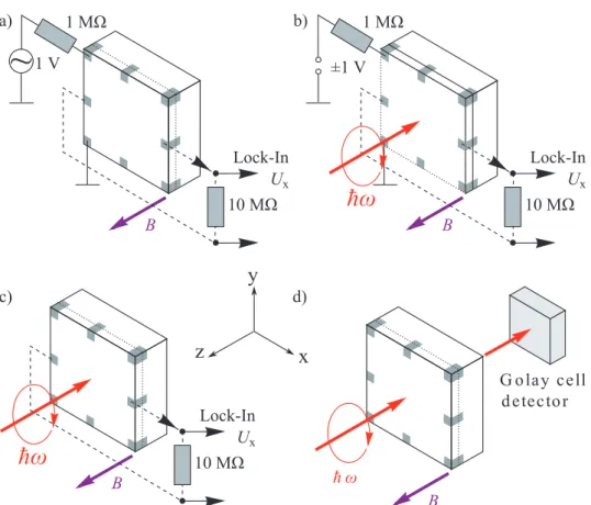
3.3.1 Characterization via Magneto-Transport Measurements Standard magneto-transport measurements were performed for every sample in order to determine carrier type and density. For this kind of measurement the sample wasacbiased with 1 V. The current was limited by a 1 MΩ resistor giving an ac current of 1 µA through the sample. An external magnetic field was applied normal to the QW plane. The signals Ux and Uy were measured with lock-in technique via a voltage drop over a 10 MΩ load resistor (compare Fig. 11 (a)). These signals correspond to the Hall and longitudinal resistance, respectively, using R = U/Iac. In most cases a Van-der-Pauw geometry was used. An exemplary result of such a measurement, which was performed on a 6.6 nm HgTe QW sample (see Chap. 5), is depicted in Fig. 8 (b) for two different carrier types and densities. Well pronounced Shubnikov-de Haas os- cillations and quantum Hall plateaus can be seen in the longitudinal (Rxx) and Hall (Rxy) resistance. The different slopes of the Hall resistance indicate the different carrier types: holes in the upper panel and electrons in the lower one.
To achieve a controllable variation of the carrier density some samples were prepared with a gate (compare Section 3.2) or the effect of persistent photo- conductivity was used [14, 54]: by illuminating the sample with a red light emitting diode (λ = 630 nm) for a defined time ti the carrier density can be changed. This process can be undone by heating the samples up to ≈ 150 K.
In the following this procedure is referred to as optical doping [54, 55].
Figure 11: Overview of the different measurement setups with a magnetic field B applied normal to the sample’s surface for (a) magneto-transport, (b) photoconductivity (photoresistance), (c) photocurrent and (d) radiation transmission. In (a) anaccurrent is sent through the sample and two voltage drops Ux and Uy (the latter is not shown) are measured. These signals are proportional to the Hall and longitudinal resistance. The setup for (b) is similar but with a dccurrent and THz radiation of normal incidence. For (c) the sample is unbiased but also with THz radiation. For (a)-(c) the signals Ui, withi=x, y, are measured as a voltage drop over a 10 MΩ load resistor via lock-in technique. Note, that the y direction can be measured analog to thexdirection which is indicated in the figure. (d) presents a pure optical measurement, where the transmitted radiation through the sample is detected by a Golay cell detector.
3.3.2 THz Radiation Induced Photocurrents
For the measurement of photocurrents the unbiased sample was illuminated under normal incidence with THz radiation. An external magnetic field was applied perpendicular to the sample’s surface. This radiation induces photo- currents, which were measured analog to Section 3.3.1, via a voltage drop over a 10 MΩ load resistor applying lock-in technique. The corresponding setup is depicted in Fig. 11 (c). In order to eliminate fluctuations of the laser power during a measurement the signalsUx and Uy were normalized by the recorded reference signal Uref. Then they were multiplied with the power calibration factor Pcalib given in units of (V/W) according to (Ui×Pcalib)/Uref in (V/W) withi=x, y. The calibration factor was obtained with aVector H41020 pow- ermeter by measuring the averaged laser output power P and normalizing it to a mean value of reference signalUref.
Note, that for the DMS samples, with C2v symmetry, photocurrents are for- bidden for normal incidence of light and a perpendicular magnetic field [24].
Therefore, the study of THz radiation induced photocurrents was done with an inplane magnetic field. This is shown in Fig. 10 (c).
3.3.3 Measurement of Photoresistance
As a complementary measurement studies of the photoresistance (or photocon- ductivity) ∆R were performed. ∆R corresponds to the change of the sample’s resistance when illuminating the structure with THz radiation. In order to dis- tinguish between the two THz radiation induced effects of photocurrent and photoresistance, the sample was biased individually either with a positive or a negativedc electric current of|Idc| = 1µA (±1 V, 1 MΩ). The magnetic field B and the propagation direction of the THz radiation were aligned normal to the sample’s surface. The voltage drops Ui,±, with i= x, y, for both currents
±Idc were recorded as sketched in Fig. 11 (b). While the effect of photoresis- tance (photoconductivity,Ui,P C±) is dependent on the current direction through
20Scientech Inc., Boulder, CO, USA
the sample, the photogalvanic effect (Ui,P GE± ) is not effected. Consequently, the difference of these two signals divided by the current, given by
∆Ri = Ui,+−Ui,−
2Idc
= (Ui,+P C +Ui,+P GE)−(−Ui,P C− +Ui,P GE− ) 2Idc
, (20)
corresponds to the change of resistance. It is inverse proportional to the change of conductivity and to the difference in mobility µ (see Section 2.3). These measurements are performed in addition to opto-electronic photocurrent mea- surements - the main topic of this work - and provide access to additional information e.g., on cyclotron resonance [36].
3.3.4 Measurement of Radiation Transmittance
For a further understanding measurements of radiation transmission were per- formed, which is a standard method for the identification of the effect of cy- clotron resonance. The corresponding setup is shown in Fig. 11 (d) with the magnetic field and the propagation direction of the THz radiation aligned nor- mal to the QW plane. Radiation transmittance is a sheer optical measurement technique; the sample was therefor without bias and no wiring was needed. A Golay cell21behind the sample detected the transmitted part of light and gave the signal to a lock-in amplifier. As the Golay cell is a very slow detector the modulation frequencyfsig of the radiation was reduced toftm≈30 Hz. Due to high thermal noise on the one hand and a slight hysteresis effect of the detec- tor on the magnetic field on the other hand, every transmission measurement was recorded twice (for both magnetic field sweeping directions) and averaged afterwards.
21Artas GmbH, Zeitlarn, Germany
3.4 Development and Characterization of THz Wave- plates
As the variation of the polarization state of radiation is important for many aspects of this work, in particular for the cyclotron resonance assisted mea- surements, it was necessary to use waveplates suitable for the THz range and of best possible quality.
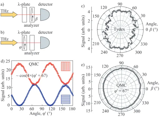
In cooperation withT ydex22 a special waveplate was developed applicable for a wide spectral region in the THz range, which is called achromatic waveplate.
The analysis of the conversion of linearly to circularly polarized light was done by rotating an analyzer mounted in a stepmotor unit behind the waveplate and measuring the transmitted radiation intensity with aLIE-329-Y23pyroelectric detector. Setup and results can be seen in Fig. 12 (a) and (c) for a wavelength ofλ= 118.8µm. The transmitted radiation intensity is almost independent of the angleβ of the analyzer. This means that theT ydexachromatic waveplate demonstrates a high quality of polarization conversion to circularly polarized light. Similar results were obtained for other wavelengths with frequencies in the THz range. Details can be seen in Ref. [56].
In addition a waveplate made for a wavelength of λ = 118.8 µm from QMC Instruments24 was verified. It features a special anti-reflection coating which increases the transmittance behavior of thez-cut quartz plates. As the plates had no indication of the optical axis it had to be determined experimentally.
For this purpose the linearly polarized radiation passes through the waveplate and then through an analyzer, aligned parallel or perpendicular to the initial linear polarization. The transmitted radiation is then detected with aLIE-329- Y22 pyroelectric detector as a function of the angle ϕ′. The angle ϕ′ of the waveplate is varied in 2◦ steps from 0 to 360◦ perpendicular to the propagating direction of the radiation. This setup can be seen in Fig. 12 (b). The signal of the transmitted radiation is measured for both grid alignments. This is shown in Fig. 12 (d). The two touching points at ϕ′ ≈ 67 and 157◦ correspond to circularly polarized radiation. For this case the horizontal and vertical linearly
22St.Petersburg, Russia
23Laser Components, Olching, Germany
24West Sussex, UK
polarized part of light have the same intensity. In order to analyze the quality of the waveplate the same measurement as for the achromatic waveplate was done (see Fig. 12 (a)). The result is shown in Fig. 12 (e). With a deviation from the mean signal of only 7% the waveplate demonstrates an excellent quality.
Many measurements of this thesis were carried out with right- or left-handed circularly polarized radiation. In these cases the waveplate fromQMC Instru- ments was used.
Figure 12: (a) and (b) show the setup for the analysis of the waveplates’
quality and estimation of the optical axis. (c) depicts the transmitted laser intensity in dependency of the analyzer rotation angle β for the achromatic waveplate fromT ydex for a wavelength ofλ= 118.8 µm. In (d) the trans- mitted radiation is detected depending on the rotation angleϕ′ of theQMC Instruments waveplate for two different grid positions of the analyzer and λ = 118.8 µm. (e) shows the same as (c) but for the QMC Instruments waveplate. The alignment of the waveplate is chosen as ϕ′ = 67◦ which corresponds to the first touching point in (d), where the transmitted part of radiation is fully circularly polarized.
a Diluted Magnetic Semiconductor Hetero- structure
The magnetogyrotropic photogalvanic effect is a rather novel opto-electronic method for the investigation of semiconductor heterostructures. In order to understand its spin dependent origin a well established semiconductor system will be analyzed before turning to the core of this thesis - the study of THz radiation induced photocurrents in HgTe based QW systems. A suitable can- didate for this are diluted magnetic semiconductor heterostructures as they are well characterized and provide an opportunity to control the sample’s magnetic properties. In this chapter the experimental observations for a Cd(Mn)Te and In(Mn)As DMS sample will be presented and discussed by means of the MPGE (compare Section 2.2). The results are published in Ref. [19]. Only a part of the experimental results of Ref. [19] are presented here.
4.1 Experimental Results
The THz radiation induced photocurrents in the unbiased DMS samples were measured as a function of a magnetic field By applied in the QW plane for different fixed temperatures. In addition, measurements of the temperature dependency of the photocurrents for a given magnetic field value were per- formed. As the measured directions x and y show a similar behavior, only the photocurrent jx normalized by the laser power P will be discussed here.
Furthermore, the observed currents have been shown to be an odd function of the magnetic field. Therefore, the presented curves are limited to positive By only. For excitation linearly polarized light was applied normal to the QW plane with a wavelength of 118.8µm.
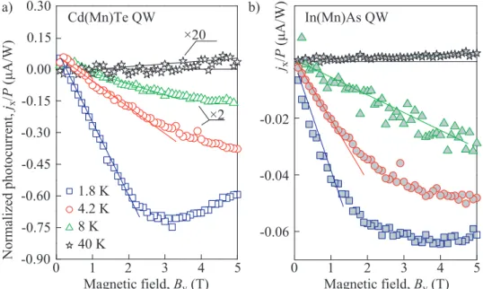
Figure 13 (a) shows the THz radiation induced currentsjx/P measured in the Cd(Mn)Te sample for temperatures of 1.8, 4.2, 8 and 40 K as a function of the inplane magnetic field. Note, that some curves are multiplied by a factor for a better comparison, indicated near the corresponding curve. For high tempera- tures or for low temperatures and small magnetic fields, the magnitude of the
photocurrent shows a linear behavior (solid lines in Fig. 13 (a)). Whereas, for lowT and highBy the current saturates with increasing magnetic field and for T = 1.8 K even shows a decrease for magnetic fields larger than ≈ 3 T. The maximum current of -0.74 µA/W is observed for T = 1.8 K and By = 3 T.
In general the amplitude of jx/P decreases drastically with increasing T. In order to study this temperature dependency further, additional measurements were performed at a constant inplane magnetic field of 2 T. The photocurrents were measured while cooling down the sample slowly from 150 to 1.8 K. This is depicted in Fig. 14 (a). The amplitude increases strongly by more than two orders of magnitude in the investigated temperature range. The current has a positive maximum of +7.4 nA/W at approximately 21.4 K, changes sign at about 13 K (inset in Fig. 14 (a)) and exhibits an absolute maximum value of -0.69µA/W at 1.8 K.
Figure 13: Magnetic field dependency of the normalized photocurrent jx/P for the (a) Cd(Mn)Te and (b) In(Mn)As QW sample at different tem- peratures. The THz radiation was linearly polarized with a wavelength of 118.8µm. Note, that some curves in (a) are multiplied by a constant factor for a better comparison. The factors are indicated in the figure. Solid lines are guides for the eye.