Optical investigation of electrical spin injection into an inverted two-dimensional electron gas structure
M. Buchner, T. Kuczmik, M. Oltscher, M. Ciorga, T. Korn, J. Loher, D. Schuh, C. Sch¨uller, D. Bougeard, D. Weiss, and C. H. Back
Institut f¨ur Experimentelle und Angewandte Physik, Universit¨at Regensburg, 93040 Regensburg, Germany (Received 14 April 2016; revised manuscript received 3 August 2016; published 13 January 2017) We report on electrical spin injection from (Ga,Mn)As into a high-mobility two-dimensional electron gas confined at an (Al,Ga)As/GaAs interface. Besides standard nonlocal electrical detection, we use a magneto-optical approach which provides cross-sectional images of the spin accumulation at the cleaved edge of the sample, yielding spin decay lengths on the order of 2μm. In some cases we find a nonmonotonic bias voltage dependence of the spin signal, which may be linked to ballistic tunneling effects during spin injection. We observe a clear Hanle depolarization using a technique which is free of dynamic nuclear polarization effects. Fitting the data with the standard drift-diffusion model of spin injection suggests averaged in-plane spin lifetimes on the order of 1 ns.
DOI:10.1103/PhysRevB.95.035304
I. INTRODUCTION
The demonstration of efficient electrical spin injection into a two-dimensional electron gas (2DEG) is a crucial step towards the development of future spintronic devices, such as the spin field-effect transistor as proposed by Datta and Das [1]. Spin injection into 2DEGs has by now been reported by several groups [2–5]; however, it turns out that ballistic transport effects need to be taken into account to fully understand the experimental data [2,3,5,6]. This means that the standard drift-diffusion model of spin injection [7–9] that is commonly used to interpret bulk spin injection experiments cannot be used adequately which in turn makes the interpretation of spin in- jection data into 2DEGs difficult. Only little data are available concerning electrical spin injection into 2DEGs; furthermore, the injected spins are detected exclusively using electrical techniques. Here, we use a combination of electrical and magneto-optical detection techniques to investigate electrical spin injection from ferromagnetic (Ga,Mn)As contacts into a 2DEG formed in a III-V semiconductor heterostructure. We use the recently developed technique of electrical injection via an Esaki diode structure [5] in combination with nonlocal elec- trical detection and magneto-optical detection on the cleaved edge of the sample enabling direct measurements of the spatial dependence of the spin distribution. We find spin distribution decay lengthsλson the order of 2μm. From electrical and op- tical Hanle depolarization measurements we extract averaged in-plane spin lifetimesτs on the order of 1 ns which are sur- prisingly well fitted using the standard drift-diffusion model.
II. METHODS
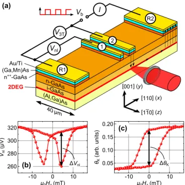
The sample layout and the measurement techniques are sketched in Fig. 1(a). Two heterostructure wafers A and B are used in our paper. The semiconductor layers are grown by molecular-beam epitaxy (MBE) on a semi-insulating GaAs(001) substrate. The layer sequence starts with a 1000-nm-thick GaAs/(Al,Ga)As superlattice (not shown), followed by 75-nm (Al0.33Ga0.67)As, a Si δ-doping layer, 50-nm (Al0.33Ga0.67)As, 50-nm i-GaAs, 100-nm n-GaAs (n=7×1016 cm−3 for sample A and n=1.2×1017cm−3
for sample B), a 15-nm-thick n→n++ transition layer, and 8-nmn++-GaAs withn=5×1018 cm−3. The top layer of 50-nm (Ga0.95Mn0.05)As is grown using low-temperature MBE. Additionally, a layer of 2.2-nm (Al0.33Ga0.67)As was grown in between then++-GaAs and the (Ga,Mn)As layers to prevent diffusion of Mn atoms into the underlyingn-GaAs layers. Thep-type (Ga,Mn)As and then-GaAs layers form an Esaki diode structure, enabling tunneling of spin-polarized carriers between (Ga,Mn)As and GaAs. The 2DEG is confined at the GaAs/(Al,Ga)As interface as depicted in Fig. 1(a) (red layer).
A chemical wet etching technique is used to confine the electron transport to a 50-μm-wide and a 750-μm-long channel oriented along the [110] direction. Contacts are defined by standard optical and electron-beam lithography techniques and evaporation of Ti/Au pads. The center spin injector contacts have varying widths between 0.5 and 4μm.
Two (90×90)-μm2 large contacts at the ends of the channel [labeled withR1 andR2 in Fig.1(a)] are used as references.
In a last etching step the (Ga,Mn)As andn++-GaAs layers in between the contacts are removed. The etching depth is a critical parameter to obtain a good 2DEG. It is chosen deep enough to ensure a complete depletion of the bulk carrier density above the 2DEG, which is confirmed by magneto- transport measurements. In many cases the 2DEG itself is also depleted or has only a small carrier density after this etching process. However, it can be repopulated by illuminating the sample, which transfers carriers from the δ-doping layer to the GaAs/(Al,Ga)As interface. Magnetotransport experiments on such carefully illuminated samples indicate the presence of a pure 2D transport in the channel without any bulk carrier conductance above the 2DEG. Directly underneath the contacts the highly doped layers form bulk-like electronic states in addition to the 2D electronic states, which ensure an efficient charge transport between the (Ga,Mn)As and the 2DEG as discussed in Ref. [5]. Finally, the sample is cleaved in the [110] direction along the transport channel, reducing the channel width to 40μm. This exposes the (110) surface, which enables direct magneto-optical access to the spin accumulation underneath the injecting contacts [10–13].
FIG. 1. (a) Sample layout and measurement techniques. (b) Nonlocal voltage Vnl as a function of the applied magnetic field HzforVb= +0.75 V. The amplitude of the spin valve signalVnl
is a measure for the spin polarization. (c) Kerr rotation θK in the 2DEG channel as a function of the applied magnetic fieldHz for Vb= +0.75 V. The height of the hysteresis loop θK is strictly proportional to the injected spin polarization.
We investigate samples from two different wafers, called sample Aand sampleB in the following. Magnetotransport measurements prove the formation of a high quality 2DEG at the GaAs/(Al,Ga)As interface for both samples with a carrier density ofn=2.3×1011cm−2, an electron mean-free path of lmf=4μm, and an electron diffusivity ofDe=4200 cm2/s for sample A and n=1.8×1011cm−2, lmf=1.5μm, and De=1300 cm2/s for sampleB.
For the measurements the samples are mounted in vacuum on the cold finger of a He flow cryostat. All experiments are performed at a temperature of∼10 K. A spin imbalance in the heterostructure can be generated by applying a bias voltageVb between one of the narrow contacts and a reference contact.
The injected spin accumulation spreads from the injector to a nearby detector contact where it generates a nonlocal voltage signalVnl via spin-charge coupling [14]. Figure1(b) shows the magnetic field dependence of Vnl using a 2-μm- wide contact as the injector and the neighboring 1-μm-wide contact as the detector (injector-detector distance of 3μm).
The value of the nonlocal voltage depends on the relative orientation of the magnetizations of injector and detector contacts. In the present case the two contacts have very similar coercive forces. Therefore, the measurement does not show the expected rectangular form as typically observed in spin valve experiments nor the maximum achievable amplitude.
However, the detected amplitude of the spin valve signalVnl is still a good relative measure for the spin polarization in the heterostructure. To increase the signal-to-noise ratio lock-in detection is utilized.
For the optical measurements of the electron spin polariza- tion we employ scanning Kerr microscopy at the cleaved edge of the sample using a cw diode laser with a power of∼10μW and a laser spot diameter of∼680 nm. A square-wave bias voltage alternating between zero andVb is applied between one of the center contacts and one of the reference contacts, and the polar magneto-optic Kerr effect (pMOKE) is measured via lock-in detection using a Wollaston prism and balanced photodiodes. The bias modulation ensures that the (quasistatic) magnetization of the (Ga,Mn)As contacts does not contribute to the Kerr rotation [10–13]. Figure 1(c) shows the Kerr rotation angleθKas a function of magnetic fieldHzwith the laser spot being located on the transport channel next to a 2-μm-wide injector contact. The measurement was performed on the diffusion side at a distance of 3μm from the injector contact. The fact that the (Ga,Mn)As-hysteresis loop can be measured at a distance of 3μm from the injector is direct proof for spin injection into the semiconductor heterostructure. To further eliminate any electro-optical contribution to the Kerr signal we evaluate the difference of both remanentθKvalues θKas a measure for the spin polarization [10–13].
III. OPTICAL PROPERTIES
Performing optical measurements on the present het- erostructure is not as straightforward as performing pMOKE measurements on bulk-GaAs samples as was performed in our previous work [10–13]. The reduced symmetry of the 2DEG might have a severe influence on the optical selection rules and therefore on the strength of the pMOKE. Indeed, it has been shown that in narrow (some 10-nm-wide) GaAs/(Al,Ga)As quantum well (QW) systems the confinement potential forces both the orbital angular momentum and the spin angular momentum of the heavy-hole states in the valence band into an out-of-plane direction perpendicular to the QW plane [15,16].
Furthermore, the confinement lifts the degeneracy of the heavy- and light-hole states at the point, shifting the light-hole band to lower energies. Taking both into account, only the out-of-plane polarized heavy holes can contribute to recombination processes with electrons in the conduction band. This has substantial consequences for magneto-optical processes. In the case of an in-plane polarized electron spin polarization (which is what we have in our experiment) angular momentum conservation prohibits the recombination of an electron with a heavy hole under emission of circularly polarized light with a well-defined helicity. Instead, only linearly polarized light will be detectable.
This effect has been verified in spin-light-emitting-diode experiments by a direct comparison of the circular polarization of the electroluminescence in top emission (with the electron spin polarization oriented perpendicular to the QW) and edge emission (with the electron spin polarization in the plane). For 10- and 15-nm-wide QWs no significant circular polarization was found with the edge-emission geometry, although a strong signal was measured in top emission [17,18].
For wide (bulk-like) QWs (d50 nm), however, a circular polarization can even be detected in edge emission, indicating that the heavy-hole spin obtains in-plane components due to the weakened quantum confinement compared to narrow QWs [16,18]. So, for wide GaAs/(Al,Ga)As-QW systems
the optical selection rules should still allow magneto-optical effects but with a reduced efficiency compared to bulk GaAs.
The heterostructure used in our experiments does not use a QW to create the 2D electron system. Instead, it uses a GaAs/(Al,Ga)As interface to produce an inverted 2DEG.
In this system only the electrons in the conduction band are confined within a triangular potential well; the holes in the valence band are not confined at all, except for the (Al,Ga)As barrier right at the interface. Therefore, neither is the degeneracy of the light and heavy holes at thepoint lifted, nor is there a confinement which forces the hole spins in the out-of-plane direction. The holes will behave like ordinary bulk holes. Hence, the optical selection rules in our system will be qualitatively unchanged with respect to bulk GaAs, and the magneto-optical Kerr effect in edge emission will be significant.
Apart from the difficulty to detect a sizable pMOKE signal originating from a narrow 2D channel, laser illumination additionally disturbs the electronic system in two ways. First, it continuously creates electron-hole pairs within the GaAs layers above the 2DEG, which increases the carrier densities within the 2DEG channel and the n-doped GaAs region underneath the spin injecting contacts. However, a simple estimation shows, that for wavelengths820 nm this optically created additional electron density lies well below the electron density of the 2DEG, and therefore this effect should have a negligible influence on the electron distribution of the system.
Considering a recombination lifetime in n-GaAs of about 1 ns, in equilibrium between electron-hole pair generation and relaxation, we can roughly estimate the additionally generated electron density in the conduction band for the used laser power of 10μW to be on the order of∼1014to∼1015 cm−3, which is well below the metal-to-insulator transition of GaAs.
So, optical generation of carriers in then-GaAs above the 2D channel will not play an important role next to the contacts where the bulk electrons have been depleted by chemical etching; bulk carriers will only be present directly underneath the spin injecting contacts.
The second effect, which plays a more severe role for the present system, is the persistent photoeffect [19–23]. The persistent photoeffect has its origin in the photoexcitation of deep impurity levels (DX centers) in the (Al,Ga)As layer. Photon absorption excites electrons into the (Al,Ga)As conduction band and hence leads to an increased conductivity, which persists even after switching off the light source since the electrons cannot return to the traps at low temperatures due to a repulsive energy barrier. Therefore, laser illumination of the sample creates an additional parasitic transport channel in theδ-doping region of (Al,Ga)As. However, magnetotransport measurements show that this parallel channel in (Al,Ga)As does not destroy the 2DEG at the GaAs/(Al,Ga)As interface as the illuminated sample still exhibits clear Shubnikov–de Haas oscillations. We conclude that transport in the illumi- nated sample can be described as parallel transport in the 2DEG and the (Al,Ga)As channel. However, transport should still be dominated by the 2DEG due to its high mobility of 5×105cm2V−1s−1 (Sample A) and 2×105 cm2V−1s−1 (Sample B). Note that the I-V characteristics of the spin injecting contacts do not change under illumination, which
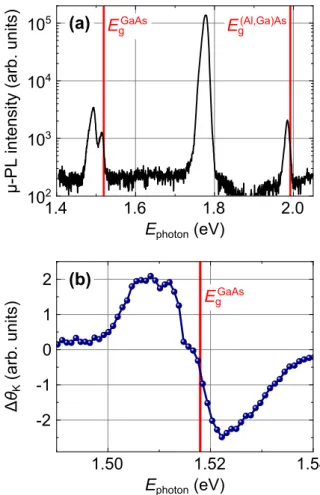
FIG. 2. (a) Microphotoluminescence measurement of the top- most layers of the heterostructure. (b) Kerr rotation spectrum in the transport channel measured under spin extraction conditions.
suggests that the process of spin injection itself is unaffected by laser illumination.
In order to characterize the optical properties of the heterostructure we perform microphotoluminescence (μ-PL) measurements at the cleaved edge of the sample. Theμ-PL spectrum of the transport channel clearly reveals three optically active regions in the sample [see Fig. 2(a)]: On one hand one observes the GaAs and the (Al,Ga)As layers with recombination peaks in the vicinity of the corresponding band gaps. On the other hand there is a strong peak at Ephoton≈1.78 eV, which stems from the superlattice grown between the substrate and the (Al,Ga)As. The latter does not contribute to charge (and hence to spin) transport and thus does not play a role for the electrical and magneto-optical investigations of the spin accumulation in the system. The luminescence peak at Ephoton≈1.98 eV mainly originates from transitions in theδ-doping area of the (Al,Ga)As and therefore represents the parallel parasitic transport channel.
Theμ-PL feature at the GaAs band gap consists of two single peaks. Here, the lower-energy peak is the well-known carbon band in GaAs [24,25]. This peak mainly stems from carbon impurities in the GaAs substrate as it is significantly weaker in the topmost MBE-grown layers compared to the GaAs substrate. The higher-energy peak at the GaAs band gap is, in part, due to excitons which are bound to Si donors in the
GaAs, but it also stems from optical transitions between the 2DEG and the valence band.
With our magneto-optical spin detection approach it should be easy to distinguish the spin accumulation in the 2DEG from a possible spin signal in the parallel transport channel within the (Al,Ga)As layer by simply tuning the laser to the GaAs band gap. Figure 2(b) displays a Kerr rotation spectrum measured at the cleaved edge in the transport channel underneath a narrow contact under spin extraction conditions. The Kerr signal is only nonzero in the vicinity of the GaAs band gap, and therefore, it can clearly be attributed to the spin polarization in the GaAs-based 2DEG.
A possible spin accumulation in the (Al,Ga)As-based parallel transport channel does not contribute to the Kerr rotation at these photon energies as the corresponding band gap is much larger and would only create a significant Kerr rotation near Ephoton≈1.98 eV. Therefore, for the Kerr measurements of the spin polarization we choose a photon energy of 1.503 eV.
Here, on one hand the influence of the laser on the electronic system in the GaAs is reduced to a minimum as the photon energy lies below the band gap, and on the other hand we can rule out any Kerr signal originating from the parasitic transport channel underneath the 2DEG.
IV. SPIN DISTRIBUTION
Figure3illustrates line scans of the Kerr rotation along the 2DEG channel forVb= ±0.75 V in sampleB, representing the spatial spin distribution within the 2DEG. The bias voltage is applied between the 2-μm-wide contact atx =0 and the large reference contact on the right-hand side of Fig.1(a). For positive voltages electrons flow from the right into the contact atx =0, creating a spin accumulation within the 2DEG by majority spin extraction; for negative voltages electrons flow from the contact to the right, injecting majority spins at the contact position. In both cases the spin polarization exhibits a sharp peak right at the position of the injector contact. The decay of the Kerr rotation signal on the left-hand side can
FIG. 3. Kerr rotation scans along the 2DEG channel for spin injection (Vb= −0.75 V) and spin extraction (Vb= +0.75 V) in sampleB. The bias voltage is applied between the 2-μm-wide contact atx=0μm and the reference contact on the right-hand side. The contacts are indicated by shaded regions. The red and orange lines represent exponential fits to the data in the field-free region with the corresponding values of the spin decay lengthsλs. The inset illustrates the current path within the sample.
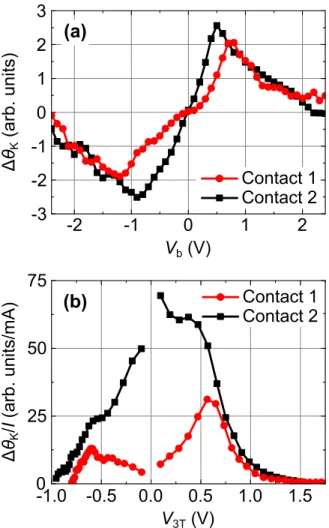
FIG. 4. (a) Bias dependence of the Kerr rotation signalθK for two different contacts of sampleA. (b) Kerr rotation normalized to the currentIplotted vsV3Tfor the same contacts as in (a).
be well fitted by an exponential in both cases, yielding spin decay lengths in the field-free regions of λs =(2.0±0.2) andλs=(1.8±0.2)μm, respectively. On the right-hand side of the contacts one has to consider a superposition of spin diffusion and drift. Therefore, the decay length is reduced (enhanced) for spin extraction (injection), which is clearly visible in our measurements.
V. BIAS DEPENDENCE
The bias dependence of the spin polarization in the het- erostructure is shown in Fig.4(a)for two different 4-μm-wide injector contacts of sampleA. In both cases the Kerr signals are measured in the transport channel directly underneath the contacts. The curves exhibit an almost perfectly antisymmetric shape with the expected sign reversal when passing from spin injection to spin extraction. However, in contrast to contact 2, contact 1 exhibits a clear nonlinearity for small bias voltages.
The discrepancy between the two contacts becomes even more pronounced when normalizing the data with respect to the current I flowing in the device and when plotting the normalized data vs the three-terminal voltage V3T, which is shown in Fig.4(b). Here, contact 2 exhibits a maximum signal at V3T=0 which monotonically decreases with increasing
|V3T|, whereas contact 1 has two maxima atV3T≈ ±0.6 V and a minimum signal atV3T=0. The nonmonotonic behavior of contact 1 strikingly resembles the bias dependence which has been reported by Oltscheret al.on similar samples where it was detected electrically in a nonlocal geometry [5]. There, the peaks at V3T≈ ±0.6 V have been linked to a signal enhancement which occurs due to direct ballistic tunneling of spin-polarized carriers from (Ga,Mn)As to the 2DEG or vice versa. Recently, a signal enhancement in a truly 2D geometry has been explained theoretically by introducing a ballistic contribution to the spin chemical potential and solving the corresponding spin ballistic-diffusion equations [6]. It has been argued that for optically injected spin polarizations such an enhancement should not be observable due to the absence of ballistic tunneling during optical orientation. Therefore, the experimentally observed nonmonotonic bias dependence of the spin polarization is a clear signature that our magneto- optical approach is sensitive to the electrical spin injection into the 2DEG.
Contact 2 shows a different bias dependence with a maximum at V3T=0. The origin of this maximum is most probably the contribution of bulk-like electronic states in the highly n-doped GaAs layers right underneath the injector contact, which increase the total Kerr rotation. The spin accumulationμs in the nonmagnetic material is proportional to its resistivity [7–9], i.e., in the case of the electronic states within the bulk-n-GaAs one hasμs ∝ρNwith the resistivity ofn-GaAs, ρN, whereas for the 2D channelμs∝Rs applies withRs being the sheet resistance of the 2DEG. Hence, due to the large resistance ofn-GaAs with respect to the 2DEG, a sizable spin accumulation can build up in the highlyn-doped GaAs layers underneath the contacts. However, the kinks in the black curve in Fig.4(b)atV3T≈ −0.5 andV3T≈ +0.3 V and the fact that the data for both contacts merge for voltages
|V3T|>0.6 V show that the bias dependence of contact 2 still contains the contributions from the pure 2D spin polarization.
Note that these subtle differences in the bias dependence of different (but nominally same) contacts can be detected in our magneto-optical experiments but are difficult to extract from all-electrical measurements.
All in all, these measurements show that the magneto- optical detection method is sensitive to the 2D spin accumula- tion. However, as shown by the signal below contact 2, directly underneath the spin injecting contacts the bulk-like electronic states within the highlyn-doped GaAs layers might become visible as an additional contribution to the optically detected spin signal. Note that this bulk carrier distribution is only present directly underneath the injector contacts; in between the contacts it has been completely removed by wet-chemical etching. Hence, Kerr rotation signals, which are detected next to the contacts, stem solely from the 2D spin accumulation.
VI. HANLE MEASUREMENTS
Finally, we perform Hanle depolarization measurements to investigate the dynamical aspects of the 2D spin injection. Note that we use for all of our Hanle measurements a measurement protocol in which the magnetization of the sample is reversed every∼5 s. Therefore, dynamic nuclear polarization (DNP)
effects, which are frequently observed in Hanle measurements, are eliminated in our experiment.
Spin relaxation in GaAs-based 2DEGs is typically governed by the D’yakonov-Perel’ mechanism [26,27], just like in bulk GaAs; hence, in the motional narrowing limit, the relation 1/τs∝ 2kτp is valid, whereτs andτp are the spin and momentum relaxation times, respectively, andk is the momentum-dependent Larmor precession frequency arising from spin-orbit interaction. Since spin-orbit coupling in quantum confined systems is usually much larger than in bulk materials, spin relaxation in our 2DEG is expected to be more effective than in bulk GaAs. Moreover, the long momentum relaxation times in our high-mobility 2DEG samples should additionally contribute to an efficient D’yakonov-Perel’ spin relaxation.
Contrary to bulk GaAs spin relaxation in two-dimensional systems shows a pronounced anisotropy [28,29]. The lifetime of an electron’s spin in a 2DEG strongly depends on the spin-polarization direction with respect to the spin-orbit- coupling fields. The spin-orbit fields in a (001)-grown 2DEG are oriented in the quantum confinement plane. Thus, a spin polarization perpendicular to the 2DEG plane experiences a strong spin-orbit torque, and accordingly the spin relaxes very rapidly with spin lifetimes on the order of 100 ps [30–32].
In the present experiment the injected spin accumulation is polarized in the quantum confinement plane. For this case a giant spin-relaxation anisotropy has been predicted [28,29]
with a large spin-relaxation rate for electron spins polarized along the [110] direction and a small spin-relaxation rate for a spin ensemble pointing in the [110] direction. Indeed, it has been shown that the D’yakonov-Perel’ mechanism is strongly suppressed for a spin polarization along the [110]
crystallographic direction with spin lifetimes ranging from a few to several tens of nanoseconds, whereas the spin lifetime for a spin ensemble along the [110] direction typically remains in the subnanosecond regime [30,33,34].
The spin-relaxation anisotropy within the (001) crystallo- graphic plane has direct consequences on the Hanle experi- ments performed in this paper. For the Hanle measurements we apply the magnetic field along the [001] direction. The spin accumulation precesses in the (001) plane and probes all relaxation times in the different in-plane directions. Thus, the spin lifetimeτsextracted from our Hanle curves is given by the geometric mean of the spin lifetimes along the two principal axes [110] and [110] [29,34],
τs =
τs,[110]τs,[110],
where τs,[110] and τs,[110] are the spin-relaxation times for electron spins polarized along the [110] and [110] directions, respectively.
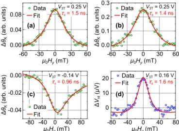
Figures5(a)and5(b)display Hanle depolarization curves for both contacts of sample A, measured on the diffusion side 1μm away from the injecting contact in each case to rule out any influence of the injector contacts on the spin polarization. Although the large electron mean-free path of a few micrometers suggests that the system has to be considered to be in a crossover regime between ballistic and diffusive transports, the data can be well modeled using the standard drift-diffusion theory of spin injection. A fit of the data yields
FIG. 5. (a) and (b) Hanle depolarization curves of sampleAfor both contacts of Fig.4using magneto-optical detection. The fits yield spin lifetimes of (a) (1.5±0.1) ns for contact 1 and (b) (1.4±0.2) ns for contact 2. (c) Hanle depolarization curve of sampleBusing optical detection. The fit yields a spin lifetime of (0.96±0.09) ns. (d) Hanle depolarization curve of sampleBusing nonlocal detection (no laser illumination). The fit yields a spin lifetime of (1.6±0.5) ns.
spin lifetimes of τs =(1.5±0.1) and τs=(1.4±0.2) ns, respectively. Figure 5(c) shows a Hanle curve from sample B. For this measurement the distance between the injector and the laser spot is chosen to be 3μm. Again, the fit yields a spin lifetime on the order of 1 ns.
To rule out that the spin accumulation is affected by opti- cally generated charge carriers, we also perform all-electrical nonlocal Hanle measurements without laser illumination on the cleaved edge. In these measurements neither do we have optically generated electron-hole pairs in the n-GaAs, nor are the (Al,Ga)As DX centers excited. Again the Hanle depolarization curve, which is free of DNP effects, can be well modeled with the diffusive theory [see Fig.5(d)]. The fit yields a spin lifetime ofτs=(1.6±0.5) ns, in good agreement with the optically detected spin lifetimes.
Recently, the spin lifetime in a similar sample has been calculated using the expressionλs =√
Deτswith the electron diffusivity De determined from magnetotransport measure- ments and the spin decay length λs extracted from nonlocal spin valve measurements [5]. This simple estimation led to a spin lifetime in the range of a few tens of picoseconds, in accordance with former spin lifetime measurements of 2D electron systems confined in GaAs(001)-based quantum well structures [2,30–32]. However, when performing Hanle experiments Oltscher et al. were able to detect nonlocal depolarization curves suggesting spin lifetimes in the range of a few nanoseconds [5], which is comparable to the present measurements. In Ref. [5] the observed Hanle signals have been linked to DNP effects appearing for certain bias conditions. However, as mentioned above, DNP cannot arise in the present experiment, nor do we see a pronounced bias dependence of τs. To resolve the discrepancy between the spin lifetimes estimated via λs =√
Deτs and the lifetimes resulting from Hanle measurements one can consider two possible explanations:
First, as has already been pointed out in Ref. [5], the standard diffusive model of spin injection [7–9] might be unsuitable to describe high-mobility 2D systems. In the case of Oltscheret al., evaluating the data with the diffusive theory resulted in unphysical spin injection efficiencies larger than 100%. It has been argued that the standard model cannot be applied to samples with ballistic transport properties [5].
Therefore, naively modeling our Hanle data with the standard model might lead to artificially enhanced spin lifetimes as the theory does not take into account the (quasi)ballistic transport between injection and detection positions. However, it seems unlikely that ballistic effects play a crucial role in our Hanle measurements. In contrast to the process of spin injection, which is affected by ballistic tunneling [5], spin transport along the 40-μm-wide transport channel should already exhibit diffusive transport characteristics. Thus, the Hanle effect, which is detected at a distance of a few micrometers to the injector contact, should still be governed by the spin drift-diffusion equations, which is further supported by the fact that the measured Hanle line shapes can be well modeled with the diffusive theory (see Fig.5).
The second more likely explanation for the difference between the spin lifetimes extracted from Hanle measurements and the lifetime estimation of Ref. [5] is the fact that the expressionλs=√
Deτsmight not be applicable in the case of a 2D electron system. Indeed, it has been argued that the high electron-electron-scattering rates in high-mobility 2DEGs can lead to a reduction of the spin diffusivity Ds with respect to the charge diffusivityDe[35,36], resulting in an enhanced spin-relaxation time [37]. Therefore, spin relaxation is affected byDsrather thanDe, suggesting thatλs =√
Dsτs should be the correct link betweenλs andτs. Using this expression we estimate a value for the spin diffusivityDs ∼40 cm2/s, which is two orders of magnitude smaller than the charge diffusivity De. A comparable reduction of Ds with respect to De has already been observed in Refs. [34,38–40].
VII. CONCLUSIONS
To summarize, we have investigated electrical spin injection into a GaAs-based high-mobility 2DEG by using electrical and optical measurement techniques. Similar to the data presented in Ref. [5] we find a signal enhancement in the bias dependence that may be attributed to a ballistic contribution to the injection process. Both detection methods independently show a clear Hanle depolarization, suggesting averaged in-plane spin lifetimes on the order of 1 ns. These spin lifetimes can be understood by considering a spin diffusivityDs which is significantly smaller than the charge diffusivityDe. Clearly a more thorough theoretical investigation of spin injection into and transport in 2DEG systems is required to explain the influence of electron-electron interactions possibly enhancing spin lifetimes as suggested in Ref. [37]. In general, there is a need to extend the standard spin drift-diffusion model to the (quasi)ballistic case.
ACKNOWLEDGMENT
Financial support by the Deutsche Forschungsgemeinschaft via Grant No. SFB 689 is gratefully acknowledged.
[1] S. Datta and B. Das,Appl. Phys. Lett.56,665(1990).
[2] P. R. Hammar and M. Johnson,Phys. Rev. Lett.88,066806 (2002).
[3] H. C. Koo, J. H. Kwon, J. Eom, J. Chang, S. H. Han, and M.
Johnson,Science325,1515(2009).
[4] R. Jansen, B.-C. Min, and S. P. Dash,Nat. Mater.9,133(2010).
[5] M. Oltscher, M. Ciorga, M. Utz, D. Schuh, D. Bougeard, and D. Weiss,Phys. Rev. Lett.113,236602(2014).
[6] K. Chen and S. Zhang,Phys. Rev. B92,214402(2015).
[7] A. Fert and H. Jaffr`es,Phys. Rev. B64,184420(2001).
[8] E. I. Rashba,Eur. Phys. J. B29,513(2002).
[9] J. Fabian, A. Matos-Abiague, C. Ertler, P. Stano, and I. ˇZuti´c, Acta Phys. Slov.57,565(2007).
[10] P. Kotissek, M. Bailleul, M. Sperl, A. Spitzer, D. Schuh, W.
Wegscheider, C. H. Back, and G. Bayreuther,Nat. Phys.3,872 (2007).
[11] B. Endres, F. Hoffmann, C. Wolf, A. Einwanger, M. Utz, D.
Schuh, G. Woltersdorf, M. Ciorga, D. Weiss, C. H. Back, and G. Bayreuther,J. Appl. Phys.109,07C505(2011).
[12] B. Endres, M. Ciorga, R. Wagner, S. Ringer, M. Utz, D. Bougeard, D. Weiss, C. H. Back, and G. Bayreuther, Appl. Phys. Lett.100,092405(2012).
[13] B. Endres, M. Ciorga, M. Schmid, M. Utz, D. Bougeard, D.
Weiss, G. Bayreuther, and C. H. Back,Nat. Commun.4,2068 (2013).
[14] M. Johnson and R. H. Silsbee,Phys. Rev. Lett.55,1790(1985).
[15] R. W. Martin, R. J. Nicholas, G. J. Rees, S. K. Haywood, N. J.
Mason, and P. J. Walker,Phys. Rev. B42,9237(1990).
[16] S. A. Crooker, D. D. Awschalom, J. J. Baumberg, F. Flack, and N. Samarth,Phys. Rev. B56,7574(1997).
[17] R. Fiederling, P. Grabs, W. Ossau, G. Schmidt, and L. W.
Molenkamp,Appl. Phys. Lett.82,2160(2003).
[18] O. M. J. van ’t Erve, G. Kioseoglou, A. T. Hanbicki, C. H. Li, and B. T. Jonker,Appl. Phys. Lett.89,072505(2006).
[19] A. Kastalsky and J. Hwang, Solid State Commun. 51, 317 (1984).
[20] M. I. Nathan,Solid State Electron.29,167(1986).
[21] D. J. Chadi and K. J. Chang,Phys. Rev. Lett.61,873(1988).
[22] D. J. Chadi and K. J. Chang,Phys. Rev. B39,10063(1989).
[23] P. M. Mooney,Semicond. Sci. Technol.6,B1(1991).
[24] G. B. Stringfellow, W. Koschel, F. Briones, J. Gladstone, and G.
Patterson,Appl. Phys. Lett.39,581(1981).
[25] L. Pavesi and M. Guzzi,J. Appl. Phys.75,4779(1994).
[26] M. I. D’yakonov and V. I. Perel’, Sov. Phys. JETP33, 1053 (1971) [Sov. Phys. Solid State13, 3023 (1972)].
[27] M. I. D’yakonov and V. Y. Kachorovskii, Sov. Phys. Semicond.
20, 110 (1986).
[28] N. S. Averkiev and L. E. Golub,Phys. Rev. B60,15582(1999).
[29] N. S. Averkiev, L. E. Golub, and M. Willander, J. Phys.:
Condens. Matter14,R271(2002).
[30] Y. Ohno, R. Terauchi, T. Adachi, F. Matsukura, and H. Ohno, Phys. Rev. Lett.83,4196(1999).
[31] D. Stich, J. Zhou, T. Korn, R. Schulz, D. Schuh, W. Wegscheider, M. W. Wu, and C. Sch¨uller, Phys. Rev. Lett. 98, 176401 (2007).
[32] V. Lechner, L. E. Golub, F. Lomakina, V. V. Bel’kov, P. Olbrich, S. Stachel, I. Caspers, M. Griesbeck, M. Kugler, M. J. Hirmer, T. Korn, C. Sch¨uller, D. Schuh, W. Wegscheider, and S. D.
Ganichev,Phys. Rev. B83,155313(2011).
[33] D. Stich, J. H. Jiang, T. Korn, R. Schulz, D. Schuh, W.
Wegscheider, M. W. Wu, and C. Sch¨uller, Phys. Rev. B76, 073309(2007).
[34] R. V¨olkl, M. Schwemmer, M. Griesbeck, S. A. Tarasenko, D.
Schuh, W. Wegscheider, C. Sch¨uller, and T. Korn,Phys. Rev. B 89,075424(2014).
[35] I. D’Amico and G. Vignale,Phys. Rev. B62,4853(2000).
[36] I. D’Amico and G. Vignale,Europhys. Lett.55,566(2001).
[37] W. J. H. Leyland, G. H. John, R. T. Harley, M. M. Glazov, E. L.
Ivchenko, D. A. Ritchie, I. Farrer, A. J. Shields, and M. Henini, Phys. Rev. B75,165309(2007).
[38] C. P. Weber, N. Gedik, J. E. Moore, J. Orenstein, J. Stephens, and D. D. Awschalom,Nature (London)437,1330(2005).
[39] L. Yang, J. D. Koralek, J. Orenstein, D. R. Tibbetts, J. L. Reno, and M. P. Lilly,Nat. Phys.8,153(2012).
[40] P. Altmann, M. Kohda, C. Reichl, W. Wegscheider, and G. Salis, Phys. Rev. B92,235304(2015).