Hanle spin precession in a two-dimensional electron system
T. Kuczmik, M. Oltscher, A. Bayer, D. Schuh, D. Bougeard, M. Ciorga,*and D. Weiss Institute for Experimental and Applied Physics, University of Regensburg, D-93040 Regensburg, Germany
(Received 3 March 2017; revised manuscript received 3 May 2017; published 25 May 2017)
We investigate the nonlocal Hanle effect in high mobility two-dimensional electron systems using (Ga,Mn)As/GaAs spin Esaki diodes as spin selective contacts. Spin signals in these systems can be strongly affected by dynamic nuclear polarization, which mimics long spin-relaxation times extracted from the measured Hanle curves. Here, we introduce a method which largely suppresses these effects by using an ac injection-detection setup. This allows us to extract from the measurements realistic spin lifetimes on the order of single nanoseconds. As the detection of Hanle signals is also strongly affected by offset signals we discuss the magnetic field dependence of these background voltages observed in lateral nonlocal spin injection devices.
We show how the strength of the background magnetoresistance can be minimized by choosing a proper device geometry.
DOI:10.1103/PhysRevB.95.195315
I. INTRODUCTION
Electrical spin injection into a two-dimensional electron system (2DES) confined in a semiconductor structure is a prerequisite for the realization of spin injection devices with many new functionalities [1], with the Datta-Das spin field effect transistor [2] being a primary example. Whereas spin injection into bulk semiconductors has been realized in many systems [3–8], there are few reports of successful experiments in 2D systems [9], particularly in those with high mobility carriers. [10,11] Therefore, many spin properties of semiconductor 2DESs have been investigated so far using optical methods, taking advantage of optical orientation in such systems [12–14]. Recent successful experiments demon- strating spin injection in 2DESs in InGaAs quantum wells and at a GaAs/(Al,Ga)As interface [9,11] open up novel ways to study these phenomena in a lateral geometry, typical for potential devices. One of the most important spin parameters of the transport channel is the spin-relaxation timeτs, which determines how far and how efficiently spin information can be transported along the channel. Spin dynamics is typically studied using the Hanle effect, i.e., precession of spins in a magnetic field transversal to the initial spin direction [15]. It was discussed before that Hanle experiments on 2D systems can be problematic [16]. As τs is usually of the order of picoseconds in high mobility 2DESs [1], a relatively large magnetic field B is required to induce spin precession. In materials with large spin-orbit coupling, preferable for spin manipulation, this field is even larger because of the spin-orbit effective magnetic field. This is not particularly desirable, as a large B can affect the magnetization of the spin-aligning contacts, thus distorting Hanle measurements. Recently, we briefly discussed Hanle curves measured in a 2D channel by means of a fully electrical setup, which were found to be strongly bias dependent [11]. What is more, from the measure- ments we extracted a spin-relaxation time ofτs=5 ns, larger than expected from a pure Dyakonov-Perel spin-relaxation mechanism [1,17,18], dominating in semiconductor 2DESs.
We linked such a behavior to dynamic nuclear polarization
*Corresponding author: mariusz.ciorga@ur.de
(DNP) effects, often visible in spin injection experiments in GaAs-based systems, which can strongly affect the Hanle signal, leading to wrong values for the extracted parameters.
In another work, however, using optical methods and making sure to avoid DNP effects, we also measured spin-relaxation times on the order of 1 ns [19]. It is then clear that it is very desirable to optimize Hanle experiments in order to be able to extract spin injection parameters with large reliability.
Here, we discuss electrical Hanle measurements on a series of 2DES samples, focusing on two issues: (i) the narrowing of Hanle curves as a result of DNP effects and (ii) the large magnetic field dependence of the nonlocal background voltage, that typically obscures the Hanle spin signal. We show that problem (i) can be solved by using a low excitation ac technique, that suppresses buildup of a nuclear magnetic field. The problem (ii) can be overcome by choosing a large aspect ratioL/w, withLthe injector-detector separation and w the width of the channel. Avoiding both DNP and large background signals allows us to derive reliable spin-relaxation timesτs for 2DESs from our all-electrical measurements. We have obtainedτsvalues between 0.8 and 2.5 ns, with the larger spin-relaxation times measured for the narrower channels.
II. EXPERIMENTAL TECHNIQUES A. Sample layout
The investigated samples were grown by molecular beam epitaxy on a semi-insulating GaAs-(001) substrate. A sketch of the wafer layout is shown in Fig.1(b). The two-dimensional electron system is confined at the (Al,Ga)As (thicknesst = 125 nm)/GaAs (t=50 nm) interface and charge carriers are provided by a Si-δ doping layer in the (Al,Ga)As region. A moderately n-doped layer of GaAs (n=6×1016cm−3,t= 100 nm) is grown on top of these layers. The top lay- ers, consisting of an n-GaAs → n+-GaAs transition layer (t=15 nm,n+=5×1018cm−3), a highly n+-doped GaAs layer (t=8 nm,n+>1019cm−3), and 50-nm ferromagnetic (Ga,Mn)As (p++≈1020cm−3), form a highly asymmetricp-n junction which works as a spin Esaki diode [5,20–22]. Apart from the degenerately dopedp-type (Ga,Mn)As layer with a Mn concentration of typically 5.6% and a Curie temperature
-10 -8 -6 -4 -2 0 2 4 6 8 10 -30
-20 -10 0 10 20 30
ρxx (kΩ)
Bz (T) RH(kΩ)
0 1 2
… R2
R1
NL 3T
>>λsf >>λsf (Al,Ga)As
n-GaAs
GaAs 2DES
-doping (Al,Ga)As
n+- GaAs etch (Ga,Mn)As
n -> n+ Au / Ti
x z y
(a) (b)
-0.4 -0.2 0.0 0.2 0.4 0.6 -200
-100 0 100 200
wx= 700 nm wy= 10 µm
I (μA)
V3T (V)
(c) (d)
wy
wx
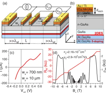
FIG. 1. (a) Sketch of a lateral spin injection device. Narrow ferromagnetic (FM) (Ga,Mn)As contacts on top of the channel are used to inject/detect spin accumulation in the 2DES. Each sample features typically two to six FM contacts with widths varying between 500 and 2000 nm. Additional contacts on both ends of the channel (R1, R2), far away from the spin aligning contacts, serve as reference. (b) Schematic of the wafer layout. (c) I-V curve of one of the spin injection contacts; the characteristic negative differential resistance dip is observed between 300 and 450 mV. (d) Typical magnetotransport traces taken from the high mobility 2DES at the inverted (Al,Ga)As/GaAs interface.
of 55 K, the Esaki diode consists of a highly Si dopedn+layer.
Doping levels of more than 1×1019cm−3we achieve by the so-called pseudo-δ doping, meaning that the growth process of the 8-nm-thickn+-GaAs layer using continuous Si flux is stopped every 1.6 nm for 10 s, to accumulate Si dopants. The highn+doping makes thep-njunction more symmetric and thus lowers its resistance.
Spin injection from (Ga,Mn)As/GaAs spin Esaki diodes can be very efficient, with spin polarization of the injected current Pinj reaching≈80% [5,23]. In these structures, spin accumulation in the n region is generated via tunneling of spin-polarized electrons between the (Ga,Mn)As valence band and the n-GaAs conduction band. When the junction is reverse biased (I <0), electrons tunnel into GaAs and spin injectionoccurs. Forward biased (I >0) electrons tunnel in the opposite direction, generating a spin accumulation with opposite orientation due tospin extraction. Tunneling is suppressed at a certain positive voltage, when the conduction- band edge on thenside is aligned with the valence-band edge on thepside. Negative differential resistance is observed as a characteristic dip in the I-V curve of a spin Esaki diode at this voltage, which can be seen in Fig.1(c)for one of the samples discussed in this paper.
The lateral two-dimensional spin transport channel is formed as a Hall bar, fabricated using standard photolithogra- phy techniques and wet-chemical or dry reactive ion etch- ing. We fabricated devices with different channel widths wy, ranging from 2.5 to 10μm, with usually four narrow
Au/Ti/(Ga,Mn)As contacts on top (wx =500 nm–2 μm) patterned by electron-beam lithography and wet chemical etching. Additionally, several large Au/Ti/(Ga,Mn)As con- tacts (A=100×100μm2) are evaporated far away from the spin injection contacts. These large contacts serve as reference electrodes in nonlocal spin injection experiments or as current or voltage leads in magnetotransport measurements. In the final step the highly doped top layers between the injector/detector contacts are partially etched away (detch =56±4 nm) to deplete the mildly dopedn-type GaAs layers and to confine (spin) transport exclusively to the 2DES. For etching we used either highly diluted phosphoric acid or acetic acid. A sketch of the sample layout for nonlocal spin injection measurements is shown in Fig.1(a). All measurements were performed at T =1.4 K.
In order to avoid an additional energy barrier between (Ga,Mn)As and the 2DES we use an inverted structure, i.e., with GaAs grown on top of (Al,Ga)As, instead of the standard (Al,Ga)As/GaAs interface. It is known that such inverted 2DES structures are often devoid of charge carriers at liquid He temperatures. In order to repopulate the 2DES with electrons we illuminate our samples with a low intensity infrared light emitting diode. This process utilizes the persistent photoconductivity effect in (Al,Ga)As, creating free charge carriers, which occupy the empty states in the 2DES [24]. As this illumination process has to be optimized for each device by varying illumination time and strength, the 2DES parameters such as charge-carrier density and sheet resistance can differ from sample to sample. All our samples show, however, clear two-dimensional transport characteristics with high mobilities (μe=250 000–500 000cmV s2), similar to the one shown in Fig.1(d).
B. Spin valve effect
The typical nonlocal spin valve (NLSV) geometry used to probe electrical spin injection is shown in Fig.1(a). One of the narrow ferromagnetic contacts is used as injector, i.e., a current is driven between this contact and the closest reference contact.
The spin accumulation generated underneath the injector diffuses along the channel. All the other ferromagnetic contacts are then used to measure the nonlocal voltage resulting from Silsbee-Johnson spin-charge coupling [25] with respect to the other reference contact. In the tunneling regime this spin-related voltage can be written as [26–28]
VNLs = PinjPdetRsI λsf 2wy
exp(−L/λsf), (1) wherePinj(det)is the injection (detection) efficiency,λsf is the spin diffusion length, and Rs is the sheet resistance of the channel. Pinj is defined as the polarization of the injected current and given by II↑−I↓
↑+I↓, where ↑ and ↓ label the two different spin species. The sign of Pinj(det) is controlled by the magnetization orientation of the corresponding contacts.
PinjPdet>0 holds for parallel (P) orientation of magnetization in the injector and detector contacts and PinjPdet<0 for antiparallel (AP) alignment.
In a typical NLSV experiment we sweep the magnetic field By along the contact between ±0.5 T, magnetic field
values large enough to orient the magnetization along the B direction. When the magnetization direction of injector and detector switches from parallel to antiparallel or vice versa (requiring different switching fields for injector and detector) the nonlocal voltage changes by|VNL| =2|VNLs |, withVNL=VNLAP−VNLP (see Fig.2). From theLdependence of the signal one can extract important spin-related parameters, like spin-flip length λsf and spin injection efficiency Pinj. In the samples presented below λsf is typically between 2 and 12μm. At low bias we obtain for our devices Pinj= 75±10%, being in a good agreement with previous reports using similar spin Esaki diodes [5,11,23].
Ideally, no charge current flows between injector and detec- tor and the measured nonlocal voltage stems solely from spin accumulation, i.e.,VNL=VNLs . In our measurements, however, similarly as in many other nonlocal experiments [28–31]
and particularly for semiconducting channels [3,5,23,32], a nonzero baseline voltageVNLbaseis detected, which constitutes an additional contribution to the measured nonlocal volt- age as VNL=VNLs +VNLbase. Although there have been some speculations about the spin-dependent origin [29] of VNLbase, two spin-independent mechanisms have been discussed in the literature as the main source of VNLbase. One is related to the electric field spreading around the injector contact, resulting from an inhomogeneous current distribution along the y direction [33]. The other contribution is caused by thermoelectrical effects at the contacts [34,35]. In general, VNLbasecan be very large [3], but in our experiments it is typically on the order of the spin signalVNLs [see Fig.2(d)] [5,11,23].
C. Hanle effect
The Hanle effect, i.e., precession and dephasing of a spin ensemble in a transverse magnetic field B [15], is another very important way of probing injected spins [25,36]. Hanle measurements constitute a direct way of extracting the spin- relaxation timeτsfrom the shape of the experimental traces. In the simplest case, ignoring drift and diffusion, the line shape is given by a LorentzianS(B)=S(0)/[1+(ωL(B)τs)2] [6,37], where S(0) is the injected spin density at zero magnetic field andωL(B)=gμ0B/¯his the Larmor frequency of spin precession. In this case τs =h/gμ¯ 0B1/2, where B1/2 is the B value corresponding to the half width at full maximum of the experimental curve. In the presence of drift or diffusion a more complex fitting procedure is required to obtain τs
[see Eq. (2)] [26], but the reciprocal relation betweenτs and the width of the curve still holds. It is worth noting that τs can also be estimated from the NLSV signal usingλs =
√Dsτs, but usually one does not know the value of the spin- diffusion constantDs, which in general is different from the charge diffusion constantDe, extracted from magnetotransport experiments [38]. This is particularly true for high mobility 2D systems, where electron-electron interaction has to be taken into account [39,40]. Thus Hanle measurements are of utmost importance to get information on spin relaxation.
In our lateral device the injected spins are collinear with the magnetization of the contact, i.e., they are lying in thexyplane of the sample. An applied out-of-plane field Bzinduces spin precession around the external field with Larmor frequency ωL. As the detector is only sensitive to spins collinear with its
-60 -40 -20 0 20 40 60 10
20 30 40 50
-60 -40 -20 0 20 40 60 0.0
0.5 1.0 1.5 2.0
-150 -100 -50 0 50 100 -1.2
0.0 1.2
-20 -15 -10 -5 0 5 10 15 20 0.0
0.2 0.4 0.6
-60 -40 -20 0 20 40 60 -5
0 5 10 15
AP
VNL (µV)
B (mT)
I=−1 µA
P (a)
-60 -40 -20 0 20 40 60 0.3
0.6 0.9 1.2 1.5
P (b) AP
VNL (mV)
B (mT) I=−70 µA
AP (c) P
VNL (mV)
B (mT)
I=+50 µA (d)
ΔVnl (Pn) Vbasenl
V (mV)
I (µA)
I=−70 µA τs=100 ns
(AP-P)/2
(f)
VNL (mV)
B (mT) I=−1 µA
(e)
VNL (µV)
B (mT) (AP-P)/2 τs=1 ns
-11 0 11
Pn(%)
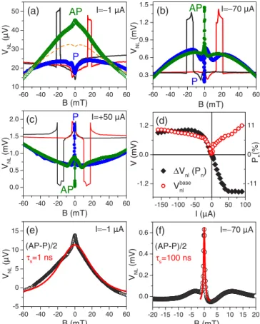
FIG. 2. dc nonlocal measurement at low (a) and at a high (b) negative bias, as well as for (c) high forward bias. Both NLSV (black and red lines) and Hanle curves (olive and blue symbols) are shown.
The dashed orange line is the magnetoresistance of the background voltage VNLbase(Bz)=(VNLAP+VNLP)/2. (d) Bias dependence of the nonlocal spin signal VNL (black diamonds) together with the corresponding nonlocal baselineVNLbasevoltage (red circles) atBz=0.
The righty axis labels the spin-density polarizationPn calculated fromVNLusing Eq. (5). (e) and (f) show Hanle curves after removing the background from the measurements shown in (a) and (b), respectively. Red solid lines are simulated Hanle curves using Eq. (2) with corresponding spin-relaxation timesτs. The measurements were performed on the sample withwy =10μm and forL=3.6μm with x[010] andy[100] crystallographic direction.
own magnetization axis, the precession causes oscillations of VNLs . Dephasing of spins as a result of diffusion between the injector and the detector leads finally toVNLs =0 at sufficiently largeBz.
Next, we describe the procedure used to measure Hanle traces. To saturate the magnetization of all contacts and to orient the injected spins along theydirection a magnetic field By= ±0.5Tis applied. For measurements in P magnetization configuration of injector and detector,Byis then swept to zero.
The AP configuration is established by sweepingBy through zero till the magnetization of one of the contacts (typically the injector) is reversed; thenByis also swept back to zero. Once the desired (P or AP) state has been prepared, the sample is rotated out of plane by 90◦and the field is swept inzdirection up toBz=0.5 T, while measuring the nonlocal voltage. Then the sample is rotated back to the original in-plane position and the procedure is repeated, but sweepingBz in opposite
direction, i.e., down to Bz= −0.5T. We avoid sweeping Bz
through zero because of the strong effects related to DNP [41–44] induced by injected electron spins. For the same reason we also wait approximately 10 min after sweepingBy
to zero and before sweepingBz, allowing the resulting nuclear field to relax [44].
To analyze the experimental data we employ a model developed in Ref. [26]. Following that model for collinear magnetization configuration of injector and detector and for the detector placed at positionx, the nonlocal voltageV(Bz), is, for the pure diffusive case (absence of drift), given by
V(Bz)=V0exp(−α1x/λsf)
α1
α21+α22cos α2
λsf
x
− α2 α12+α22 sin
α2 λsfx
. (2)
Here, V0 is the nonlocal voltage at the point of injection, x =0. The parameters α1 and α2 are given by α1=(1/√
2) 1+√
[1+(ωLτs)2] and α2= (1/√
2)
−1+√
[1+(ωLτs)2].
To take the finite dimensions of the contacts into account, Eq. (2) has to be integrated alongx over the width of injector and detector contacts. Such a formula is used to fit the experimental data and extractτs.
III. RESULTS AND DISCUSSION A. dc measurements
Measurements of spin injection are usually conducted using a dc configuration with a constant current applied between an injector and a reference contact while the nonlocal voltage is measured between a detector and the second reference contact.
Applying a dc current allows us to study the difference between injection and extraction of spins, as well as to study the influence of bias on spin injection parameters or spin dynamics.
As we discuss in this section, dc measurements are prone to accumulation of nuclear spins which affect the analysis of spin relaxation. In Fig.2we show typical NLSV and Hanle measurements for different values of the constant injection current. We show both the case of injection (I <0) and the case of extraction (I >0). As the injection process in spin Esaki diodes highly depends on the applied bias voltage [5,45], the results for both the low bias as well as the high bias regime are shown in Fig.2(a)and Figs.2(b)and2(c), respectively. In Fig.2(d)we plot the dependence of the NLSV signal amplitude VNL on the injection currentI. In agreement with Eq. (1), VNL(I) grows linearly withI for low currents, but becomes nonlinear at larger currents due to the dependence ofPinj on bias [5,45]. As expected,VNLchanges its sign on reversing the sign of the injected current. The background voltageVNLbase, also plotted in Fig.2(d), is also proportional to the injection current, but it does not change sign withI. For low current values the background signal is nearly symmetric with respect to current polarity. The small asymmetry observed for larger currents could be related to the nonlinearity of the I-V curve of the single junction [see Fig.1(c)].
For out-of-plane measurements, VNLbaseshows a strong B- field dependence, which deforms Hanle curves, especially at
lowB. The field dependence of the background can be usually well approximated by a quadratic function, as observed before for bulk devices [3,5]. To extract spin parameters, as the spin- relaxation time, one can thus not simply use the raw data for fitting Eq. (2) to the experimental data. Instead, it is necessary to remove the background before fitting. One way of doing this is to simply fit the background with a function∝B2and subtract it from both AP and P Hanle curves. The other way is to treat the background as spin independent and the same for P and AP configurations. Then the spin-independent background can be removed by subtracting both curves i.e., calculating VNLs =(VNLAP−VNLP )/2. The resulting curve can be used for fitting, whereas the corresponding baseline voltage is given by VNLbase=(VNLAP+VNLP )/2. Both methods give essentially similar results, up to the error introduced by data manipulation.
Figures 2(e) and 2(f) illustrate as an example the result of background removal for traces measured with a constant current ofI = −1 and−70μA. Comparing curves measured at high and low bias reveals another characteristic feature of dc measurements, i.e., narrowing of the Hanle curves with increasing current bias. As the width of the curves is inversely proportional toτs, the spin-relaxation time seems to depend on the applied bias. Fits to the Hanle traces in Figs. 2(e) and 2(f) give τs ≈1 ns for I = −1μA and τs ≈100 ns for I = −70μA, respectively. Furthermore, the fits are not perfect. ForI = −1μA, in particular, the experimental curve is, in contrast to the fit, asymmetric and displays a narrow peak close to zero field. The value of 100 ns measured for I = −70μA is much too large for a 2DES system [13,14,46].
We link the narrowing of the Hanle curves to dynamic nuclear polarization, discussed below.
B. Influence of DNP effects
Spin injection experiments on GaAs-based bulk devices are strongly affected by DNP effects [41,42,44,47]. These effects originate from polarization of nuclear spins by the injected electron spins via hyperfine interaction, thus resulting in an effective nuclear magnetic fieldBN(Overhauser field), which adds to the externally applied field Bext. This nuclear field contributes to the total field experienced by the electrons’ spin, which is given by Btot=Bext+BN. The nuclear magnetic field produced by flip-flop processes is, in the steady state and for small S (neglecting Knight shift and dipole-dipole interactions between nuclear spins), given by [48]
BN =f bn
S·Bext
Bext2 Bext. (3) Here, bn is the maximum possible nuclear field forming when all nuclei are uniformly polarized (for GaAsbn= −17 T) and f 1 is the leakage factor, describing nuclear spin relaxation through other mechanisms than hyperfine flip-flop processes. S stands for the mean electronic spin, generated in our experiment by spin injection, equal to 1/2 for a spin-density polarizationPn=100%. From Eq. (3) it follows that BN is always collinear with Bext, but its absolute value does not depend on the magnitude of Bext but only on the projection of Son Bext. Small in-plane components of Bext are therefore sufficient to induce a large BN. These can be stray fields from ferromagnetic contacts or fields resulting
from small misalignments of the sample in the out-of-plane field. Therefore, in standard spin injection experiments nuclear effects are particularly visible at low applied fields, when BN>Bext. In standard NLSV experiments DNP manifests itself as a depolarization peak observed when the external Bin-planeis close to zero [3,5,41,44]. Hanle curves, on the other hand, can be narrowed by the nuclear field [43], thus altering extraction of spin parameters.
According to Eq. (3), BN is directly proportional to the average spin in the channel S, given by S=1/2Pn. The spin-density polarization Pn is directly related to the spin accumulation in the channel and is, at the injection point, given by [26]
Pn0= −PinjI Rsλsf
2wy
eD(EF)
n . (4)
Here,I is the injection current,nis the carrier density,D(EF) is the density of states at the Fermi level, constant in case of a 2DES, andPinjis the spin injection efficiency.Pndecreases away from the injector and can be extracted from the nonlocal voltageVNLs using the equation
Pn=Pn0exp(−L/λsf)= VNLs
2|Pdet|eD(EF)
n . (5) It follows then from the above equations that both sign and magnitude of Pn, and thus of BN, can be controlled by the injection current or Pinj. This fact can be exploited in experiments, while trying to suppress the effects of DNP, as will be discussed in Sec.III C.
C. ac measurements
One way to avoid DNP effects is fast switching of the injector’s magnetization direction during measurements [49].
This way the sign ofPinj, and thus ofPn, alternates and the time average of the spin accumulation is approximately zero, preventing buildup of nuclear polarization. Here we show that we can suppress DNP effects by low excitation low-frequency ac measurements, i.e., by alternating the injected current.
This is possible for our devices because of the almost linear dependence ofVNL, i.e., also ofPn, on the injection current close to zero bias, as can be seen in Fig. 1(d). The figure indicates that at low biasPn changes linearly from positive values (spin extraction) to negative values (spin injection).
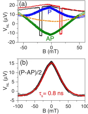
Therefore, modulating the excitation current around zero on a time scale shorter than it takes for the nuclear field to build up results inBN ≈0. As the time needed to build upBNis usually on the order of minutes [41,44], low-frequency ac excitation is sufficient to suppress DNP effects. In Fig. 3(a)we show ac measurements usingIrmsac =1μA at the frequency off = 13 Hz of the same sample presented before in Fig.2using a dc setup. The anomalies in the Hanle traces, visible in Fig.2(e), have disappeared and, after removing the background, the curve can be well fitted with Eq. (2), givingτs =0.8 ns, in contrast to the value of 1 ns extracted from dc measurements.
It is worth noting that also the NLSV signal looks closer to theoretical expectation, compared to the one shown in Fig.2.
VNLbase is close to zero for ac measurements, reflecting that VNLbaseis quite symmetric with respect toI =0 for low bias, as can be seen in Fig.2(d). Although the value ofVNLbase(B)
-50 0 50
-20 -10 0 10 20
P
V
NL( μ V)
B (mT)
AP (a)
-100 -50 0 50 100
-5 0 5 10 15
(P-AP)/2 (b)
V
NL( μ V)
B (mT) τ
s= 0.8 ns
FIG. 3. (a) ac measurement (Irmsac =1μA andf =13 Hz) of the NLSV signal (black and red lines) and the Hanle effect (blue and olive symbols) for parallel (P) and antiparallel (AP) contact configuration of the same contacts as in Fig.2. The dashed orange line shows the magnetoresistance of the background voltageVNLbase(Bz)=(VNLAP+ VNLP)/2. (b) Hanle fit to the data, after removing the background, yielding a spin lifetime of 800 ps.
gets reduced in ac measurements, it is still present [the orange line in Fig.3(a)] and distorts the Hanle curves. We discuss this field dependence in more detail in the next section.
To demonstrate that ac excitation indeed suppresses DNP effects in our samples we conduct a control experiment. For that, we perform Hanle measurements in the presence of a small in-plane magnetic field By= +2 mT. In this case the presence of a nuclear field is manifested by two satellite peaks appearing additionally to the main depolarization peak atBz= 0 [41]. This results from the interplay between the total external magnetic field Bextand the nuclear field BN. Due to the in- plane componentBy the total Bextis no longer normal to the plane of the 2DES. According to Eq. (3), the orientation ofBN
is controlled by the sign ofBext·Sandbn. Because in case of GaAsbn<0, BNis parallel (antiparallel) to Bextwhen Bext· S<(>)0. For antiparallel orientation the condition Bext=
−BNcan be adjusted. For this condition the total fieldBtot≈0, Hanle-type spin dephasing is suppressed, and the spin signal is partially restored, giving rise to the satellite peaks.
In Fig. 4 we present Hanle traces obtained for Irmsac = 700 nA, corresponding to alternating the injection current between approximately ±1μA. The measurements were performed on a sample withwy =2.5μm in order to reduce the influence of the background magnetoresistance, discussed in more details in Sec. III D. Figure 4(a) displays a wide Hanle curve without any satellite peaks which can be well fitted with the standard equation. The situation changes when an additional dc current of±5μAis applied to the injection
0.1 1 10 0
5 10 15 20 25
-50 0 50
-4 0 4 8 12 (a)
VNL (μV)
Bz (mT)
-50 0 50
0 4 8 12 16
(b) 20
VNL (μV)
Bz (mT)
-50 0 50
-10 -5 0 5 10
(c) 15
VNL (μV)
Bz (mT)
(d)
τs (ns)
IACRMS (µA) VNL
IAC
VNL IAC+IDC
IDC=+5 µA By=+2 mT
IDC=-5 µA By=+2 mT By=+2 mT
FIG. 4. (a) Low-amplitude (Irmsac =700 nA), low-frequency (f = 13 Hz) ac measurements with an in-plane componentBy = +2 mT.
(b) and (c) Measurements like in (a) but with an additional dc bias across the injector. Satellite peaks appear in (c) for Idc= −5μA.
Measurements were performed on a sample withwy =2.5μm with the injector-detector separation L=3.75μm. Insets illustrate the relative orientation of the external fieldBextand the nuclear fieldBN
in each case. Arrows mark the position of satellite peaks at Bext=
−BN (d) Spin-relaxation time extracted from ac measurements for different values of excitation current. Measurements were performed on a sample withwy=5μm and with the contacts aligned along [1¯10] direction.
contact, shown in Figs.4(b)and4(c). The applied dc current creates a spin accumulation of certain spin orientation which in turn results in a finite nuclear fieldBN. Thus, the Hanle curves get narrower for both current polarities and additional satellite peaks appear for negative currents, i.e., for Idc= −5μA, shown in Fig. 4(c). As the satellites appear for negative currents we can conclude that the injected spins are oriented along the applied in-plane component By = +2 mT (see the corresponding inset). Because the magnetization of the contactsMwas saturated before the Bzsweep atBy = −0.5 T, the spins injected forI <0 into the channel are, as expected, antiparallel toM.
The experiment described above suggests that low ac excitation indeed suppresses DNP so that an analysis of the Hanle trace delivers realistic spin parameters for our 2DES.
This, however, holds only for currents of 1μA and below.
For increasing current strength, the asymmetry of the nonlocal voltage between injection and extraction increases, so that the spin accumulation generated at positive and negative half waves of the injection current does not average to zero. Consequently DNP builds up. In Fig. 4(d) we show spin-relaxation times extracted from Hanle curves for different ac current amplitudes. Obviously, for Iac>1μA τs values are growing, indicating the increasing nuclear magnetic field which narrows the Hanle traces. For Iac<1μA τs stays essentially constant and reflects the true spin-relaxation time.
These results were obtained from measurements on the sample withwy =5μm, but similar behavior was observed also for
the other samples. The bottom line of this section is that for reliable extraction of spin parameters from Hanle traces in GaAs based 2DESs one needs to resort to low level ac measurements in order to suppress DNP.
D. Geometrical effects
A small background signalVNLbase(Bz) with weak depen- dence on B is another ingredient which eases analysis of Hanle traces. Below we show that the aspect ratio L/wy
strongly influences the background. It turns out that a large L/wy, i.e., an injector-detector separation L much larger than the channel widthwy, suppresses the background signal.
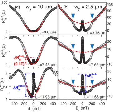
In Fig. 5 we show Hanle measurements from two samples having different channel widthswy, namely, 10 and 2.5μm, but nearly the same L’s (see figure). All graphs show the nonlocal resistanceRNL=VNL/I, with injector currentI, in the magnetic field range between±0.5 T. Both samples display between ±0.1 T and for all lengths L Hanle signals, with RNLs (Bz) superimposed on a B-field dependent background resistanceRNLbase(B)=VNLbase(B)/I.RNLbase(B) is, however, sub- stantially different for both samples. For the 10-μm-wide channel, the background can be well described by a parabolic dependence (red dashed line), as observed before for bulk devices [3,5]. Differently than for bulk samples, however, in case of 2DES samples RNLbase(B) clearly dominates the spin signal, particularly for smallL/wy.RNLbase(B) decreases with
0 30 60 90 120
L=3.75 µm
L=7.65 µm-10 0 10 20
L=11.65 µm -400 -200 0 200 400
-10 0 10 20
Bz (mT) ΔΔΔΔRHanlenl 0
250
Rdet1 nl(Ω)
L=3.6 µm
L=7.45 µm 0
25
ΔΔΔΔRbasenl (0.1T) Rdet2 nl(Ω)
L=11.95 µm -400 -200 0 200 400 1
2 3
Rdet3 nl(Ω)
Bz (mT) ΔΔΔΔRHanlenl
(a) wy= 10 µm (b) wy= 2.5 µm
FIG. 5. ac Hanle traces for different injector-detector separations L, measured on devices with a 10-μm-wide (a) and 2.5-μm-wide (b) channel. Red dashed lines are quadratic fits to the background magnetoresistance. Blue triangles indicate field values at which the spin signal is restored due to alignment of spins along Bz, after the magnetization of the the contacts has been rotated out of plane. The magnitude of the Hanle signalRHanleNL and the change of the nonlocal background resistanceRbaseNL forB=0.1 T are also indicated. The 10-μm-wide (2.5-μm-wide) sample has its contacts aligned along [100] ([1¯10]) crystallographic direction.
increasingL/wy, nevertheless it still affects the spin signal at low B.RbaseNL (B) of the narrow channel, shown in Fig.5(b), has the much weakerBdependence. Similarly as for the wide sample,RNLbase(B) decreases withL/wy. Because of the weak Bz dependence of RbaseNL in the 2.5-μm-wide sample, more features become resolved, (partially) masked by the larger background magnetoresistance in the wide channel. In the narrow sample Shubnikov-de Haas oscillations appear in the nonlocal resistance for all differentLat fieldsB >300 mT.
The oscillatory behavior of the nonlocal longitudinal resistance in 2DESs has been investigated before [50,51]. It has been explained in terms of the interplay between bulk channels and edge channels formed in the presence of a strong out-of-plane magnetic field. Secondly, a feature between 160 and 200 mT, marked by blue arrowheads, stands out, which is ascribed to the magnetization of (Ga,Mn)As being rotated out of plane. This orients the injected spins along the applied field, suppressing spin precession and restoring the spin signal. The restored spin signal is, however, lower than at Bz=0, probably due to the lower Pinj for out-of-plane oriented spins [5,52] and lower spin-relaxation times of out-of-plane spins in 2DESs [1].
The aspect ratio dependence ofRNLbase(B) resembles closely the geometry induced magnetoresistance observed in standard Hall devices [53]. It is commonly known that the magnetoresis- tance in such samples is described by the sum of physical mag- netoresistance and geometrical magnetoresistance [53,54].
The geometrical magnetoresistance is the strongest for very short and wide samples, with the Corbino disk as the limiting case, and is vanishing for infinitely long samples. Generally, the magnetoresistanceR(B) is given by
R(B)
R(0) = ρ(B)
ρ(0)Gr(B,L/w), (6)
with R(0) the resistance at B=0 and with ρ(B) andρ(0) the resistivities of devices withL/w→ ∞with and without appliedB field, respectively.Gr(B,L/w) is the geometrical factor, dependent on the Hall angle μB and L/w. Gr is equal to 1 forL/w→ ∞and is given by 1+(μB)2for the Corbino disk in the limitL/w→0.Grdetermines usually the B-field dependence of the total MR, particularly for degenerate systems, whenρ(B)=ρ(0). Depending on the aspect ratio, Gr shows a quadratic increase at low B, which is stronger for wide and short samples, and becomes linear inBin large magnetic fields [54]. To resolve the Hanle spin signal against the background magnetoresistance (BMR), the amplitude of the signal RNLHanle should be larger than the change of the background resistance RNLbase(B)=RNLbase(B)−RNLbase(0) in the field range required to fully dephase a spin. The typical field range for which this happens is B ∼0.1 T in our samples. In order to determine a suitable RNLbase(B) we fitted the measured RNLbase(B) with a parabolic function (red dashed lines in Fig. 5). We then take the background at 0.1 T, i.e., RbaseNL (B=0.1T) to quantify its influence on Hanle measurements. Corresponding data for both samples, discussed in Fig.5, are plotted in Fig.6(a)as a function ofL.
The background decreases for both samples with increasingL and is substantially smaller for the narrow channel. In the same figure we compareRbaseNL (B=0.1 T) with the amplitude of
(a)
(b)
0 5 10 15
0 5 10 15 20 25
ΔRbasenl 2.5 µm ΔRbasenl 10 µm
ΔR nl (B=0.1T)(Ω)
L (µm)
0 10 20 30 40 50
ΔRHanlenl 2.5 µm ΔRHanlenl 10 µm
ΔRHanle nl(Ω)
0 1 2 3 4 5 6 7 8
1 10 100 1000
2.5 µm 8.0 µm 2.5 µm 10 µm 4.0 µm 10 µm 5.0 µm 10 µm 6.0 µm 10 µm
ΔRHanle nl / ΔRbase nl
L/wy
FIG. 6. (a) Distance dependence of RNLbase(B) at B=0.1 T (black) and of nonlocal Hanle signal RHanleNL (red). Diamonds and circles represent the measurements for 2.5- and 10-μm-wide channels, respectively. Solid red lines are exponential fits ofRNLHanle, with the correspondingλsf ≈12 and 6μm forwy=2.5 and 10μm, respectively. Black lines are guides to the eye. (b) Signal-to- background ratios obtained from measurements on ten different samples plotted vs aspect rationL/wy. Red circles and diamonds correspond to data shown in (a); other symbols correspond to samples with variouswy, as indicated in the legend. Open (full) symbols correspond to channels along the [110] ([010]) crystallographic direction. Estimated error bars are smaller than the size of the symbols. The line is a guide to the eye.
the Hanle peak,RHanleNL . For both samples the background signal decays much faster withLthan the Hanle signal. In case of the 2.5-μm-wide (10-μm-wide) sampleRHanleNL measured at the second and the third detector correspond, respectively, to about 80 and 50% (60 and 20%) of the Hanle signal at the first detector. On the same length scales the nonlocal background, however, drops to 15 and 10% (20 and 2%) of the RNLbase at the first detector. Since the Hanle signal scales with 1/wy
[see Eqs. (1) and (2)], the ratioRNLHanle/RNLbase(0.1 T) is much larger for the narrow channels. This is shown in Fig.6(b)where we compare data from ten different samples having various channel widths. Although the ratio varies a bit from sample to sample, it is obvious that the signal-to-background ratio increases significantly with increasing L/wy ratio, reaching
values of 100. Long and narrow samples are therefore preferable for Hanle measurements in 2DESs.
Finally, we compare our results on 2D systems with those reported for bulk semiconductors so far [3,5]. Parabolic BMR has been commonly observed in those measurements, being fully consistent with our discussion on geometrical magnetoresistance, which is expected to to be proportional to (μB)2 at small Hall angles, given by μB. This condition is satisfied for a wide range of magnetic fields for typical bulk mobilities. Also the fact that the magnitude of the BMR observed in our experiments on bulk devices [5] is typically three orders of magnitude lower than in the 2DES samples can be directly linked to the much higher mobilities of 2DESs. We conclude, therefore, that in the case of high mobility 2DES channels a proper choice of the sample geometry is more crucial for successful electrical measurements of Hanle spin precession than in the case of low mobility bulk systems.
E. Spin lifetimes in the 2DES
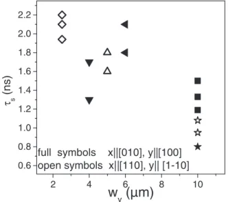
The low excitation ac technique discussed above allows us to perform reliable measurements of spin-relaxation timesτsin 2D systems, particularly if the background magnetoresistance is sufficiently suppressed. In Fig. 7 we show results from seven samples having ferromagnetic contacts aligned either in [010] or in [110] direction and having different channel widthswy. All extractedτs values are in the range between 0.8 and 2.5 ns and thus significantly larger than expected for pure Dyakonov-Perel spin relaxation in 2DESs [1].τs values of order 1 ns are, however, consistent with recent results obtained from Kerr effect measurements [19]. As discussed there, spin relaxation in zinc-blende-based 2D systems can be highly anisotropic with a high relaxation rate for spins oriented along [1¯10] and a low rate for [110] [55,56]. For the latter orientation, values of up to 8 ns have been calculated [57].
2 4 6 8 10
0.6 0.8 1.0 1.2 1.4 1.6 1.8 2.0 2.2
τ s (ns)
w
y(µm)
full symbols x||[010], y||[100]
open symbols x||[110], y|| [1-10]
FIG. 7. Spin-relaxation times obtained from ac Hanle measure- ments (Irmsac =700 nA) for seven different samples with various widthswy and different crystallographic orientation of the channel and of the ferromagnetic contacts. Same symbols correspond to different detector contacts of the same device. For any given sample, we use also the same symbols as in Fig.6(b).
In Hanle experiments, however, an external magnetic field is applied in z direction causing spin precession in the (001) plane. As a consequence the extracted spin lifetimes are given by the geometrical mean of spin lifetimes along [1¯10] and [110] directions [58]. The fact that we do not observe a clear dependence of the spin lifetime on the crystallographic direction in Fig.7 is consistent with our expectation that in experiment a mean value ofτsis being measured. We observe, however, a small dependence ofτson the width of the channel, with largerτs values measured for narrower channels. This is expected theoretically [59,60] and has been observed in experiments before [38,61]. It should be noted, though, that our results are rather preliminary, and they have been mostly obtained from devices with not optimalL/wy. One should also keep in mind that the properties of the 2D system can differ from sample to sample as they depend, among other things, on the illumination conditions. A systemic investigation of the dependence of τs on geometry in 2DESs requires thus more experiments. Measurements on samples with channels narrower than 1μm would be particularly interesting, as one expects that then the lateral confinement affects spin relaxation much more [38,61].
With the extracted spin lifetimes of order 1 ns and measured spin-diffusion lengths λsf of the order of a few microns we can calculate the spin-diffusion constants,Ds =λ2sf/τs. For the sample shown in Fig. 3, e.g., the measured τs = 0.8 ns and λsf =2.3μm giveDs=6.5×10⁻³ m2/s. From magnetotransport experiments we obtain a different value, De=0.22 m2/s. Thus, the spin-diffusion constantDs in our device is much smaller than the charge diffusion constant De. This is in line with previous results [9,12,38,40], where this effect was ascribed to the importance of electron-electron interactions in 2D systems [39].
IV. CONCLUSION
We have investigated how dynamical nuclear polarization and background magnetoresistance affect the analysis of spin relaxation in nonlocal spin injection/detection experiments in high mobility two-dimensional electron systems. The DNP effect, which causes too long spin-relaxation timesτs being extracted from Hanle measurements due to the buildup of a nuclear field, can be suppressed by low-frequency and low bias ac measurements. Measurements carried out under these conditions giveτs values between 0.8 and 2.5 ns. We have further shown that the background magnetoresistance which can obscure Hanle signals can be effectively reduced by reducing the channel widthwy and increasing the injector- detector separationL. Combining low bias ac measurement with a large aspect ratio, L/wy 1, allows the reliable extraction ofτs and related parameters, like spin-relaxation lengthλsand spin-diffusion constantDs, from nonlocal spin injection/detection experiments in 2DESs.
ACKNOWLEDGMENT
This work was supported by the German Science Founda- tion (Deutsche Forschungsgemeinschaft) via Grant No. SFB 689.
[1] I. Žuti´c, J. Fabian, and S. Das Sarma,Rev. Mod. Phys.76,323 (2004).
[2] S. Datta and B. Das,Appl. Phys. Lett.56,665(1990).
[3] X. Lou, C. Adelmann, S. A. Crooker, E. S. Garlid, J. Zhang, K. S. M. Reddy, S. D. Flexner, C. J. Palmström, and P. A.
Crowell,Nat. Phys.3,197(2007).
[4] I. Appelbaum, B. Huang, and D. J. Monsma,Nature (London) 447,295(2007).
[5] M. Ciorga, A. Einwanger, U. Wurstbauer, D. Schuh, W.
Wegscheider, and D. Weiss,Phys. Rev. B79,165321(2009).
[6] S. P. Dash, S. Sharma, R. S. Patel, M. P. de Jong, and R. Jansen, Nature (London)462,491(2009).
[7] R. Jansen,Nat. Mat.11,400(2012).
[8] P. Bruski, Y. Manzke, R. Farshchi, O. Brandt, J. Herfort, and M.
Ramsteiner,Appl. Phys. Lett.103,052406(2013).
[9] M. Ciorga,J. Phys.: Condens. Matter28,453003(2016).
[10] H. C. Koo, J. H. Kwon, J. Eom, J. Chang, S. H. Han, and M. Johnson,Science (NY)325,1515(2009).
[11] M. Oltscher, M. Ciorga, M. Utz, D. Schuh, D. Bougeard, and D. Weiss,Phys. Rev. Lett.113,236602(2014).
[12] C. P. Weber, N. Gedik, J. E. Moore, J. Orenstein, J. Stephens, and D. D. Awschalom,Nature (London)437,1330(2005).
[13] D. Stich, J. Zhou, T. Korn, R. Schulz, D. Schuh, W. Wegscheider, M. W. Wu, and C. Schüller, Phys. Rev. Lett. 98, 176401 (2007).
[14] T. Korn,Phys. Rep.494,415(2010).
[15] W. Hanle,Z. Phys.30,93(1924).
[16] A. N. M. Zainuddin, S. Hong, L. Siddiqui, S. Srinivasan, and S.
Datta,Phys. Rev. B84,165306(2011).
[17] M. I. D’yakonov and V. Perel’, Sov. Phys. JETP33, 1053 (1971) [Zh. Eksp. Teor. Fiz.60, 1954 (1971)].
[18] M. I. D’yakonov and V. Perel’, Sov. Phys. Solid State13, 3023 (1972) [Fiz. Tverd. Tela13, 3581 (1971)].
[19] M. Buchner, T. Kuczmik, M. Oltscher, M. Ciorga, T. Korn, J.
Loher, D. Schuh, C. Schüller, D. Bougeard, D. Weiss, and C. H.
Back,Phys. Rev. B95,035304(2017).
[20] M. Kohda, Y. Ohno, K. Takamura, F. Matsukura, and H. Ohno, Jpn. J. Appl. Phys.40,L1274(2001).
[21] E. Johnston-Halperin, D. Lofgreen, R. K. Kawakami, D. K.
Young, L. Coldren, A. C. Gossard, and D. D. Awschalom, Phys. Rev. B65,041306(2002).
[22] P. V. Dorpe, Z. Liu, W. V. Roy, V. F. Motsnyi, M. Sawicki, G. Borghs, and J. D. Boeck, Appl. Phys. Lett. 84, 3495 (2004).
[23] M. Ciorga, M. Utz, D. Schuh, D. Bougeard, and D. Weiss, Phys. Rev. B88,155308(2013).
[24] H. Störmer, R. Dingle, A. Gossard, W. Wiegmann, and M.
Sturge,Solid State Commun.29,705(1979).
[25] M. Johnson and R. H. Silsbee, Phys. Rev. Lett. 55, 1790 (1985).
[26] J. Fabian, A. Matos-Abiague, C. Ertler, P. Stano, and I. Žuti´c, Acta Phys. Slov.57, 565 (2007).
[27] J. Fabian and I. Žuti´c, inSpintronics: From GMR to Quantum Information, edited by S. Blügel, D. Bürgler, M. Morgenstern, C. Schneider, and R. Waser (Forschungszentrum Jülich, Jülich, Germany, 2009),arXiv:0903.2500.
[28] F. J. Jedema, A. T. Filip, and B. J. van Wees,Nature (London) 410,345(2001).
[29] S. Garzon, I. Žuti´c, and R. A. Webb,Phys. Rev. Lett.94,176601 (2005).
[30] Y. Ji, A. Hoffmann, J. E. Pearson, and S. D. Bader,Appl. Phys.
Lett.88,052509(2006).
[31] Y. Otani and T. Kimura, Phil. Trans. R. Soc. A369, 3136 (2011).
[32] T. Sasaki, T. Oikawa, M. Shiraishi, Y. Suzuki, and K. Noguchi, Appl. Phys. Lett.98,012508(2011).
[33] M. Johnson and R. H. Silsbee,Phys. Rev. B76,153107(2007).
[34] F. L. Bakker, A. Slachter, J.-P. Adam, and B. J. van Wees, Phys. Rev. Lett.105,136601(2010).
[35] S. Kasai, S. Hirayama, Y. K. Takahashi, S. Mitani, K. Hono, H.
Adachi, J. Ieda, and S. Maekawa,Appl. Phys. Lett.104,162410 (2014).
[36] F. J. Jedema, H. B. Heersche, A. T. Filip, J. J. A. Baselmans, and B. J. van Wees,Nature (London)416,713(2002).
[37] V. F. Motsnyi, J. De Boeck, J. Das, W. Van Roy, G. Borghs, E. Goovaerts, and V. I. Safarov, Appl. Phys. Lett. 81, 265 (2002).
[38] P. Altmann, M. Kohda, C. Reichl, W. Wegscheider, and G. Salis, Phys. Rev. B92,235304(2015).
[39] I. D’Amico and G. Vignale,Europhys. Lett.55,566(2001).
[40] L. Yang, J. D. Koralek, J. Orenstein, D. R. Tibbetts, J. L. Reno, and M. P. Lilly,Nat. Phys.8,153(2011).
[41] G. Salis, A. Fuhrer, and S. F. Alvarado,Phys. Rev. B80,115332 (2009).
[42] M. K. Chan, Q. O. Hu, J. Zhang, T. Kondo, C. J. Palmstrøm, and P. A. Crowell,Phys. Rev. B80,161206(2009).
[43] C. Awo-Affouda, O. M. J. van ’t Erve, G. Kioseoglou, A. T.
Hanbicki, M. Holub, C. H. Li, and B. T. Jonker,Appl. Phys.
Lett.94,102511(2009).
[44] J. Shiogai, M. Ciorga, M. Utz, D. Schuh, T. Arakawa, M. Kohda, K. Kobayashi, T. Ono, W. Wegscheider, D. Weiss, and J. Nitta, Appl. Phys. Lett.101,212402(2012).
[45] P. Van Dorpe, W. Van Roy, J. De Boeck, G. Borghs, P. Sankowski, P. Kacman, J. A. Majewski, and T. Dietl, Phys. Rev. B72,205322(2005).
[46] Y. Ohno, R. Terauchi, T. Adachi, F. Matsukura, and H. Ohno, Phys. Rev. Lett.83,4196(1999).
[47] P. Van Dorpe, W. Van Roy, J. De Boeck, and G. Borghs, Phys. Rev. B72,035315(2005).
[48] D. Paget, G. Lampel, B. Sapoval, and V. I. Safarov,Phys. Rev.
B15,5780(1977).
[49] A. Fuhrer, S. F. Alvarado, G. Salis, and R. Allenspach, Appl. Phys. Lett.98,202104(2011).
[50] P. L. McEuen, A. Szafer, C. A. Richter, B. W. Alphenaar, J. K.
Jain, A. D. Stone, R. G. Wheeler, and R. N. Sacks,Phys. Rev.
Lett.64,2062(1990).
[51] K. Tsukagoshi, K. Oto, S. Takaoka, K. Murase, Y. Takagaki, K. Gamo, and S. Namba, Solid State Commun. 80, 797 (1991).
[52] A. Einwanger, M. Ciorga, U. Wurstbauer, D. Schuh, W.
Wegscheider, and D. Weiss, Appl. Phys. Lett. 95, 152101 (2009).
[53] R. S. Popovi´c, Hall Effect Devices: Magnetic Sensors and Characterization of Semiconductors (Adam Hilger, Bristol, 1991).
[54] H. J. Lippmann and F. Kuhrt, Z. Naturforsch.13a, 462 (1958).
[55] N. S. Averkiev and L. E. Golub, Phys. Rev. B 60, 15582 (1999).
[56] N. S. Averkiev, L. E. Golub, and M. Willander, J. Phys.:
Condens. Matter14,R271(2002).
[57] D. Stich, J. Zhou, T. Korn, R. Schulz, D. Schuh, W. Wegscheider, M. W. Wu, and C. Schüller,Phys. Rev. B76,205301(2007).
[58] R. Völkl, M. Schwemmer, M. Griesbeck, S. A. Tarasenko, D.
Schuh, W. Wegscheider, C. Schüller, and T. Korn,Phys. Rev. B 89,075424(2014).
[59] A. A. Kiselev and K. W. Kim, Phys. Rev. B 61, 13115 (2000).
[60] S. Kettemann,Phys. Rev. Lett.98,176808(2007).
[61] A. W. Holleitner, V. Sih, R. C. Myers, A. C. Gossard, and D. D.
Awschalom,Phys. Rev. Lett.97,036805(2006).